EP0201635B1 - Telecommunication line circuit - Google Patents
Telecommunication line circuit Download PDFInfo
- Publication number
- EP0201635B1 EP0201635B1 EP85200774A EP85200774A EP0201635B1 EP 0201635 B1 EP0201635 B1 EP 0201635B1 EP 85200774 A EP85200774 A EP 85200774A EP 85200774 A EP85200774 A EP 85200774A EP 0201635 B1 EP0201635 B1 EP 0201635B1
- Authority
- EP
- European Patent Office
- Prior art keywords
- coupled
- output
- terminals
- operational
- circuit
- Prior art date
- Legal status (The legal status is an assumption and is not a legal conclusion. Google has not performed a legal analysis and makes no representation as to the accuracy of the status listed.)
- Expired
Links
- 101100455096 Saccharomyces cerevisiae (strain ATCC 204508 / S288c) LOA1 gene Proteins 0.000 claims description 25
- 230000015572 biosynthetic process Effects 0.000 claims description 10
- 238000003786 synthesis reaction Methods 0.000 claims description 10
- 238000001514 detection method Methods 0.000 claims description 5
- 230000002457 bidirectional effect Effects 0.000 abstract description 4
- 239000004020 conductor Substances 0.000 description 6
- 101150115013 DSP1 gene Proteins 0.000 description 3
- 101150052726 DSP2 gene Proteins 0.000 description 3
- 101100067427 Saccharomyces cerevisiae (strain ATCC 204508 / S288c) FUS3 gene Proteins 0.000 description 3
- 101100015484 Saccharomyces cerevisiae (strain ATCC 204508 / S288c) GPA1 gene Proteins 0.000 description 3
- 230000000694 effects Effects 0.000 description 3
- 230000005540 biological transmission Effects 0.000 description 2
- 230000001105 regulatory effect Effects 0.000 description 2
- 230000002194 synthesizing effect Effects 0.000 description 2
- 101100534112 Sus scrofa SPMI gene Proteins 0.000 description 1
- 230000003321 amplification Effects 0.000 description 1
- 230000000903 blocking effect Effects 0.000 description 1
- 239000003990 capacitor Substances 0.000 description 1
- 238000006243 chemical reaction Methods 0.000 description 1
- 230000001419 dependent effect Effects 0.000 description 1
- 230000009977 dual effect Effects 0.000 description 1
- 238000001914 filtration Methods 0.000 description 1
- 238000000034 method Methods 0.000 description 1
- 238000003199 nucleic acid amplification method Methods 0.000 description 1
- 238000009738 saturating Methods 0.000 description 1
Images


Classifications
-
- H—ELECTRICITY
- H04—ELECTRIC COMMUNICATION TECHNIQUE
- H04M—TELEPHONIC COMMUNICATION
- H04M19/00—Current supply arrangements for telephone systems
- H04M19/02—Current supply arrangements for telephone systems providing ringing current or supervisory tones, e.g. dialling tone or busy tone
- H04M19/026—Arrangements for interrupting the ringing current
-
- H—ELECTRICITY
- H04—ELECTRIC COMMUNICATION TECHNIQUE
- H04M—TELEPHONIC COMMUNICATION
- H04M19/00—Current supply arrangements for telephone systems
- H04M19/001—Current supply source at the exchanger providing current to substations
- H04M19/005—Feeding arrangements without the use of line transformers
-
- H—ELECTRICITY
- H04—ELECTRIC COMMUNICATION TECHNIQUE
- H04M—TELEPHONIC COMMUNICATION
- H04M19/00—Current supply arrangements for telephone systems
- H04M19/02—Current supply arrangements for telephone systems providing ringing current or supervisory tones, e.g. dialling tone or busy tone
-
- H—ELECTRICITY
- H04—ELECTRIC COMMUNICATION TECHNIQUE
- H04M—TELEPHONIC COMMUNICATION
- H04M3/00—Automatic or semi-automatic exchanges
- H04M3/005—Interface circuits for subscriber lines
-
- H—ELECTRICITY
- H04—ELECTRIC COMMUNICATION TECHNIQUE
- H04M—TELEPHONIC COMMUNICATION
- H04M3/00—Automatic or semi-automatic exchanges
- H04M3/22—Arrangements for supervision, monitoring or testing
- H04M3/2272—Subscriber line supervision circuits, e.g. call detection circuits
Definitions
- the present invention relates to a telecommunication line circuit including a pair of operational line amplifiers coupled to first terminals of a pair of line feed resistances whose second terminals are coupled to a two-wire bi-directional line, said first and second pairs of terminals being coupled to a sensing circuit which is able to sense the DC/AC current in said feed resistances and which together with said operational amplifiers is included in AC/DC feedback circuits enabling to synthesize desired characteristics and values of AC impedance and DC resistances from said AC/DC current feed resistances, and said first pair of terminals being moreover coupled to a generator of a ringing signal.
- Such a telecommunication line circuit is already known from Belgian patent No 898049. Therein the sensing circuit is not adapted to sense a ringing signal and to do so a separate sensing circuit would be required .
- An object of the present invention is to provide a telecommunication line circuit of the above type, but wherein the sensing circuit is also able to sense said ringing signal.
- said sensing circuit includes a Herter bridge of which also said pair of line feed resistances form part and which has an output coupled to respective inputs of an operational sense amplifier, that said inputs of said operational sense amplifier are coupled to a first bias source through respective first bias resistances and that the non-inverting input of said operational sense amplifier is connected to a second bias source through a second bias resistance whilst its output is connected to its inverting input through a feedback third resistance, all in such a manner that the AC/DC differential signal at the output of the Herter bridge is converted to an AC/DC single-ended signal at the output of the operational amplifier proportional to the sum of the signal drops across said feed resistances.
- the AC/DC differential signal supplied to the sence amplifier is devoid of longitudinal current and by a suitable selection of the Herter bridge resistances and of the resistances diretly associated to the operational amplifier the output signal of this amplifier not only is indicative of the presence of the ringing signal but also suitable for being used for synthesizing AC and DC impedances.
- the telecommunication circuit shown in Fig. 1 includes a line circuit LC which is connected in cascade with a switch circuit HVC between a telecommunication line with conductors LI0 and LI1, connected to a subset TSS, and a switching network SNW.
- Line circuit LC includes the cascade connection of a SLIC, a Digital Signal Processor DSP, a TransCoder and Filter circuit TCF and a Dual Processor Terminal Controller DPTC.
- Subset TSS includes a normally open hook switch HS connected between the line conductors LI0 and LI1.
- Switch circuit HVC is for instance of the type disclosed in Belgian patent 897 772. It includes 4 pairs of bidirectional switches sw00, sw01 to sw30, sw31 as shown and has line terminals L0 and L1 connected to line conductors LI0 and LI1 respectively, test terminals T0 and T1 connected to a test circuit TC, ringing terminals RG0 and RG1 connected to a ringing circuit RC, tip and ring terminals TP and RG connected to the like named outputs of line amplifiers LOA0 and LOA1 in the SLIC respectively and terminals STA, STB, SRA, SRB connected to like named terminals of a sensing circuit SENC in the SLIC.
- the line terminals L0/L1 are connected to TP/RG via the series connection of sw00/01, 50 ohms line feed resistors R0/1 and sw10/11 respectively.
- the respective junction points STB and SRA of sw00 and R0 and of sw01 arid R1 are connected to TC via sw20 and sw21 respectively, whilst the respective junction points STA and SRB of R0 and sw10 and of R1 and sw11 are connected to RC via sw30 and sw31 respectively.
- series switches sw00, sw01, sw10 and sw11 are closed, whereas the other shunt switches are open.
- switches are controlled by the SLIC so that HVC is able to establish either one of the following connections : between TSS and SLIC (LOA0, LOA1 and SENC);TC and TSS : SLIC (LOA0, LOA1) and TC; RC and TSS; RC and SLIC (SENC).
- the function of TC is to test the connection to TSS and to the SLIC and that of RC is to apply a ringing signal to this line and to SENC in the SLIC.
- RC is able to connect ground through sw30 and the negative battery BA of -48 or -60 Volts in series with a ringing source RS of 90 Volts RMS through sw31.
- the Subscriber Line Interface Circuit SLIC is a two-wire bidirectional circuit on the side of TSS and a four-wire one towards SNW. It has a speech receive input terminal Rx (with ground return) and a speech transmit output Tx (again with ground return), Rx and Tx being connected to DSP.
- the SLIC further has a 12 kHz or 16 kHz metering signal input terminal MTCF connected to TCF, data input and output terminals DSP1 and DSP2 connected to DSP and the above mentioned terminals STA, STB, SRA, SRB, TP and RG connected to HVC.
- the digital signal processor DSP converts a digital speech signal received from TCF into an analog speech signal which is then applied to the speech receive terminal Rx of the SLIC. Conversely it converts an analog speech signal received via the speech transmit terminal Tx of the SLIC into a digital version which is applied to TCF.
- DSP also includes an echo canceller circuit.
- a plurality of drive bits are transmitted by DSP to data terminal DSP1 of the SLIC, as described in the above mentioned Belgian patent 898 049.
- One of these drive bits is a ringing bit RNG indicating that ringing is to be performed (1) or not (0).
- the DSP also receives on its data terminal DSP2 a plurality of control data bits transmitted by the SLIC. Two of these bits are :
- the TCF performs a transcoding operation on digital signals received from the DSP and the DPTC and is also adapted to supply a metering signal MTCF to the SLIC. These operations are described in the Belgian patents 897 771 and 897 773.
- the DPTC performs the general control of the SLIC. Details of this circuit are described in the Belgian patents 898 959 and 898 960.
- circuit TCF and DSP are provided in common for a number of such lines, e.g. 8 lines, as indicated by the multipling arrows.
- Fig. 2 representing the SLIC of Fig. 1 in more detail.
- This circuit operates with the following voltages:
- the tip and ring outputs TP and RG of the line amplifiers LOA0 and LOA1 are connected to the respective feed resistances R0 and R1.
- These, together with the potentiometers comprising the resistances R2, R3 and and R4, R5 constitute the Herter bridge already discussed and having output terminals A and B connected to the inverting and non-inverting inputs of a sensing means constituted by operational amplifier OA2.
- the latter inputs are also connected to VAUX via respective bias resistances R6 and R7.
- the inverting input of OA2 is further connected to its output through feedback resistance R8, whilst its non-inverting input is further connected to VAG via bias resistance R9.
- the output CO1 of operational amplifier OA2 is connected to the inputs VEET of both LOA0 and LOA1, which have respective feedback resistances R10 and R11, through a DC feedback circuit DCFC which together with the amplifiers LOA0 and LOA1, the feed resistances R0 and R1 and the sensing circuit SENC constitutes a resistance synthesis circuit similar to the one disclosed in Belgian patent Nr. 898 049, i.e. a circuit to convert the value of each of the feed resistances R0 and R1 into a wanted resistance value.
- the output CO1 of the sensing circuit SENC is also connected via a DC blocking capacitor C1 in series with an amplifier stage DA3 including an operational amplifier, on the one hand to the inverting input TAC of LOA0 via resistance R12 and, on the other hand, to the non-inverting input RDC of LOA1 through resistance R13.
- the amplifiers LOA0 and LOA1, the resistances R0 and R1, the sensing circuit SENC, the amplifier stage OA3 and the resistances R12 and R13 constitute an AC impedance synthesis circuit able to convert the resistance value of R0 and R1 into a wanted AC impedance.
- this At impedance loop has certain simularities with the one disclosed in the above mentioned Belgian patents 898 052 and 898 049, but essentially differs therefrom in that it includes a Herter bridge and that the feedback control of LOA0 and LOA1 is a voltage control and not a current control.
- the inputs TDC of LOA0 and RDC of LOA1 are also connected through resistances R14 and R15 to the respective outputs VTI (BR2) and VRI (BRI) of a polarity reversal circuit PRC of the type disclosed in the above mentioned Belgian patent application 2/60362 which is a patent of addition to Belgian patent 898 051.
- the circuit PRC is able to apply a DC supply voltage V+ minus x to VTI (BR2) and a DC voltage VEET plus x to VRI (BR1) (BR1) or vice-versa, x being a voltage which comprises a fixed part and a variable part which is function of the amplitude of the metering signal applied to input terminal MTCF of the SLIC.
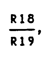
- the inputs TDC of LOA0 and RAC of LOA1 are connected to the output SMI of an operational amplifier OA4 via respective resistances R16 and R17.
- This amplifier has a negative feedback resistance R18 and a grounded non-inverting input.
- the above mentioned outputs MTCF of TCF and Rx of DSP are connected to the inverting input of OA4 in a way similar to the one disclosed in the above mentioned Belgian patent 898 049.
- MTCF is connected to OA4 via a decoupling and attenuator circuit DAC1, a gating circuit GC and a resistance R19 in series, and Rx is connected to OA4 via a decoupling and attenuator circuit DAC2.
- gating circuit GC is controlled by a bit SPMI indicating that a metering signal appearing on MTCF has to be entered in the SLIC or not.
- the output of the amplifier stage OA3 is also connected to the transmit output Tx, VAG via a decoupling and attenuator circuit DAC3 similar to DAC1 and DAC2. Because these circuits are similar, only DAC3 is shown in detail. It comprises, considered from the input to the output, a series capacitance C2 followed by a voltage divider constituted by the series resistance R21 and the shunt resistance R22 one end of which is connected to VAG whilst the junction of the resistances is connected to the live transmit terminal Tx.
- the output CO1 of OA2 is also connected to a comparator CO, on the one hand via the series connection of a filter circuit FC to eliminate metering signals from the input signal applied to it, an isolating unity gain amplifier OA6 and a passing gate PG1, unblocked by RNG i.e. the inverse of the ringing bit RNG, and, on the other hand, through the series connection of a filter circuit for filtering a ringing signal and preventing the comparator CO to react to spikes, and a passing gate PG2 unblocked by the ringing bit RNG.
- the last filter comprises a series resistance R23 and a shunt capacitance C3.
- R23 and C3 are interconnected through a passing gate PG3 unblocked by RNG, whilst C3 is shunted by passing gate PG4 unblocked by RNG .
- the branch FC, OA6 and PG1 in cooperation with CO serves to detect the closure of switch HS in TSS when there is no ringing and then provide a switch hook signal SHD on the like named output SHD of CO.
- the other branch R23, PG3, C3, PG4, PG2 in cooperation with CO serves to detect the closure of HS in TSS during a ringing operation and then generate a ring trip signal RT at the like named output RT of CO.
- Values of some of the above resistances and capacitances can be as follows : R0, R1 50 ohms; R2 to R5 60 kilo-ohms; R6, R7 10 kilo-ohms; R8, R9, R12, R13, R16, R17, R19 30 kilo-ohms; R10, R11, R14, R15 150 kilo-ohms; R18, R20 50 kilo-ohms; R23 170 kilo-ohms; C1, C3 470 nano-Farads.
- the capacitances C2 and the resistances R21 and R22 have values which are dependent on the use of the telecommunication circuit, e.g. national requirements.
- the sensing circuit SENC comprising the Herter bridge R0-R5 and the associated detection device constituted by the operational amplifier OA2 as well as and the resistances R6 - R9 will be considered.
- This amplifier has an input stage operating between V- and V+ and an output stage operating around VAG and between V- and VAUX. With the above given values this means that the input stage of OA2 operates between -48 Volts and 0 Volts, whereas its output stage functions between -7.5 Volts and 7.5 Volts with respect to VAG (-40.5 Volts).
- V5 - VAG (V2 - V1 + V4 - V3) .
- R8 R2 (5')
- the output voltage of OA2 given by (5') is directly proportional to the sum of the potential drops across R0 and R1.
- the ringing circuit RC shown in Fig. 1 is able to apply a ground to switch sw30 and a 90 Volts RMS ringing voltage superimposed on a -48 Volts DC voltage to switch sw31.
- V5 - VAG R0.I (7)
- the DC portion of this current flows exclusively through the bridge resistances R2 to R5, whereas the AC portion mainly flows through TSS because the latter offers an AC impedance which is much smaller than that offered by the resistances R2 to R5 having the high values given above.
- the ratio R8/R2 has been chosen equal to 1/2, so that V5 - VAG varies between +6 Volts and -6 Volts as a maximum and that there is no danger of saturating this output stage.
- the voltage V' may be outside the operating range 0, -48 Volts of the input stage of the operational amplifier OA2.
- the purpose of the connections of the inputs of OA2 to VAUX via the respective resistances R6 and R7 is to bring the common mode voltage V given by the above equation (6') and (10) within this operating range. This is realised because as soon as the above voltage V' is different VAUX a current starts flowing from or to VAUX via the resistances R6 and R7 so as to establish a common mode voltage V having a value comprised between V' and VAUX. This also follows from the comparison of the above relations (6') and (11) or (10) and (12) because V is smaller or larger than V' depending on V' being smaller or larger than VAUX.
- resistance R6 is chosen smaller than that of resistance R8 in order that more current should be derived to VAUX than to VAG from a predetermined value of V onwards. This value is equal to This is done in order that VAG which is a reference voltage for all the circuits SLIC, DSP, TCF and DPTC should be as little influenced as possible.
- the sensing circuit SENC use has been made of a Herter bridge so that an output voltage V5 - VAG is produced which is independent from common mode or longitudinal signals. But additionally the gain factor R2/R8 of the sensing circuit SENC has been chosen so as to prevent saturation of the output stage of OA2, and the connections of the inputs of OA2 to VAUX have been provided to reduce the common mode voltage V applied to these inputs,thereby preventing saturation of the input stage of OA2.
- RC applies the above mentioned AC/DC ringing signal to the terminals STA and SRB of the sensing circuit SENC.
- No DC current can flow to the subset TSS because the switch hook contact HS is still open, but the AC ringing signal operates the ringer in this subset and thus informs the subscriber that he is being called.
- This filter circuit is essentially provided to prevent spikes from operating the comparator CO and to reduce the amplitude of the ringing signal applied to it.
- speech or other signals may then be exchanged between the called TSS shown and a calling TSS coupled to the receive and transmit terminals Rx and Tx via SNW, DPTC, TCF and DSP.
- a speech signal from the TSS shown flows through resistances R0 and R1, sensing circuit SENC, capacitance C1, amplifier stage OA3 and network DAC3 to the transmit terminal Tx.
- Speech signals or other from the distant TSS are received on the receive terminal Rx and are applied to the output terminal SMI of OA4 via DAC2, OA5 and R20 in series. In OA4 this signal is amplified by a factor equal to or 1 with the above given values.
- this unbalanced signal is applied in push-pull with opposite phases to the line amplifiers LOA0 and LOA1 since it is simultaneously coupled to the non-inverting and inverting inputs TDC and RAC of these amplifiers.
- This signal is amplified by the factor in LOA0 and in LOA1 before being applied in a balanced way between the line conductors LI0 and LI1.
- a metering signal possibly applied to the input terminal MTCF of the SLIC is applied to the output SMI of OA4 via gating circuit GC,which has previously be unblocked,and OA4 and from there to the line via the amplifiers LOAD and LOA1 in the same way as described for the speech signal.
- the metering signal is amplified by a factor equal to or 5 3 with the above given values of R18 and R19.
- the output voltage V5 of the sensing circuit SENC is also used in an AC impedance synthesis circuit. Indeed, after DC has been removed from this output voltage by the capacitance C1 the resultant AC signal is applied via the amplifier stage OA3 to the line amplifiers LOA0 and LOA1.
- Amplifier stage OA3 may consist in an operational amplifier part of an overall SLIC integrated circuit design but with external components to determine the wanted complex impedance, e.g. a series input resistance and a feedback impedance comprising a resistance in series with another resistance shunted by a capacitance.
- the Herter bridge R0 - R5 is arranged at the junction of the unidirectional transmission and receive paths Tx and Rx and the bidirectional line LI0, LI1 and that it is used for the transmission of speech signals as well as of ringing signals although the latter have a much higher amplitude than the former. It is used,in combination with the comparator CO,for the detection of the closure of a hook switch contact during ringing or other instants. Finally, it is also used both in a resistance and in an impedance synthesis circuit.
Landscapes
- Engineering & Computer Science (AREA)
- Signal Processing (AREA)
- Power Engineering (AREA)
- Interface Circuits In Exchanges (AREA)
- Devices For Supply Of Signal Current (AREA)
- Burglar Alarm Systems (AREA)
- Details Of Aerials (AREA)
- Use Of Switch Circuits For Exchanges And Methods Of Control Of Multiplex Exchanges (AREA)
- Cable Transmission Systems, Equalization Of Radio And Reduction Of Echo (AREA)
- Input Circuits Of Receivers And Coupling Of Receivers And Audio Equipment (AREA)
- Emergency Protection Circuit Devices (AREA)
Abstract
Description
- The present invention relates to a telecommunication line circuit including a pair of operational line amplifiers coupled to first terminals of a pair of line feed resistances whose second terminals are coupled to a two-wire bi-directional line, said first and second pairs of terminals being coupled to a sensing circuit which is able to sense the DC/AC current in said feed resistances and which together with said operational amplifiers is included in AC/DC feedback circuits enabling to synthesize desired characteristics and values of AC impedance and DC resistances from said AC/DC current feed resistances, and said first pair of terminals being moreover coupled to a generator of a ringing signal.
- Such a telecommunication line circuit is already known from Belgian patent No 898049. Therein the sensing circuit is not adapted to sense a ringing signal and to do so a separate sensing circuit would be required .
- An object of the present invention is to provide a telecommunication line circuit of the above type, but wherein the sensing circuit is also able to sense said ringing signal.
- According to the invention this object is achieved due to the fact that said sensing circuit includes a Herter bridge of which also said pair of line feed resistances form part and which has an output coupled to respective inputs of an operational sense amplifier, that said inputs of said operational sense amplifier are coupled to a first bias source through respective first bias resistances and that the non-inverting input of said operational sense amplifier is connected to a second bias source through a second bias resistance whilst its output is connected to its inverting input through a feedback third resistance, all in such a manner that the AC/DC differential signal at the output of the Herter bridge is converted to an AC/DC single-ended signal at the output of the operational amplifier proportional to the sum of the signal drops across said feed resistances.
- Hence, by the use of the Herter bridge the AC/DC differential signal supplied to the sence amplifier is devoid of longitudinal current and by a suitable selection of the Herter bridge resistances and of the resistances diretly associated to the operational amplifier the output signal of this amplifier not only is indicative of the presence of the ringing signal but also suitable for being used for synthesizing AC and DC impedances.
- It should be noted that the IBM Technical Disclosure Bulletin, Vol. 20, No 3, August 1977, pp 1045 and 1046, already discloses a sensing circuit with a Herter bridge of which also a pair of line feed resistances form part and which has an output coupled to respective inputs of a suitably biassed operational sense amplifier. However, therein a filter circuit at the sense amplifier input prevents a ringing signal from being sensed by the amplifier. This means that a separate ringing signal sensing circuit is required if the ringing signal has to be further processed e.g. to detect an off-hook condition during a ringing phase.
- The above mentioned and other objects and features of the invention will become more apparent and the invention itself will be best understood by referring to the following description of a preferred embodiment taken in conjunction with the accompanying drawings wherein:
- Fig. 1 shows a telecommunication circuit including a subscriber Line Interface Circuit (SLIC) according to the invention;
- Fig. 2 represents this SLIC in more detail.
- In the following description, reference will be made to the Belgian patents :
- 898 049
- describing various details of a SLIC and more particularly of a resistance synthesis circuit included therein;
- 898 050
- describing a sensing circuit;
- 898 051
- describing a polarity reversal circuit for a telecommunication line;
- 898 052
- disclosing an impedance synthesis circuit ;
- 897 771
- describing a metering signal generator;
- 897 772
- disclosing an electronic switch circuit;
- 897 773
- describing a transcoder circuit;
- 898 959
- and 898 960 disclosing details of a control circuit for a telecommunication circuit.
- Reference will also be made to the Belgian patent application 2/60 362 filed on February 28, 1985 as a patent of addition to Belgian patent 898 051.
- The telecommunication circuit shown in Fig. 1 includes a line circuit LC which is connected in cascade with a switch circuit HVC between a telecommunication line with conductors LI0 and LI1, connected to a subset TSS, and a switching network SNW. Line circuit LC includes the cascade connection of a SLIC, a Digital Signal Processor DSP, a TransCoder and Filter circuit TCF and a Dual Processor Terminal Controller DPTC.
- Subset TSS includes a normally open hook switch HS connected between the line conductors LI0 and LI1.
- Switch circuit HVC is for instance of the type disclosed in Belgian patent 897 772. It includes 4 pairs of bidirectional switches sw00, sw01 to sw30, sw31 as shown and has line terminals L0 and L1 connected to line conductors LI0 and LI1 respectively, test terminals T0 and T1 connected to a test circuit TC, ringing terminals RG0 and RG1 connected to a ringing circuit RC, tip and ring terminals TP and RG connected to the like named outputs of line amplifiers LOA0 and LOA1 in the SLIC respectively and terminals STA, STB, SRA, SRB connected to like named terminals of a sensing circuit SENC in the SLIC. In HVC the line terminals L0/L1 are connected to TP/RG via the series connection of sw00/01, 50 ohms line feed resistors R0/1 and sw10/11 respectively. The respective junction points STB and SRA of sw00 and R0 and of sw01 arid R1 are connected to TC via sw20 and sw21 respectively, whilst the respective junction points STA and SRB of R0 and sw10 and of R1 and sw11 are connected to RC via sw30 and sw31 respectively. As shown for a switched through connection, series switches sw00, sw01, sw10 and sw11 are closed, whereas the other shunt switches are open. These switches are controlled by the SLIC so that HVC is able to establish either one of the following connections : between TSS and SLIC (LOA0, LOA1 and SENC);TC and TSS : SLIC (LOA0, LOA1) and TC; RC and TSS; RC and SLIC (SENC). The function of TC is to test the connection to TSS and to the SLIC and that of RC is to apply a ringing signal to this line and to SENC in the SLIC. For instance, RC is able to connect ground through sw30 and the negative battery BA of -48 or -60 Volts in series with a ringing source RS of 90 Volts RMS through sw31.
- The Subscriber Line Interface Circuit SLIC is a two-wire bidirectional circuit on the side of TSS and a four-wire one towards SNW. It has a speech receive input terminal Rx (with ground return) and a speech transmit output Tx (again with ground return), Rx and Tx being connected to DSP. The SLIC further has a 12 kHz or 16 kHz metering signal input terminal MTCF connected to TCF, data input and output terminals DSP1 and DSP2 connected to DSP and the above mentioned terminals STA, STB, SRA, SRB, TP and RG connected to HVC.
- The digital signal processor DSP converts a digital speech signal received from TCF into an analog speech signal which is then applied to the speech receive terminal Rx of the SLIC. Conversely it converts an analog speech signal received via the speech transmit terminal Tx of the SLIC into a digital version which is applied to TCF. DSP also includes an echo canceller circuit. A plurality of drive bits are transmitted by DSP to data terminal DSP1 of the SLIC, as described in the above mentioned Belgian patent 898 049. One of these drive bits is a ringing bit RNG indicating that ringing is to be performed (1) or not (0). The DSP also receives on its data terminal DSP2 a plurality of control data bits transmitted by the SLIC. Two of these bits are :
- SHD :
- a switch hook detection bit indicating that the line loop between the SLIC and TSS is open (0) or closed (1);
- RT :
- a ring trip bit indicating that the ringing signal applied to the line by the circuit RC has to be removed (1).
- The TCF performs a transcoding operation on digital signals received from the DSP and the DPTC and is also adapted to supply a metering signal MTCF to the SLIC. These operations are described in the Belgian patents 897 771 and 897 773.
- Finally, the DPTC performs the general control of the SLIC. Details of this circuit are described in the Belgian patents 898 959 and 898 960.
- To be noted that whereas HVC, SLIC and DSP are individually associated to the telephone line, the circuit TCF and DSP are provided in common for a number of such lines, e.g. 8 lines, as indicated by the multipling arrows.
- Reference is now made to Fig. 2 representing the SLIC of Fig. 1 in more detail.
- This circuit operates with the following voltages:
- V+
- which is at 0 Volts or ground potential;
- V-
- which is equal to -48 or -60 Volts e.g. -48 Volts;
- VAUX
- which is an auxiliary voltage 15 Volts above V-, e.g. -33 Volts;
- VAG
- which is a voltage half-way between V- and VAUX, i.e. substantially equal to 7,5 Volts above V-, e.g. -40,5 Volts;
- VEET
- is a regulated voltage.
- The tip and ring outputs TP and RG of the line amplifiers LOA0 and LOA1 are connected to the respective feed resistances R0 and R1. These, together with the potentiometers comprising the resistances R2, R3 and and R4, R5 constitute the Herter bridge already discussed and having output terminals A and B connected to the inverting and non-inverting inputs of a sensing means constituted by operational amplifier OA2. The latter inputs are also connected to VAUX via respective bias resistances R6 and R7. The inverting input of OA2 is further connected to its output through feedback resistance R8, whilst its non-inverting input is further connected to VAG via bias resistance R9.
- The output CO1 of operational amplifier OA2 is connected to the inputs VEET of both LOA0 and LOA1, which have respective feedback resistances R10 and R11, through a DC feedback circuit DCFC which together with the amplifiers LOA0 and LOA1, the feed resistances R0 and R1 and the sensing circuit SENC constitutes a resistance synthesis circuit similar to the one disclosed in Belgian patent Nr. 898 049, i.e. a circuit to convert the value of each of the feed resistances R0 and R1 into a wanted resistance value.
- The output CO1 of the sensing circuit SENC is also connected via a DC blocking capacitor C1 in series with an amplifier stage DA3 including an operational amplifier, on the one hand to the inverting input TAC of LOA0 via resistance R12 and, on the other hand, to the non-inverting input RDC of LOA1 through resistance R13. The amplifiers LOA0 and LOA1, the resistances R0 and R1, the sensing circuit SENC, the amplifier stage OA3 and the resistances R12 and R13 constitute an AC impedance synthesis circuit able to convert the resistance value of R0 and R1 into a wanted AC impedance.
- It should be noted that this At impedance loop has certain simularities with the one disclosed in the above mentioned Belgian patents 898 052 and 898 049, but essentially differs therefrom in that it includes a Herter bridge and that the feedback control of LOA0 and LOA1 is a voltage control and not a current control.
- The inputs TDC of LOA0 and RDC of LOA1 are also connected through resistances R14 and R15 to the respective outputs VTI (BR2) and VRI (BRI) of a polarity reversal circuit PRC of the type disclosed in the above mentioned Belgian patent application 2/60362 which is a patent of addition to Belgian patent 898 051. As disclosed in this application the circuit PRC is able to apply a DC supply voltage V+ minus x to VTI (BR2) and a DC voltage VEET plus x to VRI (BR1) (BR1) or vice-versa, x being a voltage which comprises a fixed part and a variable part which is function of the amplitude of the metering signal applied to input terminal MTCF of the SLIC.
- The inputs TDC of LOA0 and RAC of LOA1 are connected to the output SMI of an operational amplifier OA4 via respective resistances R16 and R17. This amplifier has a negative feedback resistance R18 and a grounded non-inverting input. The above mentioned outputs MTCF of TCF and Rx of DSP are connected to the inverting input of OA4 in a way similar to the one disclosed in the above mentioned Belgian patent 898 049. MTCF is connected to OA4 via a decoupling and attenuator circuit DAC1, a gating circuit GC and a resistance R19 in series, and Rx is connected to OA4 via a decoupling and attenuator circuit DAC2. similar to DAC1, an isolating unity gain amplifier OA5 and resistance R20 in series. As described in the last mentioned Belgian patent the gating circuit GC is controlled by a bit SPMI indicating that a metering signal appearing on MTCF has to be entered in the SLIC or not.
- The output of the amplifier stage OA3 is also connected to the transmit output Tx, VAG via a decoupling and attenuator circuit DAC3 similar to DAC1 and DAC2. Because these circuits are similar, only DAC3 is shown in detail. It comprises, considered from the input to the output, a series capacitance C2 followed by a voltage divider constituted by the series resistance R21 and the shunt resistance R22 one end of which is connected to VAG whilst the junction of the resistances is connected to the live transmit terminal Tx.
- Finally, the output CO1 of OA2 is also connected to a comparator CO, on the one hand via the series connection of a filter circuit FC to eliminate metering signals from the input signal applied to it, an isolating unity gain amplifier OA6 and a passing gate PG1, unblocked by
RNG i.e. the inverse of the ringing bit RNG, and, on the other hand, through the series connection of a filter circuit for filtering a ringing signal and preventing the comparator CO to react to spikes, and a passing gate PG2 unblocked by the ringing bit RNG. The last filter comprises a series resistance R23 and a shunt capacitance C3. R23 and C3 are interconnected through a passing gate PG3 unblocked by RNG, whilst C3 is shunted by passing gate PG4 unblocked byRNG . The branch FC, OA6 and PG1 in cooperation with CO serves to detect the closure of switch HS in TSS when there is no ringing and then provide a switch hook signal SHD on the like named output SHD of CO. The other branch R23, PG3, C3, PG4, PG2 in cooperation with CO serves to detect the closure of HS in TSS during a ringing operation and then generate a ring trip signal RT at the like named output RT of CO. - Values of some of the above resistances and capacitances can be as follows :
R0, R1 50 ohms; R2 to R5 60 kilo-ohms; R6, R7 10 kilo-ohms; R8, R9, R12, R13, R16, R17, R19 30 kilo-ohms; R10, R11, R14, R15 150 kilo-ohms; R18, R20 50 kilo-ohms; R23 170 kilo-ohms; C1, C3 470 nano-Farads. - The capacitances C2 and the resistances R21 and R22 have values which are dependent on the use of the telecommunication circuit, e.g. national requirements.
- Before describing the general operation of the telecommunication circuit the sensing circuit SENC comprising the Herter bridge R0-R5 and the associated detection device constituted by the operational amplifier OA2 as well as and the resistances R6 - R9 will be considered.
- This amplifier has an input stage operating between V- and V+ and an output stage operating around VAG and between V- and VAUX. With the above given values this means that the input stage of OA2 operates between -48 Volts and 0 Volts, whereas its output stage functions between -7.5 Volts and 7.5 Volts with respect to VAG (-40.5 Volts).
- When calling :
- V1, V2, V3 and V4 the AC/DC voltages respectively generated at the terminals STA, STB, SRA, SRB of the feed resistances R0 and R1 by an AC/DC current I flowing therein;
- V the equal common mode voltages appearing at the inverting and non-inverting inputs A and B of the operational amplifier OA2;
- V5 the voltage at the output CO1 of OA2, the following equation may be written:
- Subtracting these equations indicates that V5 - VAG, the output voltage of OA2 considered with respect to VAG, can be independent of both V, the common mode input voltage of OA2, and VAUX provided :
- the values of the resistances R6 and R7 are chosen equal;
- the values of the resistances R8 and R9 are chosen equal;
- the values of the resistances R2 to R5 are chosen equal.
- With the thus chosen resistances the output voltage V5 - VAG and the voltage V are given by the following equations:


- Thus, as desired for the impedance synthesis using the feedback loops, the output voltage of OA2 given by (5') is directly proportional to the sum of the potential drops across R0 and R1.
- As mentioned above, the ringing circuit RC shown in Fig. 1 is able to apply a ground to switch sw30 and a 90 Volts RMS ringing voltage superimposed on a -48 Volts DC voltage to switch sw31.
As a result

with
The DC portion of this current flows exclusively through the bridge resistances R2 to R5, whereas the AC portion mainly flows through TSS because the latter offers an AC impedance which is much smaller than that offered by the resistances R2 to R5 having the high values given above. In practice, there may be produced across R0 and R1 a voltage

so that
Because the output stage of the operational amplifier OA2 operates between +7.5 Volts and -7.5 Volts with respect to VAG, the ratio R8/R2 has been chosen equal to 1/2, so that V5 - VAG varies between +6 Volts and -6 Volts as a maximum and that there is no danger of saturating this output stage. - On the other hand, with a gain factor equal to

- For the above resistance values the equations (5') and (6') become:

- With the above resistance choice the sensing circuit is still not able to correctly process the above high voltage ringing signal. Indeed, from the above equations (6') and (10) it follows that without the connections of the inputs of the amplifier OA2 to VAUX, the common mode voltage V at these inputs has a value V' given by

- For certain values of the ringing voltage the voltage V' may be outside the operating range 0, -48 Volts of the input stage of the operational amplifier OA2. The purpose of the connections of the inputs of OA2 to VAUX via the respective resistances R6 and R7 is to bring the common mode voltage V given by the above equation (6') and (10) within this operating range. This is realised because as soon as the above voltage V' is different VAUX a current starts flowing from or to VAUX via the resistances R6 and R7 so as to establish a common mode voltage V having a value comprised between V' and VAUX. This also follows from the comparison of the above relations (6') and (11) or (10) and (12) because V is smaller or larger than V' depending on V' being smaller or larger than VAUX.
- The resistances R2 to R9 have been so calculated that even for the most severe ringing conditions the value of V remains within the above operating range. Indeed, from the equation (12) it follows that the outer limits -48 and 0 of the above mentioned range are reached when V2 + V4 is equal to -200 Volts and +279 Volts respectively. These values do not occur in practice. In the above mentioned worst ringing case for which V1 = 0 Volts (and hence wherein V2 is about 0 Volts) and V4 = -174 Volts, the value V' calculated by means of the equation (10) is equal to -63.75 Volts volts since VAG = -40.5 Volts, as mentioned above. This value V' becomes equal to V = -45.3 Volts, as follows from the above equation (12), due to the presence of the connections to VAUX.
- It should be noted that the value of resistance R6 is chosen smaller than that of resistance R8 in order that more current should be derived to VAUX than to VAG from a predetermined value of V onwards. This value is equal to

This is done in order that VAG which is a reference voltage for all the circuits SLIC, DSP, TCF and DPTC should be as little influenced as possible. - From the above it follows that in the sensing circuit SENC use has been made of a Herter bridge so that an output voltage V5 - VAG is produced which is independent from common mode or longitudinal signals. But additionally the gain factor R2/R8 of the sensing circuit SENC has been chosen so as to prevent saturation of the output stage of OA2, and the connections of the inputs of OA2 to VAUX have been provided to reduce the common mode voltage V applied to these inputs,thereby preventing saturation of the input stage of OA2.
- The general operation of the telecommunication circuit will now be described.
- In the rest condition of this circuit the inverse of the ringing bit RNG is on 1,i.e.
RNG = 1, so that the capacitance C3 is shorted through passing gate PG4 and that passing gate PG1 is closed, whereas passing gates PG2 and PG3 are open. - When the subset TSS has to be called, the DSP communicates the ring bit RNG = 1 to the SLIC via the connection DSP1 and the HVC is controlled in a way (not shown) such that it opens the switches sw10 and sw11 and closes the switches sw30 and sw31. As a consequence RC applies the above mentioned AC/DC ringing signal to the terminals STA and SRB of the sensing circuit SENC. No DC current can flow to the subset TSS because the switch hook contact HS is still open, but the AC ringing signal operates the ringer in this subset and thus informs the subscriber that he is being called. The AC/DC ringing signal,with a small DC portion,appears as a signal V5 at the output CO1 of the sensing circuit SENC and is applied, first to LOA0 and LOA1 via OA3 but this has no effect since sw10 and sw11 are open, secondly to the branch leading to the comparator CO and including PG1 but this has also no effect since PG1 is open due to RNG = 1, and thirdly to the same comparator CO via the filter circuit R23, PG3, C3, PG4 and PG2 because passing gates PG2 and PG3 are closed, whereas passing gate PG4 is open. This filter circuit is essentially provided to prevent spikes from operating the comparator CO and to reduce the amplitude of the ringing signal applied to it.
- When the switch hook contact HS is closed in the subset TSS, a DC current, and not solely an AC one, is able to flow from the ringing circuit RC through a low resistance path in the TSS and thus produces an additional considerable DC voltage drop in the feed resistances R0 and R1 as a consequence of which the DC level of the output signal V5 of the sensing circuit SENC suddenly increases. This DC increase is detected by the comparator circuit CO which accordingly activates its output RT. The
condition 1 of the ring trip bit RT is then communicated via the connect ion DSP2 to the DSP, as a consequence of which the HVC is controlled in such a way that it closes the switches sw10 and sw11 and opens the switches sw30 and sw31. Due to this, the ringing signal in RC is removed from the line. - As soon as the switch hook contact HS and switches sw10 and sw11 are closed the DC output voltages V+ minus x and VEET plus x generated by the polarity reversal circuit PRC are applied to the respective line conductors LI0 and LI1 via the line amplifiers LOA0 and LOA1 wherein these signals are amplified by the factors

and
respectively. With the above given values
- Also, speech or other signals may then be exchanged between the called TSS shown and a calling TSS coupled to the receive and transmit terminals Rx and Tx via SNW, DPTC, TCF and DSP. A speech signal from the TSS shown flows through resistances R0 and R1, sensing circuit SENC, capacitance C1, amplifier stage OA3 and network DAC3 to the transmit terminal Tx. Speech signals or other from the distant TSS are received on the receive terminal Rx and are applied to the output terminal SMI of OA4 via DAC2, OA5 and R20 in series. In OA4 this signal is amplified by a factor equal to

or 1 with the above given values. From OA4 this unbalanced signal is applied in push-pull with opposite phases to the line amplifiers LOA0 and LOA1 since it is simultaneously coupled to the non-inverting and inverting inputs TDC and RAC of these amplifiers. This signal is amplified by the factor
in LOA0 and
in LOA1 before being applied in a balanced way between the line conductors LI0 and LI1.
With the above given values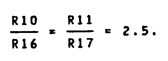
- A metering signal possibly applied to the input terminal MTCF of the SLIC is applied to the output SMI of OA4 via gating circuit GC,which has previously be unblocked,and OA4 and from there to the line via the amplifiers LOAD and LOA1 in the same way as described for the speech signal. However, in OA4 the metering signal is amplified by a factor equal to
or
- From the above it follows that a speech signal or a combined speech/metering signal superimposed on a DC loop current may flow in the line and hence in the feed resistances R0 and R1. This combined AC/DC current is detected by the sensing circuit SENC which provides at its output the voltage V5 given by the equation (5) or (9).
This output voltage V5 is applied to the DC feedback circuit DCFC wherein it is converted into a DC regulating voltage VEET connected to the like named voltage supply inputs VEET of the line amplifiers LOA0 and LOA1 which together with resistances R0, R1 and DCFC constitute a resistance synthesis circuit. The regulation of VEET corresponds to a conversion of each of the resistances R0 and R1 to a wanted resistance, as already explained in the above mentioned Belgian patent 898 049. - The output voltage V5 of the sensing circuit SENC is also used in an AC impedance synthesis circuit. Indeed, after DC has been removed from this output voltage by the capacitance C1 the resultant AC signal is applied via the amplifier stage OA3 to the line amplifiers LOA0 and LOA1. Amplifier stage OA3 may consist in an operational amplifier part of an overall SLIC integrated circuit design but with external components to determine the wanted complex impedance, e.g. a series input resistance and a feedback impedance comprising a resistance in series with another resistance shunted by a capacitance. Application of the OA3 output signal to LOA0 and LOA1 happens with opposite phases since the output of OA3, wherein V5 is multiplied by a wanted function, is connected tothe inverting input TAC of LOAD via resistance R12 and to the non-inverting input RDC of LOA1 through resistance R13. This AC feedback voltage signal is thus subtracted from the speech/metering voltage signal applied also with a opposite phases to the other inputs of these amplifiers via OA4, and the resulting error voltage signals after amplification by a gain factor

appears as a balanced push-pull signal between the line conductors LI0 and LI1. - With


each of the resistances R0 is converted into an impedance

the factor 2 resulting from the push-pull effect. Thus the total feed resistance R0 + R1 is converted into the impedance

when R0 = R1. - From the above it follows that the Herter bridge R0 - R5 is arranged at the junction of the unidirectional transmission and receive paths Tx and Rx and the bidirectional line LI0, LI1 and that it is used for the transmission of speech signals as well as of ringing signals although the latter have a much higher amplitude than the former. It is used,in combination with the comparator CO,for the detection of the closure of a hook switch contact during ringing or other instants. Finally, it is also used both in a resistance and in an impedance synthesis circuit.

Claims (8)
- Telecommunication line circuit including a pair of operational line amplifiers (LOA0, LOA1) coupled to first terminals (STA, SRB) of a pair of line feed resistances (R0, R1) whose second terminals (STB, STA) are coupled to a two-wire bi-directional line, said first and second pairs of terminals being coupled to a sensing circuit (SENC) which is able to sense the DC/AC current in said feed resistances and which together with said operational amplifier (LOA0, LOA1) is included in AC/DC feedback circuits enabling to synthesize desired characteristics and values of AC impedance and DC resistances from said AC/DC current feed resistances (R0, R1), and said first pair of terminals (STA, SRB) being moreover coupled to a generator (RS) of a ringing signal, characterized in that said sensing circuit (SENC) includes a Herter bridge (R0/R5) of which also said pair of line feed resistances (R0/R1) form part and which has an output (A, B) coupled to respective inputs of an operational sense amplifier (OA2), that said inputs (A, B) of said operational sense amplifier (OA2) are coupled to a first bias source (VAUX) through respective first bias resistances (R6, R7) and that the non-inverting input of said operational sense amplifier (OA2) is connected to a second bias source (VAG) through a second bias resistance (R9) whilst its output (CO1) is connected to its inverting input through a feedback third resistance (R8), all in such a manner that the AC/DC differential signal at the output (A, B) of the Herter bridge is converted to an AC/DC single-ended signal at the output of the operational amplifier (OA2) proportional to the sum of the signal drops across said feed resistances (R0, R1).
- Telecommunication line circuit according to claim 1, characterized in that the value of said second bias source (VAG) constitutes the reference output of said operational sense amplifier (OA2) in the absence of a sensed signal and that the value of said first bias source (VAUX) and of said first (R6, R7) second (R9) resistances have been so chosen that from a predermined wanted value

- Telecommunication line circuit according to claim 1, characterized in that the output (CO1) of said operational sense amplifier (OA2) is coupled to a DC level detection circuit (CO) through a signal path (R23, PG3, C3, PG4, PG2) which includes a filter circuit (R23, C2) for said ringing signal and which is unblocked (RNG=1) upon said ringing signal being applied across said first pair of terminals (STA, SRB).
- Telecommunication line circuit according to claim 3, characterized in that the output (CO1) of said operational sense amplifier (OA2) is also coupled to said DC level detection circuit (CO) through a second signal path (FC, OA6, PG1), which is unblocked (RNG=0) when no ringing signal is applied across said first pair of terminals (STA, SRB).
- Telecommunication line circuit according to claim 1, characterized in that said first pair of terminals (STA, SRB) is coupled to a receive leg (Rx) of a 4-wire exchange circuit, said receive leg being coupled to respective first push-pull inputs (TDC, RAC) of said two operational line amplifiers (LOAD, LOA1) and that the output of said operational sense amplifier (OA2) is capacitively (C1) coupled to respective second push-pull inputs (TAC, RDC) of said two operational line amplifiers, all in such a way that said AC impedance synthesis circuit is formed.
- Telecommunication line circuit according to claim 5, characterized in that the output (CO1) of said operational sense amplifier (OA2) is capacitively (CI) coupled to said second push-pull inputs (TAC, RDC) through an amplifier stage (OA3) including an impedance network determining the desired AC impedance to be synthesized, and that the output of said operational amplifier stage (OA3) is coupled (C2, R21, R22) to a transmit leg (Tx) of the 4-wire exchange.
- Telecommunication line circuit according to claim 6, characterized in that the output (CO1) of said operational sense amplifier (OA2) is coupled (DCFC) to voltage supply inputs (VEET) of said two operational line amplifiers (LOA0, LOA1) in such a way that a resistance synthesis circuit is formed.
- Telecommunication line circuit according to claim 7, characterized in that it includes second switching means (sw10/11) to disconnect said first pair of terminals (STA, SRB) from said receive leg (Rx) when switching means (sw30/31) connect said ringing generator (RC) to said first pair of terminals and vice-versa.
Priority Applications (8)
| Application Number | Priority Date | Filing Date | Title |
|---|---|---|---|
| AT85200774T ATE70681T1 (en) | 1985-05-17 | 1985-05-17 | TELECOMMUNICATION LINE CIRCUIT. |
| EP85200774A EP0201635B1 (en) | 1985-05-17 | 1985-05-17 | Telecommunication line circuit |
| DE8585200774T DE3584973D1 (en) | 1985-05-17 | 1985-05-17 | TELECOMMUNICATION CIRCUIT. |
| US06/852,609 US4837818A (en) | 1985-05-17 | 1986-04-16 | Telecommunication line circuit |
| AU57130/86A AU587823B2 (en) | 1985-05-17 | 1986-05-05 | Line circuit |
| BE2/60980A BE904786R (en) | 1985-05-17 | 1986-05-16 | TELECOMMUNICATION LINE CHAIN AND RELATED VOLTAGE CONVERTER. |
| ES555001A ES8708109A1 (en) | 1985-05-17 | 1986-05-16 | Telecommunication line circuit. |
| MX002534A MX168023B (en) | 1985-05-17 | 1986-05-16 | TELECOMMUNICATION LINE CIRCUIT |
Applications Claiming Priority (1)
| Application Number | Priority Date | Filing Date | Title |
|---|---|---|---|
| EP85200774A EP0201635B1 (en) | 1985-05-17 | 1985-05-17 | Telecommunication line circuit |
Publications (2)
| Publication Number | Publication Date |
|---|---|
| EP0201635A1 EP0201635A1 (en) | 1986-11-20 |
| EP0201635B1 true EP0201635B1 (en) | 1991-12-18 |
Family
ID=8194021
Family Applications (1)
| Application Number | Title | Priority Date | Filing Date |
|---|---|---|---|
| EP85200774A Expired EP0201635B1 (en) | 1985-05-17 | 1985-05-17 | Telecommunication line circuit |
Country Status (8)
| Country | Link |
|---|---|
| US (1) | US4837818A (en) |
| EP (1) | EP0201635B1 (en) |
| AT (1) | ATE70681T1 (en) |
| AU (1) | AU587823B2 (en) |
| BE (1) | BE904786R (en) |
| DE (1) | DE3584973D1 (en) |
| ES (1) | ES8708109A1 (en) |
| MX (1) | MX168023B (en) |
Families Citing this family (20)
| Publication number | Priority date | Publication date | Assignee | Title |
|---|---|---|---|---|
| US4897871A (en) * | 1980-04-04 | 1990-01-30 | Siemens Corporation | Apparatus for transmitting and/or receiving balanced signals on a two-wire telecommunication line |
| JPH088617B2 (en) * | 1988-09-19 | 1996-01-29 | 富士通株式会社 | Termination circuit in the power supply section of the electronic exchange |
| DE3884969T2 (en) * | 1988-12-24 | 1994-03-24 | Bell Telephone Mfg | MULTI-LOOP IMPEDANCE SYNTHESIS WITH FILTERS. |
| FR2642593B1 (en) * | 1989-01-31 | 1991-04-12 | Cit Alcatel | ELECTRONIC SUBSCRIBER LINE CONNECTION DEVICE |
| ATE110213T1 (en) * | 1989-09-27 | 1994-09-15 | Siemens Ag | SUBSCRIBER LINE CIRCUIT FOR CONNECTING A SUBSCRIBER LINE TO THE EXCHANGE OF A DIGITAL TIME-MULTIPLEX TELECOMMUNICATION SYSTEM. |
| DE69024947T2 (en) * | 1990-05-11 | 1996-08-08 | Alcatel Nv | Multiple loop impedance synthesis using filtering means |
| EP0455893B1 (en) * | 1990-05-11 | 1995-02-01 | Alcatel N.V. | Telecommunication line circuit |
| US5119365A (en) * | 1990-12-14 | 1992-06-02 | Ag Communication Systems Corporation | Bi-directional buffer line amplifier |
| US5511118A (en) * | 1991-01-31 | 1996-04-23 | Northern Telecom Limited | Method of providing d.c. feed to a telephone line |
| ES2111551T3 (en) * | 1991-12-16 | 1998-03-16 | Alsthom Cge Alcatel | SUITABLE AMPLIFIER POLARIZATION CIRCUIT FOR A CALL INTERRUPTION DETECTION SYSTEM. |
| DE69318551T2 (en) * | 1993-07-29 | 1998-09-10 | St Microelectronics Srl | Integrated subscriber line interface circuit with slow polarity switch |
| US5517565A (en) * | 1994-06-30 | 1996-05-14 | Harris Corporation | Integrated ringer relay circuit and method |
| US5694465A (en) * | 1995-03-16 | 1997-12-02 | Advanced Micro Devices, Inc. | Integrated ringer for short telephone lines |
| DE19636954B4 (en) * | 1996-09-11 | 2005-08-18 | Infineon Technologies Ag | subscriber circuit |
| FR2762177B1 (en) * | 1997-04-10 | 1999-05-14 | Schlumberger Ind Sa | ANALOG INTERFACE CIRCUIT FOR TELEPHONE EQUIPMENT |
| US6904174B1 (en) * | 1998-12-11 | 2005-06-07 | Intel Corporation | Simplified predictive video encoder |
| US7263127B1 (en) | 1998-04-02 | 2007-08-28 | Intel Corporation | Method and apparatus for simplifying frame-based motion estimation |
| US6628779B1 (en) | 1998-05-11 | 2003-09-30 | Telcordia Technologies, Inc. | Method and system for scaleable near-end speech cancellation for tip and ring tone signal detectors |
| US6930751B2 (en) * | 2001-01-11 | 2005-08-16 | Legerity, Inc. | Method and apparatus for reducing false hook detection |
| US20040076286A1 (en) * | 2002-10-16 | 2004-04-22 | Advanced Fibre Communication Inc. | Telephone circuit with a small, low-power ring trip monitor |
Family Cites Families (11)
| Publication number | Priority date | Publication date | Assignee | Title |
|---|---|---|---|---|
| BE754235A (en) * | 1969-08-05 | 1970-12-31 | Western Electric Co | SUPERVISION CIRCUIT FOR TELEPHONE LINES |
| FR2324181A1 (en) * | 1975-09-12 | 1977-04-08 | Lannionnais Electronique | Telephone line loop detector - has resistor bridge and amplifier to/ operating state of line connected to determine exchange or switchboard |
| US4387273A (en) * | 1980-08-25 | 1983-06-07 | International Telephone And Telegraph Corporation | Subscriber line interface circuit with impedance synthesizer |
| US4317963A (en) * | 1980-09-22 | 1982-03-02 | International Telephone And Telegraph Corporation | Subscriber line interface circuit utilizing impedance synthesizer and shared voltage source for loop current regulation control |
| US4396805A (en) * | 1981-09-21 | 1983-08-02 | Siemens Corporation | Ring trip detector for a subscriber line interface circuit |
| FR2527404B1 (en) * | 1982-05-19 | 1987-10-23 | Cit Alcatel | ELECTRONIC SUBSCRIBER |
| US4514595A (en) * | 1982-06-10 | 1985-04-30 | Northern Telecom Limited | Active impedance line feed circuit |
| US4539438A (en) * | 1983-08-22 | 1985-09-03 | Northern Telecom Limited | Active impedance transformer assisted line feed circuit with supervision filtering |
| BE898049A (en) * | 1983-10-21 | 1984-04-24 | Bell Telephone Mfg | TELECOMMUNICATION LINE CHAIN AND RELATED VOLTAGE CONVERTER. |
| US4532381A (en) * | 1984-02-13 | 1985-07-30 | Northern Telecom Limited | Active impedance line feed circuit |
| US4598173A (en) * | 1984-10-15 | 1986-07-01 | Itt Corporation | Interface circuit for a subscriber line circuit |
-
1985
- 1985-05-17 DE DE8585200774T patent/DE3584973D1/en not_active Expired - Lifetime
- 1985-05-17 EP EP85200774A patent/EP0201635B1/en not_active Expired
- 1985-05-17 AT AT85200774T patent/ATE70681T1/en not_active IP Right Cessation
-
1986
- 1986-04-16 US US06/852,609 patent/US4837818A/en not_active Expired - Fee Related
- 1986-05-05 AU AU57130/86A patent/AU587823B2/en not_active Ceased
- 1986-05-16 BE BE2/60980A patent/BE904786R/en not_active IP Right Cessation
- 1986-05-16 MX MX002534A patent/MX168023B/en unknown
- 1986-05-16 ES ES555001A patent/ES8708109A1/en not_active Expired
Also Published As
| Publication number | Publication date |
|---|---|
| AU587823B2 (en) | 1989-08-31 |
| DE3584973D1 (en) | 1992-01-30 |
| ES8708109A1 (en) | 1987-09-01 |
| AU5713086A (en) | 1986-11-20 |
| ES555001A0 (en) | 1987-09-01 |
| US4837818A (en) | 1989-06-06 |
| MX168023B (en) | 1993-04-29 |
| ATE70681T1 (en) | 1992-01-15 |
| BE904786R (en) | 1986-11-17 |
| EP0201635A1 (en) | 1986-11-20 |
Similar Documents
| Publication | Publication Date | Title |
|---|---|---|
| EP0201635B1 (en) | Telecommunication line circuit | |
| US5255317A (en) | Subscriber line interface circuit for serving ISDN subscribers using echo cancellers and POTS subscribers | |
| CA1096522A (en) | Subscriber line-trunk circuit | |
| CA1292588C (en) | Subscriber line interface circuit | |
| US4472608A (en) | Subscriber line interface circuit | |
| US5329588A (en) | Telecommunication line circuit | |
| NZ226249A (en) | Line interface: resistive bridge input | |
| US5274702A (en) | Wideband telephone line interface circuit | |
| US4866768A (en) | Station line interface circuit for a telecommunication network | |
| JPH06502046A (en) | line interface circuit | |
| CA2042292C (en) | Impedance synthesis multiple loop using filtering means | |
| US4281219A (en) | Telephone line circuit | |
| GB2149618A (en) | Telecommunication line circuit and associated voltage converter | |
| NO153590B (en) | CONNECT LINE INTERFACE FOR CONNECTING A TWO-LINE CONNECTION LINE WITH A PHONE CENTER. | |
| JPS5912638A (en) | Impedance synthesis type line circuit | |
| GB2193063A (en) | Line circuits | |
| EP0237656B1 (en) | Telecommunication line circuit and amplifier circuit used therein | |
| JPS6230546B2 (en) | ||
| EP0241604A2 (en) | Polarity reversal circuit | |
| FI104933B (en) | SLIC | |
| GB2055021A (en) | Telephone line circuit | |
| US4087645A (en) | Telephone switching system | |
| CA2205320C (en) | Telephone line interface circuit with voltage control | |
| KR0116914Y1 (en) | Electronic exchange | |
| EP0089350A4 (en) | Electronic terminator circuit. |
Legal Events
| Date | Code | Title | Description |
|---|---|---|---|
| PUAI | Public reference made under article 153(3) epc to a published international application that has entered the european phase |
Free format text: ORIGINAL CODE: 0009012 |
|
| AK | Designated contracting states |
Kind code of ref document: A1 Designated state(s): AT BE CH DE FR GB IT LI LU NL SE |
|
| RBV | Designated contracting states (corrected) |
Designated state(s): AT CH DE FR GB IT LI NL |
|
| 17P | Request for examination filed |
Effective date: 19870512 |
|
| RAP1 | Party data changed (applicant data changed or rights of an application transferred) |
Owner name: ALCATEL N.V. Owner name: BELL TELEPHONE MANUFACTURING COMPANY NAAMLOZE VENN |
|
| RAP3 | Party data changed (applicant data changed or rights of an application transferred) |
Owner name: ALCATEL N.V. Owner name: BELL TELEPHONE MANUFACTURING COMPANY NAAMLOZE VENN |
|
| 17Q | First examination report despatched |
Effective date: 19890615 |
|
| ITF | It: translation for a ep patent filed | ||
| GRAA | (expected) grant |
Free format text: ORIGINAL CODE: 0009210 |
|
| AK | Designated contracting states |
Kind code of ref document: B1 Designated state(s): AT CH DE FR GB IT LI NL |
|
| REF | Corresponds to: |
Ref document number: 70681 Country of ref document: AT Date of ref document: 19920115 Kind code of ref document: T |
|
| ET | Fr: translation filed | ||
| REF | Corresponds to: |
Ref document number: 3584973 Country of ref document: DE Date of ref document: 19920130 |
|
| PLBE | No opposition filed within time limit |
Free format text: ORIGINAL CODE: 0009261 |
|
| STAA | Information on the status of an ep patent application or granted ep patent |
Free format text: STATUS: NO OPPOSITION FILED WITHIN TIME LIMIT |
|
| 26N | No opposition filed | ||
| PGFP | Annual fee paid to national office [announced via postgrant information from national office to epo] |
Ref country code: DE Payment date: 19930716 Year of fee payment: 9 |
|
| PGFP | Annual fee paid to national office [announced via postgrant information from national office to epo] |
Ref country code: CH Payment date: 19930813 Year of fee payment: 9 |
|
| NLS | Nl: assignments of ep-patents |
Owner name: ALCATEL N.V. TE AMSTERDAM. |
|
| PG25 | Lapsed in a contracting state [announced via postgrant information from national office to epo] |
Ref country code: LI Effective date: 19940531 Ref country code: CH Effective date: 19940531 |
|
| REG | Reference to a national code |
Ref country code: CH Ref legal event code: PL |
|
| PG25 | Lapsed in a contracting state [announced via postgrant information from national office to epo] |
Ref country code: DE Effective date: 19950201 |
|
| PGFP | Annual fee paid to national office [announced via postgrant information from national office to epo] |
Ref country code: AT Payment date: 19950508 Year of fee payment: 11 |
|
| PG25 | Lapsed in a contracting state [announced via postgrant information from national office to epo] |
Ref country code: AT Effective date: 19960517 |
|
| PGFP | Annual fee paid to national office [announced via postgrant information from national office to epo] |
Ref country code: GB Payment date: 19980414 Year of fee payment: 14 |
|
| PGFP | Annual fee paid to national office [announced via postgrant information from national office to epo] |
Ref country code: FR Payment date: 19980417 Year of fee payment: 14 |
|
| PGFP | Annual fee paid to national office [announced via postgrant information from national office to epo] |
Ref country code: NL Payment date: 19980430 Year of fee payment: 14 |
|
| PG25 | Lapsed in a contracting state [announced via postgrant information from national office to epo] |
Ref country code: GB Free format text: LAPSE BECAUSE OF NON-PAYMENT OF DUE FEES Effective date: 19990517 |
|
| PG25 | Lapsed in a contracting state [announced via postgrant information from national office to epo] |
Ref country code: NL Free format text: LAPSE BECAUSE OF NON-PAYMENT OF DUE FEES Effective date: 19991201 |
|
| GBPC | Gb: european patent ceased through non-payment of renewal fee |
Effective date: 19990517 |
|
| PG25 | Lapsed in a contracting state [announced via postgrant information from national office to epo] |
Ref country code: FR Free format text: LAPSE BECAUSE OF NON-PAYMENT OF DUE FEES Effective date: 20000131 |
|
| NLV4 | Nl: lapsed or anulled due to non-payment of the annual fee |
Effective date: 19991201 |
|
| REG | Reference to a national code |
Ref country code: FR Ref legal event code: ST |