EP0200480A2 - Non-volatile memory cell and non-volatile random access memory cell utilising the same - Google Patents
Non-volatile memory cell and non-volatile random access memory cell utilising the same Download PDFInfo
- Publication number
- EP0200480A2 EP0200480A2 EP86303102A EP86303102A EP0200480A2 EP 0200480 A2 EP0200480 A2 EP 0200480A2 EP 86303102 A EP86303102 A EP 86303102A EP 86303102 A EP86303102 A EP 86303102A EP 0200480 A2 EP0200480 A2 EP 0200480A2
- Authority
- EP
- European Patent Office
- Prior art keywords
- capacitor
- transistor
- memory cell
- node
- tunnel
- Prior art date
- Legal status (The legal status is an assumption and is not a legal conclusion. Google has not performed a legal analysis and makes no representation as to the accuracy of the status listed.)
- Withdrawn
Links
Images
Classifications
-
- G—PHYSICS
- G11—INFORMATION STORAGE
- G11C—STATIC STORES
- G11C14/00—Digital stores characterised by arrangements of cells having volatile and non-volatile storage properties for back-up when the power is down
Definitions
- the present invention relates to a non-volatile memory cell and non-volatile random access memory (NVRAM) cell utilising the same.
- NVRAM non-volatile random access memory
- an SRAM cell has the advantage that the access time is short and the data can be re-written without limitation, but a disadvantage is that the cell is volatile.
- an EEPROM cell has the advantage that it is non-volatile, but the disadvantage that a long access time is required and the number of times data can be re-written is limited.
- the data can be written into or read out from the NVRAM cell in a short time, and also the data can be re-written without any limitation.
- the power supply voltage of the NVRAM cell is turned off, using advantageous properties the / of the EEPROM cell, the data in the SRAM cell portion can be stored in the EEPROM cell portion, and the data stored in the EEPROM cell portion can be recalled to the SRAM cell portion when the power supply voltage is disadvantage turned on.
- the / of the long access time of the EEPROM cell has little effect on the NVRAM cell because the the data access is required only for/short time whilst the power supply voltage of the NVRAM cell is turned on and off.
- the NVRAM cell has a-problem that its size becomes large; accordingly, proposals have been made to reduce the cell size for increasing the packing density of a memory device consisting of NVRAM cells.
- the SRAM cell portion therein simply consists of a few components of a flip-flop circuit, so that the EEPROM cell portion therein becomes a subject for increasing the packing density of the NVRAM cell.
- the U.S. Patent Appln. S.N. 659,191 invented by the inventor of the present invention gave a solution to the above problem by increasing the packing density of the EEPROM cell portion.
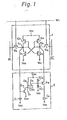
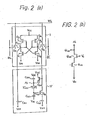
- a prior of the accompanying drawings art NVRAM cell is such as shown in Fig. 1/ and an NVRAM that cell proposed in/ Patent Application is such as shown in Fig. 2(a).
- the NVRAM cell functions as a memory matrix element of a memory device, wherein the a element is designated by/respective word line WL and respective pair of bit lines BL and BL of the memory device.
- the NVRAM cell of Fig. 1 consists of an SRAM cell portion 1 and an EEPROM cell portion 2 and the NVRAM cell of Fig. 2(a) consists of an SRAM cell portion 1 and an EEPROM cell portion 17; the SRAM cell portions 1 of Figs. 1 and 2(a) are the same. Comparing Figs. 1 and 2(a), it can be seen that the improvement of the packing density of the NVR A M cell is achieved by reducing the circuit components of the EEPROM cell portion 2.
- FIG. 2(b) shows a modified partial circuit of Fig. 2(a); i.e., in Fig. 2(b), instead of removing the capacitor C 62 in Fig. 2(a), a control transistor Q 100 is placed between the node N 2 and the transistor Q 61 .
- the details of the function of the NVRAM cell in Figs. 1 , 2(a) and 2(b) are well discussed in U.S. Patent Appln. S.N. 659,191, so the explanation of these details is not repeated here.
- the NVRAM cell shown in Fig. 2(a) is most useful, because, as seen from Fig. 2(a), the NVRAM cell of Fig. 2(a) has the structure of removing the connection between the node N 1 of the SRAM cell portion 1 and the circuit of the EEPROM cell portion 2, so that the NVRAM cell of Fig. 2(a) is effective not only for increasing the packing density of the NVRAM cell but also for increasing the freedom for design of the structure of the NVRAM cell.
- the EEPROM cell portion 17 operates with two kinds of power sources V H1 and V H2 .
- the two kinds of power sources make the peripheral circuitry of the NVRAM cell a little more complicated, (which, however, is not so negative factor for the NVRAM cell of Fig. 2(a)).
- the two kinds of power supply voltage bring new problems to the NVRAM cell of Fig. 2(a) as follows.
- a non-volatile memory cell comprising:
- a non-volatile random-access memory cell by combining the non-volatile memory cell of the preceding paragraph with a volatile memory cell comprising:
- An embodiment of the present invention may provide an NVRAM cell constituted by a volatile static type random-access memory (SRAM) cell portion and a non-volatile electrically erasable programmable read-only memory (EEPROM) cell portion.
- SRAM static type random-access memory
- EEPROM electrically erasable programmable read-only memory
- An embodiment of the present invention may increase the packing density of a memory device consisting of NVRAM cells whilst keeping the reliability high.
- An embodiment of the present invention may give more freedom in the design of the semiconductor structure of the NVRAM cell.
- An embodiment of the present invention may increase the yield rate of production of memory devices consisting of NVRAM cells.
- An embodiment of the present invention may reduce the time for storing or re-calling data into or out from the EEPROM cell portion of an NVRAM cell.
- An embodiment of the present invention may increase the life of an NVRAM cell.
- An embodiment of the present invention may provide an NVRAM cell in which repetition of the charging for storing a datum (item of data) can be made any number of times.
- an improved EEPROM cell portion combined with an SRAM cell portion.
- the improved EEPROM cell portion operates under only one power supply voltage called a writing voltage when the power supply-voltage for the SRAM cell portion is intended to be turned off.
- the improved EEPROM cell portion comprises:a memory transistor having a floating gate on which charge is stored such that the polarity of the charge is determined in correspondence with the level of the bit signal at one node of the flip-flop circuit in the SRAM cell portion; a capacitor circuit comprising a tunnel capacitor; and two transistors for controlling the polarity of the charge being stored at the floating gate in cooperation with a tunnel current of the tunnel capacitor.
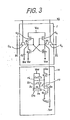
- Fig. 3 shows a circuit diagram of an NVRAM cell embodying the present invention.
- the NVRAM cell consists of an SRAM cell portion 1, which may be the same as SRAM cell portion 1 in Fig. 1 or 2(a), and an EEPROM cell portion 20.
- a plurality of the NVRAM cells 1 form a memory device (an NVRAM device) having the structure of a memory matrix, and a each NVRAM cell is designated by/respective word-line WL and respective pair of bit-lines BL and BL.
- the SRAM cell portion 1 comprises four metal insulator semiconductor (MIS) transistors Q 1 , Q 2 , Q 3 , and Q 4 (the transistors Q 1 and Q 2 are the ordinary enhancement type, and the transistors Q 3 and Q 4 are the depletion type which are distinguished from the enhancement type in the Figure by a black dot) which are cross-coupled at nodes N 1 and N 2 forming an ordinary data flip-flop circuit.
- MIS metal insulator semiconductor
- the EEPROM cell portion 20 is a non-volatile memory cell which comprises a memory MIS transistor Q 8 having a floating gate FG, the MIS transistors Q 7 and Q 11 , and a capacitor circuit consisting of a capacitor module CM 2 , capacitors C 4 and C 5 , and tunnel capacitor TC 3 .
- the capacitor module C M2 , the tunnel capacitor TC 3 , and the capacitor C 5 are made from depletion type MIS shown their transistors (each/having a black dot)each having/ drain and source connected together.
- the capacitor module CM 2 has static capacitance between a between common electrode D 4 and an electrode D 5 and/the common electrode D 4 and an electrode D 6 ;
- the tunnel capacitor TC 3 which can is a capacitor/function by a tunnel effect and whose (relatively small) capacitance is selected so as to be sufficiently small/ compared with the capacitance of the capacitor module CM 2 and the capacitor C 5 ;
- the capacitor C 4 is selected to have a value sufficiently large compared with-that of the capacitor C 3 of the S RA M cell portion 1.
- the transistors Q 7 and Q 11 each function as a switch corresponding to a signal level H or L applied to the gate; however, they operate oppositely to each other, i.e., the transistor Q 11 switches OFF and ON corresponding to ON and OFF operations of the transistor Q 7 .
- this NVRAM cell embodying the present the invention is divided into/following modes: (1).Store Mode 1 held (The mode of storing a datum held in the SRAM cell portion 1 into the EEPROM cell portion 20 when the potential at the node N 1 is L and that at the node N 2 is H), (2) Store Mode 2 (The store mode when the potential at the node N 1 is H and that at the node N 2 is L), (3) Recall Mode 1 (The mode of recalling the data stored in the EEPROM cell portion 20 back to the SRAM cell portion 1 when a negative charge is stored at the floating gate FG of the transistor Q 8 ), and (4) Recall Mode 2 (The same recall mode but when a positive charge is stored at floating gate these FG).
- the NVRAM cell operates as follows. (1) Store Mode 1 is raised
- V voltage at the node N 2
- the transistor Q 7 is ON (reference symbol V SS is a low potential such as earth potential), so that the potential at the node N 4 becomes L and the transistor Q 11 becomes OFF.
- the writing voltage V HH is applied to a series circuit consisting of the capacitor formed between the electrodes D 4 and D 5 , the capacitor formed between the electrodes D 4 and D 6 , and the tunnel capacitor TC 3 .
- the static capacitance of the capacitor module CM 2 is sufficiently larger than greater that of the tunnel capacitor TC 3 so that the/ part of the writing voltage V HH is applied to the tunnel capacitor TC 3 .
- electrons move from the node N 4 to.the floating gate FG of the transistor Q 8 through the tunnel capacitor TC 3 by the tunnel effect, so that a negative charge is stored at the floating gate FG, which makes the transistor Q 8 OFF, and the negative charge stored at the floating gate FG is retained for a long period, even though the power supply voltage V CC and the writing voltage V HH are turned off.
- the transistor Q 8 is called a memory transistor.
- the transistor Q 8 Since the potential at the node N 2 is L, the transistor Q 8 becomes OFF, so that the node N 4 goes into a floating state; however, when the writing voltage V HH is applied, the potential at the node N 4 risesup, which turns ON the transistor Q 11 . Accordingly, the writing voltage V HH is applied to the series circuit consisting of the capacitor C 5 , the tunnel capacitor TC 3 , and the capacitor formed between the electrodes D 4 and D 6 . Thus the greater part of the writing voltage V HH is applied to the tunnel capacitor TC 3 ,because the capacitance of the tunnel the capacitor is sufficiently small compared with/other capacitance of the capacitors in the series circuit as mentioned before.
- the power supply voltage V CC for the memory is set cell 1 is set to 0 V.
- the transistor Q 8 is cut off, disconnecting the connection between the node N 2 and the capacitor C 4 . Therefore, when the power supply voltage V CC (5 V) is turned on, since the capacitor C 3 is connected to the node N 1 and the capacitor C 4 is disconnected from the node N 2' the potential at the node N 1 becomes L because only the load at the node N 1 is heavy, and the potential at the node N 2 becomes H.
- the data stored in the EEPROM cell portion 20 is recalled to the NVRAM cell when the power supply voltage is turned on.
- the power supply voltage V CC for the memory is set cell 1/to 0 V.
- a positive charge exists at the floating gate FG, so that the transistor Q 8 is ON connecting the node N 2 to the capacitor C 4 . Therefore, when the power supply voltage V CC (5 V) is turned on, since the capacitance of the capacitor C 4 is selected so as to be larger than that of the capacitor C 3 , the flip-flop circuit in the SRAM cell portion 1 functions so that the potential at the N 1 becomes H and that at the N 2 becomes L.
- the data stored in the EEPROM cell portion 20 is recalled to the NVRAM cell when the power supply voltage is turned on.
- the EEPROM cell portion 20 uses only one writing voltage V HH ; therefore, which the it does not share the problems/ NVRAM cell, shown in Fig. 2, had . That is, the problems of the previously proposed NVRAM cell taking too much time to store and recall data, having a short life and being difficult to give enough holding time, may all be solved in this embodiment of the present invention.
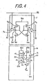
- Fig. 4 is a circuit diagram of an NVRAM cell showing another embodiment of the present invention.
- the function and the operation of Fig. 4 are similar to those of Fig. 3.
- the circuit from the node N 2 to the earth potential V SS through the transistor Q 8 and the capacitor similar way C 5 in Fig. 3 is modified in a to the modified partial circuit shown in Fig. 2(b); i.e., the capacitor C 4 in Fig. 3 is omitted, and a control transistor Q 10 is placed between the node N 2 and the transistor Q 8 for switching the connection between the node N 2 and the memory transistor Q 8 ; the switching action is made by a control voltage V c applied to the gate of the transistor Q 10 .
- an embodiment of the present invention provides / a non-volatile random access memory (NVRAM) cell includ.ing a volatile static type random access memory cell consisting of a flop-flip circuit having two nodes on which a paired bit signal may be accessed and a non-volatile electrically erasable programmable read-only memory (EEPROM) cell consisting of a memory transistor having a floating gate, a capacitor circuit, to which a voltage called a writing voltage is applied, including a tunnel capacitor, and two transistors for determining the polarity S of charge to be stored at the floating gate with a tunnel current in the tunnel capacitor corresponding to the level of the bit signal existing at one of the two nodes in the flip-flop circuit.
- NVRAM non-volatile random access memory
- EEPROM electrically erasable programmable read-only memory
- the EEPROM cell When the power supply voltage of the NVRAM cell is turned off, the EEPROM cell stores the positive or negative charge at the floating gate corresponding to the bit signal level at the node in the flip-flop circuit holding the charge after the power supply voltage and the writing voltage are turned off. When the power supply voltage is turned on, the EEPROM cell recalls the the the state of the flip-flop circuit so as to be/same as before using the charge stored at the floating gate.
Landscapes
- Static Random-Access Memory (AREA)
- Semiconductor Memories (AREA)
Abstract
Description
- The present invention relates to a non-volatile memory cell and non-volatile random access memory (NVRAM) cell utilising the same.
- Generally, in the art of semiconductor memory devices, an ideal semiconductor memory device has been awaited such that data can be re-written therein without limitation, access thereto can be made in a short time, and of a non-volatile type.
- Generally, an SRAM cell has the advantage that the access time is short and the data can be re-written without limitation, but a disadvantage is that the cell is volatile. On the contrary, an EEPROM cell has the advantage that it is non-volatile, but the disadvantage that a long access time is required and the number of times data can be re-written is limited.
- In an attempt to realize such an ideal semiconductor memory device, recently, an NVRAM cell has been proposed which combines the merits (properties) of the SRAM cell and the EEPROM cell. When the power supply voltage of the NVRAM cell is ON, using the advantageous properties
- / of the SRAM cell, the data can be written into or read out from the NVRAM cell in a short time, and also the data can be re-written without any limitation. When the power supply voltage of the NVRAM cell is turned off, using advantageous properties the / of the EEPROM cell, the data in the SRAM cell portion can be stored in the EEPROM cell portion, and the data stored in the EEPROM cell portion can be recalled to the SRAM cell portion when the power supply voltage is disadvantage turned on. The / of the long access time of the EEPROM cell has little effect on the NVRAM cell because the the data access is required only for/short time whilst the power supply voltage of the NVRAM cell is turned on and off.
- - However, the NVRAM cell has a-problem that its size becomes large; accordingly, proposals have been made to reduce the cell size for increasing the packing density of a memory device consisting of NVRAM cells. In the NVRAM cell, the SRAM cell portion therein simply consists of a few components of a flip-flop circuit, so that the EEPROM cell portion therein becomes a subject for increasing the packing density of the NVRAM cell. The U.S. Patent Appln. S.N. 659,191 invented by the inventor of the present invention gave a solution to the above problem by increasing the packing density of the EEPROM cell portion. According to the U.S. Patent Appln. S.N. 659,191, a prior of the accompanying drawings art NVRAM cell is such as shown in Fig. 1/ and an NVRAM that cell proposed in/ Patent Application is such as shown in Fig. 2(a).
- In Fig. 1 or 2(a), the NVRAM cell functions as a memory matrix element of a memory device, wherein the a element is designated by/respective word line WL and respective pair of bit lines BL and BL of the memory device. The NVRAM cell of Fig. 1 consists of an
SRAM cell portion 1 and anEEPROM cell portion 2 and the NVRAM cell of Fig. 2(a) consists of anSRAM cell portion 1 and anEEPROM cell portion 17; theSRAM cell portions 1 of Figs. 1 and 2(a) are the same. Comparing Figs. 1 and 2(a), it can be seen that the improvement of the packing density of the NVRAM cell is achieved by reducing the circuit components of theEEPROM cell portion 2. Fig. 2(b) shows a modified partial circuit of Fig. 2(a); i.e., in Fig. 2(b), instead of removing the capacitor C62 in Fig. 2(a), a control transistor Q100 is placed between the node N2 and the transistor Q61. The details of the function of the NVRAM cell in Figs. 1 , 2(a) and 2(b) are well discussed in U.S. Patent Appln. S.N. 659,191, so the explanation of these details is not repeated here. - In the U.S. Patent Appln. S.N. 659,191, many embodiments were disclosed-, but in practice
the NVRAM cell shown in Fig. 2(a) is most useful, because, as seen from Fig. 2(a), the NVRAM cell of Fig. 2(a) has the structure of removing the connection between the node N1 of theSRAM cell portion 1 and the circuit of theEEPROM cell portion 2, so that the NVRAM cell of Fig. 2(a) is effective not only for increasing the packing density of the NVRAM cell but also for increasing the freedom for design of the structure of the NVRAM cell. However, as shown in Fig. 2(a), theEEPROM cell portion 17 operates with two kinds of power sources VH1 and VH2. The two kinds of power sources make the peripheral circuitry of the NVRAM cell a little more complicated, (which, however, is not so negative factor for the NVRAM cell of Fig. 2(a)). The two kinds of power supply voltage bring new problems to the NVRAM cell of Fig. 2(a) as follows. - (1) Two steps such as "pre-set" and "set" are necessary every time the floating gate FG62 of the transistor Q61 in the
EEPROM cell portion 17 is charged or discharged for storing data, so that it takes a relatively long time to store the data. - (2) When a memory device consisting of a plurality of NVRAM cells is used as a read only memory (ROM) device, the two steps of "pre-set" and "set" must be out carried/ every time data is stored and recalled; accordingly, the life of the memory device is reduced. And,
- (3) in a semiconductor device, a PN junction generally produces a leakage current, e.g., the leakage current flows at a node N3 in Fig. 2(a), so that the holding time, which should be long for the NVRAM cell, of the capacitance-coupling-charge becomes short when the temperature at the PN junction increases. Therefore, repeating the charging of the floating gate again and again is necessary for lengthening the apparent holding time under the consideration of the upper allowable limit of the temperature characteristic of the NVRAM cell. However, the repeated charging cannot be carried out in the NVRAM cell of Fig. 2(a), because the floating gate FG62 is always discharged every time new data is going to be stored in the
EEPROM cell portion 17. - According to one aspect of the present invention there is provided a non-volatile memory cell comprising:
- a memory transistor having a floating gate, operable to act as a switch in accordance wi.th the polarity of a charge stored at said floating gate;
- a capacitor circuit comprising a tunnel capacitor operatively connected to said floating gate;
- means, operatively connected to said capacitor circuit, for applying a writing voltage having an amplitude large enough to cause a tunnel current to flow through said tunnel capacitor,
- a first transistor, operatively connected to an input/output node of the cell and to said capacitor circuit, for controlling the polarity of said tunnel current in accordance with a data signal from said input/output node, said first transistor generating an output in response to said data signal;
- a second transistor, operatively connected to said capacitor circuit receiving the output of said first transistor, for controlling the polarity of said tunnel current in accordance with said data signal;
- said first and second transistors cooperatively controlling the polarity of the tunnel current when said writing voltage is applied to said capacitor circuit, one of said first and second transistors being ON and the other being OFF when said tunnel current is to flow, said polarity of the tunnel current being controlled to be in one of two directions depending on which one of said first and second transistors is ON, said two directions being such that said floating gate is provided with either a negative or a positive charge by said tunnel current, so as to store data corresponding to the data signal.
- According to a further aspect or development of the invention, there is provided a non-volatile random-access memory cell by combining the non-volatile memory cell of the preceding paragraph with a volatile memory cell comprising:
- a flip-flap circuit having firs.t and second nodes from which, in use, complementary data signals corresponding to data stored in the volatile memory cell are output, and
- a capacitor connected to the first node;
- wherein the second node of the volatile memory cell is connected to the input/output node of the non-volatile memory cell, whereby data can be transferred between the volatile memory cell and the non-volatile memory cell.
- Further aspects of the invention provide non-volatile random access memory cells as defined in claims 5 and 6.
- An embodiment of the present invention may provide an NVRAM cell constituted by a volatile static type random-access memory (SRAM) cell portion and a non-volatile electrically erasable programmable read-only memory (EEPROM) cell portion.
- An embodiment of the present invention may increase the packing density of a memory device consisting of NVRAM cells whilst keeping the reliability high.
- An embodiment of the present invention may give more freedom in the design of the semiconductor structure of the NVRAM cell.
- An embodiment of the present invention may increase the yield rate of production of memory devices consisting of NVRAM cells.
- An embodiment of the present invention may reduce the time for storing or re-calling data into or out from the EEPROM cell portion of an NVRAM cell.
- An embodiment of the present invention may increase the life of an NVRAM cell.
- An embodiment of the present invention may provide an NVRAM cell in which repetition of the charging for storing a datum (item of data) can be made any number of times. embodiments
- In / of the present invention there may be provided an improved EEPROM cell portion combined with an SRAM cell portion. The improved EEPROM cell portion operates under only one power supply voltage called a writing voltage when the power supply-voltage for the SRAM cell portion is intended to be turned off. The improved EEPROM cell portion comprises:a memory transistor having a floating gate on which charge is stored such that the polarity of the charge is determined in correspondence with the level of the bit signal at one node of the flip-flop circuit in the SRAM cell portion; a capacitor circuit comprising a tunnel capacitor; and two transistors for controlling the polarity of the charge being stored at the floating gate in cooperation with a tunnel current of the tunnel capacitor.
- Reference is made, by way of example, to the accompanying drawings in which:
- previously proposed Fig. I is a circuit diagram of a previously proposed NVRAM cell;
- Fig. 2(a) is a circuit diagram of another / NVRAM cell;
- Fig. 2(b) is a modified partial circuit of Fig. 2(a);
- Fig. 3 is a circuit diagram embodying the present invention; and
- Fig. 4 is another circuit diagram embodying the present invention.
- Fig. 3 shows a circuit diagram of an NVRAM cell embodying the present invention. In Fig. 3, the same reference numerals and symbols as in Figs. 1 and 2(a) to those designate similar elements or parts/ in Figs. 1 and 2(a). The NVRAM cell consists of an
SRAM cell portion 1, which may be the same asSRAM cell portion 1 in Fig. 1 or 2(a), and anEEPROM cell portion 20. A plurality of theNVRAM cells 1 form a memory device (an NVRAM device) having the structure of a memory matrix, and a each NVRAM cell is designated by/respective word-line WL and respective pair of bit-lines BL and BL. - The
SRAM cell portion 1 comprises four metal insulator semiconductor (MIS) transistors Q1, Q2, Q3, and Q4 (the transistors Q1 and Q2 are the ordinary enhancement type, and the transistors Q3 and Q4 are the depletion type which are distinguished from the enhancement type in the Figure by a black dot) which are cross-coupled at nodes N1 and N2 forming an ordinary data flip-flop circuit. Complementary/signals such as a paired bit signals are written into the flip-flop circuit from the bit-lines BL and BL or read out from the flip-flop circuit to the bit-lines BL and BE through two transfer gate MIS transistors QG connected to the nodes N1 and N2. - The
EEPROM cell portion 20 is a non-volatile memory cell which comprises a memory MIS transistor Q8 having a floating gate FG, the MIS transistors Q7 and Q11, and a capacitor circuit consisting of a capacitor module CM2, capacitors C4 and C5, and tunnel capacitor TC3. The capacitor module CM2, the tunnel capacitor TC3, and the capacitor C5 are made from depletion type MIS shown their transistors (each/having a black dot)each having/ drain and source connected together. The capacitor module CM2 has static capacitance between a between common electrode D4 and an electrode D5 and/the common electrode D4 and an electrode D6; the tunnel capacitor TC3 which can is a capacitor/function by a tunnel effect and whose (relatively small) capacitance is selected so as to be sufficiently small/ compared with the capacitance of the capacitor module CM2 and the capacitor C5; and the capacitor C4 is selected to have a value sufficiently large compared with-that of the capacitor C3 of the SRAM cell portion 1. The transistors Q7 and Q11 each function as a switch corresponding to a signal level H or L applied to the gate; however, they operate oppositely to each other, i.e., the transistor Q11 switches OFF and ON corresponding to ON and OFF operations of the transistor Q7. - The operation of this NVRAM cell embodying the present the invention is divided into/following modes: (1
).Store Mode 1 held (The mode of storing a datum held in theSRAM cell portion 1 into theEEPROM cell portion 20 when the potential at the node N1 is L and that at the node N2 is H), (2) Store Mode 2 (The store mode when the potential at the node N1 is H and that at the node N2 is L), (3) Recall Mode 1 (The mode of recalling the data stored in theEEPROM cell portion 20 back to theSRAM cell portion 1 when a negative charge is stored at the floating gate FG of the transistor Q8), and (4) Recall Mode 2 (The same recall mode but when a positive charge is stored at floating gate these FG). In / modes, the NVRAM cell operates as follows. (1)Store Mode 1 is raised - The writing voltage VHH/up to 20 - 30 volt (V) from 0 V, before turning the power supply voltage VCC off. At this time, since the voltage at the node N2 is "H", the transistor Q7 is ON (reference symbol VSS is a low potential such as earth potential), so that the potential at the node N4 becomes L and the transistor Q11 becomes OFF. Accordingly, the writing voltage VHH is applied to a series circuit consisting of the capacitor formed between the electrodes D4 and D5, the capacitor formed between the electrodes D4 and D6, and the tunnel capacitor TC3. As mentioned before, the static capacitance of the capacitor module CM2 is sufficiently larger than greater that of the tunnel capacitor TC3 so that the/ part of the writing voltage VHH is applied to the tunnel capacitor TC3. At this time, electrons move from the node N4 to.the floating gate FG of the transistor Q8 through the tunnel capacitor TC3 by the tunnel effect, so that a negative charge is stored at the floating gate FG, which makes the transistor Q8 OFF, and the negative charge stored at the floating gate FG is retained for a long period, even though the power supply voltage VCC and the writing voltage VHH are turned off. Thus, the data in the
SRAM cell portion 1 can be completely stored in- theEEPROM cell portion 20. From the above, the transistor Q 8 is called a memory transistor. - Since the potential at the node N2 is L, the transistor Q8 becomes OFF, so that the node N4 goes into a floating state; however, when the writing voltage VHH is applied, the potential at the node N4 risesup, which turns ON the transistor Q11 . Accordingly, the writing voltage VHH is applied to the series circuit consisting of the capacitor C5, the tunnel capacitor TC3, and the capacitor formed between the electrodes D4 and D6. Thus the greater part of the writing voltage VHH is applied to the tunnel capacitor TC3,because the capacitance of the tunnel the capacitor is sufficiently small compared with/other capacitance of the capacitors in the series circuit as mentioned before. In this case, since the potential at the N4 is higher than that at the floating gate FG, the electrons which existed at the floating gate FG are extracted by the tunnel effect of the tunnel capacitor TC3; accordingly, a positive charge is stored at the floating gate FG making the transistor Q8 ON. The positive charge stored at the floating gate FG is retained for a long period. Thus, the data in the
SRAM cell portion 1 can be completely stored into theEEPROM cell portion 20. - First, the power supply voltage VCC for the memory is set
cell 1 is set to 0 V. At this time, since a negative charge exists at the floating gate FG, the transistor Q8 is cut off, disconnecting the connection between the node N2 and the capacitor C4. Therefore, when the power supply voltage VCC (5 V) is turned on, since the capacitor C3 is connected to the node N1 and the capacitor C4 is disconnected from the node N2' the potential at the node N1 becomes L because only the load at the node N1 is heavy, and the potential at the node N2 becomes H.- Thus, the data stored in theEEPROM cell portion 20 is recalled to the NVRAM cell when the power supply voltage is turned on. - First, the power supply voltage VCC for the memory is set
cell 1/to 0 V. At this time, a positive charge exists at the floating gate FG, so that the transistor Q8 is ON connecting the node N2 to the capacitor C4. Therefore, when the power supply voltage VCC (5 V) is turned on, since the capacitance of the capacitor C4 is selected so as to be larger than that of the capacitor C3, the flip-flop circuit in theSRAM cell portion 1 functions so that the potential at the N1 becomes H and that at the N2 becomes L. Thus, the data stored in theEEPROM cell portion 20 is recalled to the NVRAM cell when the power supply voltage is turned on. - As seen from the above discussion, the
EEPROM cell portion 20 uses only one writing voltage VHH; therefore, which the it does not share the problems/ NVRAM cell, shown in Fig. 2, had . That is, the problems of the previously proposed NVRAM cell taking too much time to store and recall data, having a short life and being difficult to give enough holding time, may all be solved in this embodiment of the present invention. - Fig. 4 is a circuit diagram of an NVRAM cell showing another embodiment of the present invention. The function and the operation of Fig. 4 are similar to those of Fig. 3. In Fig. 4, the circuit from the node N2 to the earth potential VSS through the transistor Q8 and the capacitor similar way C5 in Fig. 3 is modified in a to the modified partial circuit shown in Fig. 2(b); i.e., the capacitor C4 in Fig. 3 is omitted, and a control transistor Q10 is placed between the node N2 and the transistor Q8 for switching the connection between the node N2 and the memory transistor Q8; the switching action is made by a control voltage Vc applied to the gate of the transistor Q10.
- As mentioned above, an embodiment of the present invention provides / a non-volatile random access memory (NVRAM) cell includ.ing a volatile static type random access memory cell consisting of a flop-flip circuit having two nodes on which a paired bit signal may be accessed and a non-volatile electrically erasable programmable read-only memory (EEPROM) cell consisting of a memory transistor having a floating gate, a capacitor circuit, to which a voltage called a writing voltage is applied, including a tunnel capacitor, and two transistors for determining the polarity S of charge to be stored at the floating gate with a tunnel current in the tunnel capacitor corresponding to the level of the bit signal existing at one of the two nodes in the flip-flop circuit. When the power supply voltage of the NVRAM cell is turned off, the EEPROM cell stores the positive or negative charge at the floating gate corresponding to the bit signal level at the node in the flip-flop circuit holding the charge after the power supply voltage and the writing voltage are turned off. When the power supply voltage is turned on, the EEPROM cell recalls the the the state of the flip-flop circuit so as to be/same as before using the charge stored at the floating gate.
Claims (10)
Applications Claiming Priority (2)
| Application Number | Priority Date | Filing Date | Title |
|---|---|---|---|
| JP60087718A JPS61246995A (en) | 1985-04-24 | 1985-04-24 | Nonvolatile random access memory device |
| JP87718/85 | 1985-04-24 |
Publications (2)
| Publication Number | Publication Date |
|---|---|
| EP0200480A2 true EP0200480A2 (en) | 1986-11-05 |
| EP0200480A3 EP0200480A3 (en) | 1988-08-03 |
Family
ID=13922681
Family Applications (1)
| Application Number | Title | Priority Date | Filing Date |
|---|---|---|---|
| EP86303102A Withdrawn EP0200480A3 (en) | 1985-04-24 | 1986-04-24 | Non-volatile memory cell and non-volatile random access memory cell utilising the same |
Country Status (3)
| Country | Link |
|---|---|
| US (1) | US4703456A (en) |
| EP (1) | EP0200480A3 (en) |
| JP (1) | JPS61246995A (en) |
Cited By (2)
| Publication number | Priority date | Publication date | Assignee | Title |
|---|---|---|---|---|
| EP0295036A3 (en) * | 1987-06-08 | 1991-06-26 | Fujitsu Limited | Semiconductor memory device |
| US5189641A (en) * | 1987-06-08 | 1993-02-23 | Fujitsu Limited | Non-volatile random access memory device |
Families Citing this family (36)
| Publication number | Priority date | Publication date | Assignee | Title |
|---|---|---|---|---|
| JPS62217493A (en) * | 1986-02-27 | 1987-09-24 | Fujitsu Ltd | Semiconductor nonvolatile memory device |
| JPS62256296A (en) * | 1986-04-30 | 1987-11-07 | Fujitsu Ltd | Semiconductor nonvolatile storage device |
| JPS644062A (en) * | 1987-06-26 | 1989-01-09 | Seiko Instr & Electronics | Nonvolatile ram |
| US4914627A (en) * | 1987-07-02 | 1990-04-03 | Ramtron Corporation | One transistor memory cell with programmable capacitance divider |
| US4910708A (en) * | 1987-07-02 | 1990-03-20 | Ramtron Corporation | Dram with programmable capacitance divider |
| US4853893A (en) * | 1987-07-02 | 1989-08-01 | Ramtron Corporation | Data storage device and method of using a ferroelectric capacitance divider |
| US4918654A (en) * | 1987-07-02 | 1990-04-17 | Ramtron Corporation | SRAM with programmable capacitance divider |
| JPS6414798A (en) * | 1987-07-09 | 1989-01-18 | Fujitsu Ltd | Non-volatile memory device |
| JP2645417B2 (en) * | 1987-09-19 | 1997-08-25 | 富士通株式会社 | Non-volatile memory device |
| US5434811A (en) * | 1987-11-19 | 1995-07-18 | National Semiconductor Corporation | Non-destructive read ferroelectric based memory circuit |
| JP2885607B2 (en) * | 1993-05-17 | 1999-04-26 | 日本電気アイシーマイコンシステム株式会社 | Semiconductor memory |
| DE4342821C1 (en) * | 1993-12-15 | 1994-12-15 | Sgs Thomson Microelectronics | Electronic memory circuit |
| US5602776A (en) * | 1994-10-17 | 1997-02-11 | Simtek Corporation | Non-Volatile, static random access memory with current limiting |
| US5880991A (en) | 1997-04-14 | 1999-03-09 | International Business Machines Corporation | Structure for low cost mixed memory integration, new NVRAM structure, and process for forming the mixed memory and NVRAM structure |
| US6424011B1 (en) | 1997-04-14 | 2002-07-23 | International Business Machines Corporation | Mixed memory integration with NVRAM, dram and sram cell structures on same substrate |
| US6163480A (en) * | 1997-12-29 | 2000-12-19 | Honeywell International Inc. | Memory with high integrity memory cells |
| US6373095B1 (en) | 1998-02-25 | 2002-04-16 | International Business Machines Corporation | NVRAM cell having increased coupling ratio between a control gate and floating gate without an increase in cell area |
| US6021066A (en) * | 1999-01-04 | 2000-02-01 | International Business Machines Corporation | NVRAM array architecture utilizing common bitline and wordline |
| US6452856B1 (en) | 1999-02-26 | 2002-09-17 | Micron Technology, Inc. | DRAM technology compatible processor/memory chips |
| US6259126B1 (en) | 1999-11-23 | 2001-07-10 | International Business Machines Corporation | Low cost mixed memory integration with FERAM |
| US6496802B1 (en) | 2000-01-07 | 2002-12-17 | Mp3.Com, Inc. | System and method for providing access to electronic works |
| DE102004055006B4 (en) * | 2004-11-15 | 2012-09-13 | Infineon Technologies Ag | Flip-flop with additional state storage at shutdown |
| US8072834B2 (en) * | 2005-08-25 | 2011-12-06 | Cypress Semiconductor Corporation | Line driver circuit and method with standby mode of operation |
| US20080151654A1 (en) | 2006-12-22 | 2008-06-26 | Allan James D | Method and apparatus to implement a reset function in a non-volatile static random access memory |
| US7881118B2 (en) * | 2007-05-25 | 2011-02-01 | Cypress Semiconductor Corporation | Sense transistor protection for memory programming |
| US8064255B2 (en) * | 2007-12-31 | 2011-11-22 | Cypress Semiconductor Corporation | Architecture of a nvDRAM array and its sense regime |
| US8482964B2 (en) * | 2008-12-31 | 2013-07-09 | Stmicroelectronics, Inc. | Robust SRAM memory cell capacitor plate voltage generator |
| US9177644B2 (en) | 2012-08-15 | 2015-11-03 | Aplus Flash Technology, Inc. | Low-voltage fast-write PMOS NVSRAM cell |
| US8964470B2 (en) | 2012-09-25 | 2015-02-24 | Aplus Flash Technology, Inc. | Method and architecture for improving defect detectability, coupling area, and flexibility of NVSRAM cells and arrays |
| US9001583B2 (en) | 2012-10-15 | 2015-04-07 | Aplus Flash Technology, Inc. | On-chip HV and LV capacitors acting as the second back-up supplies for NVSRAM auto-store operation |
| US9177645B2 (en) | 2012-10-19 | 2015-11-03 | Aplus Flash Technology, Inc. | 10T NVSRAM cell and cell operations |
| US8929136B2 (en) | 2012-10-26 | 2015-01-06 | Aplus Flash Technology, Inc. | 8T NVSRAM cell and cell operations |
| US8971113B2 (en) | 2012-10-30 | 2015-03-03 | Aplus Flash Technology, Inc. | Pseudo-8T NVSRAM cell with a charge-follower |
| US8976588B2 (en) | 2012-11-01 | 2015-03-10 | Aplus Flash Technology, Inc. | NVSRAM cells with voltage flash charger |
| US9515094B2 (en) * | 2013-06-26 | 2016-12-06 | Semiconductor Energy Laboratory Co., Ltd. | Storage device and semiconductor device |
| RU2668716C2 (en) * | 2017-10-23 | 2018-10-02 | Общество с ограниченной ответственностью "МЭМС-РЕЗЕРВ" | Ferroelectric element of memory and summator |
Family Cites Families (6)
| Publication number | Priority date | Publication date | Assignee | Title |
|---|---|---|---|---|
| US4300212A (en) * | 1979-01-24 | 1981-11-10 | Xicor, Inc. | Nonvolatile static random access memory devices |
| US4408303A (en) * | 1981-12-28 | 1983-10-04 | Mostek Corporation | Directly-coupled and capacitively coupled nonvolatile static RAM cell |
| US4527258A (en) * | 1982-09-30 | 1985-07-02 | Mostek Corporation | E2 PROM having bulk storage |
| US4510584A (en) * | 1982-12-29 | 1985-04-09 | Mostek Corporation | MOS Random access memory cell with nonvolatile storage |
| US4630238A (en) * | 1983-10-14 | 1986-12-16 | Fujitsu Limited | Semiconductor memory device |
| JP3100137B2 (en) * | 1989-06-07 | 2000-10-16 | セイコーエプソン株式会社 | Semiconductor integrated device |
-
1985
- 1985-04-24 JP JP60087718A patent/JPS61246995A/en active Pending
-
1986
- 1986-04-23 US US06/858,465 patent/US4703456A/en not_active Expired - Fee Related
- 1986-04-24 EP EP86303102A patent/EP0200480A3/en not_active Withdrawn
Cited By (2)
| Publication number | Priority date | Publication date | Assignee | Title |
|---|---|---|---|---|
| EP0295036A3 (en) * | 1987-06-08 | 1991-06-26 | Fujitsu Limited | Semiconductor memory device |
| US5189641A (en) * | 1987-06-08 | 1993-02-23 | Fujitsu Limited | Non-volatile random access memory device |
Also Published As
| Publication number | Publication date |
|---|---|
| JPS61246995A (en) | 1986-11-04 |
| US4703456A (en) | 1987-10-27 |
| EP0200480A3 (en) | 1988-08-03 |
Similar Documents
| Publication | Publication Date | Title |
|---|---|---|
| EP0200480A2 (en) | Non-volatile memory cell and non-volatile random access memory cell utilising the same | |
| US5986932A (en) | Non-volatile static random access memory and methods for using same | |
| US5914895A (en) | Non-volatile random access memory and methods for making and configuring same | |
| US4432072A (en) | Non-volatile dynamic RAM cell | |
| US4460978A (en) | Nonvolatile static random access memory cell | |
| US4879690A (en) | Static random access memory with reduced soft error rate | |
| US4400799A (en) | Non-volatile memory cell | |
| US4193128A (en) | High-density memory with non-volatile storage array | |
| US6064590A (en) | Non-volatile static random access memory device | |
| JPH0411953B2 (en) | ||
| US4833643A (en) | Associative memory cells | |
| US4536859A (en) | Cross-coupled inverters static random access memory | |
| EP0481532B1 (en) | Semiconductor memory device | |
| EP0088421B1 (en) | Semiconductor memory device having tunnel diodes | |
| KR910000383B1 (en) | Dynamic Random Access Memory | |
| KR100200765B1 (en) | Sram cell having small layout area | |
| US5051956A (en) | Memory cell having means for maintaining the gate and substrate at the same potential | |
| EP0223784A1 (en) | Dynamic memory with increased date retention time. | |
| US4615020A (en) | Nonvolatile dynamic ram circuit | |
| CA1046641A (en) | Switched capacitor non-volatile mnos random access memory cell | |
| EP0168246A2 (en) | Improved active pull-up circuit | |
| KR20000052483A (en) | Sram memory cell having reduced surface area | |
| US4418401A (en) | Latent image ram cell | |
| US4768166A (en) | Semiconductor static memory device with cell grounding means for reduced power consumption | |
| EP0040001A2 (en) | A dynamic semiconductor memory device with decreased clocks |
Legal Events
| Date | Code | Title | Description |
|---|---|---|---|
| PUAI | Public reference made under article 153(3) epc to a published international application that has entered the european phase |
Free format text: ORIGINAL CODE: 0009012 |
|
| AK | Designated contracting states |
Kind code of ref document: A2 Designated state(s): DE FR GB |
|
| PUAL | Search report despatched |
Free format text: ORIGINAL CODE: 0009013 |
|
| AK | Designated contracting states |
Kind code of ref document: A3 Designated state(s): DE FR GB |
|
| 17P | Request for examination filed |
Effective date: 19880923 |
|
| 17Q | First examination report despatched |
Effective date: 19881128 |
|
| STAA | Information on the status of an ep patent application or granted ep patent |
Free format text: STATUS: THE APPLICATION IS DEEMED TO BE WITHDRAWN |
|
| 18D | Application deemed to be withdrawn |
Effective date: 19890530 |
|
| RIN1 | Information on inventor provided before grant (corrected) |
Inventor name: ARAKAWA, HIDEKIC/O FUJITSU LTD. |