EP0199014A2 - Apparatus and method for determining focus correction for a lithographic tool - Google Patents
Apparatus and method for determining focus correction for a lithographic tool Download PDFInfo
- Publication number
- EP0199014A2 EP0199014A2 EP86102278A EP86102278A EP0199014A2 EP 0199014 A2 EP0199014 A2 EP 0199014A2 EP 86102278 A EP86102278 A EP 86102278A EP 86102278 A EP86102278 A EP 86102278A EP 0199014 A2 EP0199014 A2 EP 0199014A2
- Authority
- EP
- European Patent Office
- Prior art keywords
- intensity
- beams
- diffracted
- lithographic tool
- focus
- Prior art date
- Legal status (The legal status is an assumption and is not a legal conclusion. Google has not performed a legal analysis and makes no representation as to the accuracy of the status listed.)
- Granted
Links
- 238000000034 method Methods 0.000 title claims abstract description 16
- 238000012937 correction Methods 0.000 title claims abstract description 13
- 230000000737 periodic effect Effects 0.000 claims abstract description 10
- 229920002120 photoresistant polymer Polymers 0.000 claims description 4
- 238000005286 illumination Methods 0.000 claims description 2
- 235000012431 wafers Nutrition 0.000 description 11
- 238000012360 testing method Methods 0.000 description 7
- 238000005259 measurement Methods 0.000 description 5
- 238000011179 visual inspection Methods 0.000 description 4
- 238000007689 inspection Methods 0.000 description 3
- 230000003287 optical effect Effects 0.000 description 3
- XUIMIQQOPSSXEZ-UHFFFAOYSA-N Silicon Chemical compound [Si] XUIMIQQOPSSXEZ-UHFFFAOYSA-N 0.000 description 2
- 201000009310 astigmatism Diseases 0.000 description 2
- 238000004364 calculation method Methods 0.000 description 2
- 150000001875 compounds Chemical class 0.000 description 2
- CPBQJMYROZQQJC-UHFFFAOYSA-N helium neon Chemical compound [He].[Ne] CPBQJMYROZQQJC-UHFFFAOYSA-N 0.000 description 2
- 238000001459 lithography Methods 0.000 description 2
- 229910052710 silicon Inorganic materials 0.000 description 2
- 239000010703 silicon Substances 0.000 description 2
- 238000003491 array Methods 0.000 description 1
- 238000006243 chemical reaction Methods 0.000 description 1
- 238000013480 data collection Methods 0.000 description 1
- 230000001419 dependent effect Effects 0.000 description 1
- 238000001514 detection method Methods 0.000 description 1
- 238000011161 development Methods 0.000 description 1
- 238000003384 imaging method Methods 0.000 description 1
- 239000000463 material Substances 0.000 description 1
- 239000004065 semiconductor Substances 0.000 description 1
- 230000001360 synchronised effect Effects 0.000 description 1
- 230000007704 transition Effects 0.000 description 1
- 238000013519 translation Methods 0.000 description 1
Images


Classifications
-
- G—PHYSICS
- G03—PHOTOGRAPHY; CINEMATOGRAPHY; ANALOGOUS TECHNIQUES USING WAVES OTHER THAN OPTICAL WAVES; ELECTROGRAPHY; HOLOGRAPHY
- G03F—PHOTOMECHANICAL PRODUCTION OF TEXTURED OR PATTERNED SURFACES, e.g. FOR PRINTING, FOR PROCESSING OF SEMICONDUCTOR DEVICES; MATERIALS THEREFOR; ORIGINALS THEREFOR; APPARATUS SPECIALLY ADAPTED THEREFOR
- G03F9/00—Registration or positioning of originals, masks, frames, photographic sheets or textured or patterned surfaces, e.g. automatically
- G03F9/70—Registration or positioning of originals, masks, frames, photographic sheets or textured or patterned surfaces, e.g. automatically for microlithography
- G03F9/7049—Technique, e.g. interferometric
Definitions
- the present invention is concerned with a process and an apparatus for determining alignment correction for a lithographic tool.
- a periodic surface relief structure containing alignment information on a test object created in a lithographic tool is illuminated so that diffraction beams are generated.
- the object is translated orthogonally to the periodic structure to cause a change in the intensity of the diffracted beam.
- the intensity of said diffracted beam is then measured and, based upon the changes in the diffracted intensity, alignment correction is determined.
- the apparatus of the present invention provides machine-read focus data in less than one minute and has an accuracy of plus or minus 0.3 microns for focus shift determination and plus or minus 0.03 microns/cm for focus tilt determination.
- the present invention provides an apparatus and process for precisely, repeatably and rapidly determining the optimum focus position for a lithographic tool. It is particularly suitable for use for photolithographic tools, such as, the Perkin-Elmer 500.
- a 1:1 reflective imaging system images the mask onto a surface coated with a photosensitive material - typically a semiconductor wafer coated with photoresist.
- An annular region of best image quality is illuminated through a condenser system and sequentially exposed onto the surface through a synchronous scan of the mask and surface. Because of the small features (1 to 2 microns) being imaged with these tools, the depth of focus is also small (several microns) and accurate focus determination is essential. All current methods require a visual inspection step.
- the visual inspection is replaced with a machine-read inspection which is based upon a measurement of the light intensity diffracted from a fine line pattern which acts as a diffraction grating.
- a suitable mask pattern (1) is shown in Fig. 1. It consists of alternating bands of finely spaced horizontal and vertical lines. These lines are 1.5 microns wide and are located on 5 micron centers.
- a bias tilt is introduced in order to test the focussing in the lithographic tool . By tilting about the y axis, the vertical lines will be in focus over a limited extent in the x direction. This is illustrated sequentially in Fig. 2 where the lateral extent of the pattern is dependent on the tool depth of focus and the angle of tilt between the wafer and ideal image planes.
- the test surface (5) is illuminated, preferably using a laser (2), such as a helium-neon laser as shown in Fig. 3.
- the grating pattern on the surface diffracts light as shown in Fig. 3. No light is diffracted from the out of focus pattern.
- the extent of the exposed pattern can be determined by measuring the variations in diffraction efficiency.
- the extent of the in-focus pattern is determined by locating the transitions from out-of-focus to in-focus on each side of the pattern.
- the position of best focus is located at the center of the diffraction efficiency scan.
- the detecting of the intensity of the diffracted beams is carried out with a broad area photodetector (6) which detects multiple plus and minus diffraction orders while excluding the zero order (7).
- This type of detector is illustrated in Fig. 3.
- Fig. 4 shows equal tilts about both the y and x axes.
- the shaded area represents the region on the surface that falls within the depth of focus.
- the y tilt has been intentionally introduced in order to make the measurement.
- the band of good focus no longer runs parallel to the y axis, but will be inclined at some angle, as shown in Fig. 4.
- the amount of the x tilt can be determined.
- two scans, displaced from each other by a predetermined distance, ⁇ y are necessary as shown in Fig. 5. The two scans are made and the x coordinates of the centers of the band are located at points A and B.
- the position C on the x-axis is then calculated and the distance OC is used to determine the amount of focus shift using equation 1, while the angle that the line connecting points A & B makes with the y axis is related to the tilt,P, orthogonal to the bias tilt, by the following relationship:
- This procedure can be repeated with the creation of a second test structure with the mask rotated by 90 degrees and the bias tilt introduced along the x axis.
- a second set of values for tilt and defocus will be obtained.
- a schematic of an apparatus useful in the present invention is provided.
- the helium-neon laser (2) used for illumination is unfocused.
- Two UDT silicon detectors are used.
- the scanning is done by McBain precision stages (3) driven by Compumotor Drivers (4).
- an exposed silicon wafer with a photoresist surface relief structure is mounted on a vacuum chuck.
- the wafer center is accurately positioned with respect to the reading beam and the wafer can be scanned in either the x or y direction. Since two scans are needed, a beam splitter and two detectors are used to provide these two scans in one physical translation of the stage. For reading the banding mask of Fig. 1 these beams are separated by 18 mm.
- the tool also has a perpendicular stage travel which is used to position the scans in the y direction, and may also be used for performing multiple scans at different y locations.
- the entire tool is typically built on a 2x2 foot optical breadboard.
- the associated power supplies and driving electronics may be housed in a 19x24x24 inch chassis rack.
- the electronic control system is shown schematically in Fig. 6.
- the X and Y compumotor stages are linked to an IBM PC through an RS-232 interface.
- the shaft encoder generates 100 trigger pulses/rev. as the stage is travelling. These pulses are used by a Tecmar Lab Tender Card to initiate A/D conversion of the photodetector data. After each encoder pulse is received, the data is converted and stored in separate arrays.
- the Tecmar card is also used to control the shutter electronics and wafer orientation switches.
- a suitable program may be written in Compiled Basic with some calls to machine code where speed is required.
- the X stepping motor is started.
- the data is collected "on the fly" each time a pulse is received from the shaft encoder.
- the laser shutter is closed; the motor is reversed and the stage is returned to a home position.
- the data is then plotted; a peak detection. algorithm is employed and the necessary calculations are performed to determine focus shift and the two orthogonal tilts.
- the results of the calculations are displayed on the PC display monitor and may optionally be printed on the on-line printer for hardcopy.
- the stage travels a distance of 4.0 inches and 4000 data points are taken at intervals of 0.001 inch.
- the lead screw has a pitch of 10/inch and the Compumotor driver produces 25,400 steps/rev.
- the data is gathered at a rate of 700 data points/sec with a maximum velocity of the stage of 7 rev/sec.
- the time required to scan and calculate for two wafers is less than one minute.
- the intensity goes from a minimum value through a broad maximum before returning to the background minimum. This corresponds to going from an out of focus condition, through the best focus, and then returning to the out of focus condition on the other side of the wafer.
- These conditions are produced by the bias tilt used during wafer exposure.
- the intensity of the diffracted light in the broad central region is lower than the intensity of the diffracted light near the edges of the surface relief pattern.
Abstract
Description
- The present invention is concerned with a process and an apparatus for determining alignment correction for a lithographic tool.
- Automatic focussing is well known in the field of photography as is shown, for example, in U. S. Patents 3,274,913, 3,945,023, 4183,642, 4,201,456, 4,311,904 and 4,453,818. In the field of lithographic tools, however, all alignment correction techniques currently employed require visual inspection. The present invention provides an apparatus and technique which improves upon the accuracy and speed of previous methods by eliminating the visual inspection and replacing it with a machine-read inspection. This inspection is based upon a measurement of the light intensity diffracted from a fine line pattern which acts as a diffraction grating.
- According to the present invention, a periodic surface relief structure containing alignment information on a test object created in a lithographic tool is illuminated so that diffraction beams are generated. The object is translated orthogonally to the periodic structure to cause a change in the intensity of the diffracted beam. The intensity of said diffracted beam is then measured and, based upon the changes in the diffracted intensity, alignment correction is determined.
- The apparatus of the present invention provides machine-read focus data in less than one minute and has an accuracy of plus or minus 0.3 microns for focus shift determination and plus or minus 0.03 microns/cm for focus tilt determination.
- The invention, which is defined in the attached claims, is described in detail below with reference to the drawings, in which:
- Fig. 1 shows a banding and striping pattern employed in the present invention.
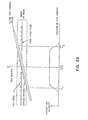
- Fig. 2 is an illustration of focus shift determination using a bias tilt between the test object surface and ideal image planes. Fig. 2A shows the test object surface in focus. Fig. 2B shows the test object surface out of focus.
- Fig. 3 shows an optical schematic of one apparatus embodying the present invention.
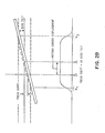
- Fig. 4 illustrates compound tilts about the x and y axes.
- Fig. 5 shows two scan measurement for shift and tilt determination.
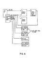
- Fig. 6 is a schematic of an electronic control system suitable for use in the present invention.
- The present invention provides an apparatus and process for precisely, repeatably and rapidly determining the optimum focus position for a lithographic tool. It is particularly suitable for use for photolithographic tools, such as, the Perkin-Elmer 500. In such a tool a 1:1 reflective imaging system images the mask onto a surface coated with a photosensitive material - typically a semiconductor wafer coated with photoresist. An annular region of best image quality is illuminated through a condenser system and sequentially exposed onto the surface through a synchronous scan of the mask and surface. Because of the small features (1 to 2 microns) being imaged with these tools, the depth of focus is also small (several microns) and accurate focus determination is essential. All current methods require a visual inspection step.
- In the present invention, the visual inspection is replaced with a machine-read inspection which is based upon a measurement of the light intensity diffracted from a fine line pattern which acts as a diffraction grating.
- A suitable mask pattern (1) is shown in Fig. 1. It consists of alternating bands of finely spaced horizontal and vertical lines. These lines are 1.5 microns wide and are located on 5 micron centers. In order to test the focussing in the lithographic tool a bias tilt is introduced. By tilting about the y axis, the vertical lines will be in focus over a limited extent in the x direction. This is illustrated sequentially in Fig. 2 where the lateral extent of the pattern is dependent on the tool depth of focus and the angle of tilt between the wafer and ideal image planes.
- After exposure in the photolithographic tool and subsequent development, the test surface (5) is illuminated, preferably using a laser (2), such as a helium-neon laser as shown in Fig. 3. The grating pattern on the surface diffracts light as shown in Fig. 3. No light is diffracted from the out of focus pattern. By translating the surface perpendicular to the grating lines, the extent of the exposed pattern can be determined by measuring the variations in diffraction efficiency. The extent of the in-focus pattern is determined by locating the transitions from out-of-focus to in-focus on each side of the pattern. The position of best focus is located at the center of the diffraction efficiency scan. By accurately determining this position with respect to the center of the surface, distance OC in Fig. 5, and knowing the bias tilt, α, for exposure, the amount of focus correction required,Af, can then be determined, by:
-

- In a preferred variation of the present invention, the detecting of the intensity of the diffracted beams is carried out with a broad area photodetector (6) which detects multiple plus and minus diffraction orders while excluding the zero order (7). This type of detector is illustrated in Fig. 3.
- Fig. 4 shows equal tilts about both the y and x axes. The shaded area represents the region on the surface that falls within the depth of focus. The y tilt has been intentionally introduced in order to make the measurement. When there is an additional tilt about the x axis, then the band of good focus no longer runs parallel to the y axis, but will be inclined at some angle, as shown in Fig. 4. Once again, by knowing the bias tilt value and measuring the band location, the amount of the x tilt can be determined. In order to make this measurement, two scans, displaced from each other by a predetermined distance,Λy, are necessary as shown in Fig. 5. The two scans are made and the x coordinates of the centers of the band are located at points A and B. The position C on the x-axis is then calculated and the distance OC is used to determine the amount of focus
shift using equation 1, while the angle that the line connecting points A & B makes with the y axis is related to the tilt,P, orthogonal to the bias tilt, by the following relationship: -

- This procedure can be repeated with the creation of a second test structure with the mask rotated by 90 degrees and the bias tilt introduced along the x axis. A second set of values for tilt and defocus will be obtained. We then have four values which can be used to provide the correct focusing and tilt correction for the lithography tool. Note that we have obtained two focus correction values. These correspond to the optimum focus locationfor horizontal and vertical lines. If the lithography tool has no astigmatism, these two locations should be equal. If not, then the difference between them is the astigmatism. This information can be used in an iterative manner to make optical alignment adjustments if desired.
- One additional concern in using this technique arises when the existing tilt in a tool is compound (i.e., it has both an x and a y tilt before the bias tilt is introduced). In this case, one must correct the bias tilt before calculating the defocus or orthogonal tilt. This is done by first performing all four scans. One then calculates intermediate tilt values based on the bias tilts used during exposure. When these intermediate tilt values are nonzero, one then calculates the actual tilt values using an iterative algorithm.
- Returning again to Fig. 3, a schematic of an apparatus useful in the present invention is provided. The helium-neon laser (2) used for illumination is unfocused. Two UDT silicon detectors are used. The scanning is done by McBain precision stages (3) driven by Compumotor Drivers (4).
- There is a shaft encoder attached to the x stage to generate position signals for data collection. The entire system is controlled and the data collected and processed using a computer, for example, an IBM PC.
- In carrying out the actual process of the present invention, an exposed silicon wafer with a photoresist surface relief structure is mounted on a vacuum chuck. There are two retractable pins built into the chuck for wafer registration. These pins locate the wafer in either of two orthogonal orientations to an accuracy of 0.05 mm. Thus, the wafer center is accurately positioned with respect to the reading beam and the wafer can be scanned in either the x or y direction. Since two scans are needed, a beam splitter and two detectors are used to provide these two scans in one physical translation of the stage. For reading the banding mask of Fig. 1 these beams are separated by 18 mm. The tool also has a perpendicular stage travel which is used to position the scans in the y direction, and may also be used for performing multiple scans at different y locations.
- The entire tool is typically built on a 2x2 foot optical breadboard. The associated power supplies and driving electronics may be housed in a 19x24x24 inch chassis rack.
- The electronic control system is shown schematically in Fig. 6. The X and Y compumotor stages are linked to an IBM PC through an RS-232 interface. The shaft encoder generates 100 trigger pulses/rev. as the stage is travelling. These pulses are used by a Tecmar Lab Tender Card to initiate A/D conversion of the photodetector data. After each encoder pulse is received, the data is converted and stored in separate arrays. The Tecmar card is also used to control the shutter electronics and wafer orientation switches.
- A suitable program may be written in Compiled Basic with some calls to machine code where speed is required. After the laser shutter is opened, the X stepping motor is started. In the interest of speed, the data is collected "on the fly" each time a pulse is received from the shaft encoder. At the end of the scan the laser shutter is closed; the motor is reversed and the stage is returned to a home position. The data is then plotted; a peak detection. algorithm is employed and the necessary calculations are performed to determine focus shift and the two orthogonal tilts. The results of the calculations are displayed on the PC display monitor and may optionally be printed on the on-line printer for hardcopy.
- The stage travels a distance of 4.0 inches and 4000 data points are taken at intervals of 0.001 inch. The lead screw has a pitch of 10/inch and the Compumotor driver produces 25,400 steps/rev. The data is gathered at a rate of 700 data points/sec with a maximum velocity of the stage of 7 rev/sec. The time required to scan and calculate for two wafers is less than one minute.
- When diffraction intensity is plotted versus position on the scanned wafer, the intensity goes from a minimum value through a broad maximum before returning to the background minimum. This corresponds to going from an out of focus condition, through the best focus, and then returning to the out of focus condition on the other side of the wafer. These conditions are produced by the bias tilt used during wafer exposure. In practice, the intensity of the diffracted light in the broad central region is lower than the intensity of the diffracted light near the edges of the surface relief pattern. These maxima enable us to detect the locations of the two outside peaks and more accurately determine the center position of the scan.
Claims (10)
characterized by
characterized by the steps of,
Applications Claiming Priority (2)
| Application Number | Priority Date | Filing Date | Title |
|---|---|---|---|
| US727644 | 1985-04-26 | ||
| US06/727,644 US4645338A (en) | 1985-04-26 | 1985-04-26 | Optical system for focus correction for a lithographic tool |
Publications (3)
| Publication Number | Publication Date |
|---|---|
| EP0199014A2 true EP0199014A2 (en) | 1986-10-29 |
| EP0199014A3 EP0199014A3 (en) | 1988-12-07 |
| EP0199014B1 EP0199014B1 (en) | 1993-05-26 |
Family
ID=24923439
Family Applications (1)
| Application Number | Title | Priority Date | Filing Date |
|---|---|---|---|
| EP86102278A Expired - Lifetime EP0199014B1 (en) | 1985-04-26 | 1986-02-21 | Apparatus and method for determining focus correction for a lithographic tool |
Country Status (4)
| Country | Link |
|---|---|
| US (1) | US4645338A (en) |
| EP (1) | EP0199014B1 (en) |
| JP (1) | JPS61250506A (en) |
| DE (1) | DE3688475D1 (en) |
Families Citing this family (10)
| Publication number | Priority date | Publication date | Assignee | Title |
|---|---|---|---|---|
| US5898479A (en) * | 1997-07-10 | 1999-04-27 | Vlsi Technology, Inc. | System for monitoring optical properties of photolithography equipment |
| US8032460B2 (en) * | 2000-07-27 | 2011-10-04 | Daita Frontier Fund, Llc | Authentication managing apparatus, and shop communication terminal |
| JP2002277967A (en) * | 2001-03-16 | 2002-09-25 | Fuji Photo Film Co Ltd | Focusing inspecting unit and focusing method |
| US7110099B2 (en) * | 2001-10-10 | 2006-09-19 | Accent Optical Technologies, Inc. | Determination of center of focus by cross-section analysis |
| US6885429B2 (en) * | 2002-06-28 | 2005-04-26 | Asml Holding N.V. | System and method for automated focus measuring of a lithography tool |
| US20060136717A1 (en) * | 2004-12-20 | 2006-06-22 | Mark Buer | System and method for authentication via a proximate device |
| US8295484B2 (en) * | 2004-12-21 | 2012-10-23 | Broadcom Corporation | System and method for securing data from a remote input device |
| JP2007317960A (en) * | 2006-05-26 | 2007-12-06 | Canon Inc | Method and apparadut for detecting exposure condition, and aligner |
| TWI383273B (en) | 2007-11-20 | 2013-01-21 | Asml Netherlands Bv | Method of measuring focus of a lithographic projection apparatus and method of calibrating a lithographic projection apparatus |
| US9798225B2 (en) | 2013-11-05 | 2017-10-24 | Asml Netherlands B.V. | Method of characterizing, method of forming a model, method of simulating, mask manufacturing method and device manufacturing method |
Citations (5)
| Publication number | Priority date | Publication date | Assignee | Title |
|---|---|---|---|---|
| US4153367A (en) * | 1976-05-19 | 1979-05-08 | Robert Bosch Gmbh | Method and devices for localizing flat chips on a carrier plate |
| US4327292A (en) * | 1980-05-13 | 1982-04-27 | Hughes Aircraft Company | Alignment process using serial detection of repetitively patterned alignment marks |
| US4420233A (en) * | 1981-05-25 | 1983-12-13 | Hitachi, Ltd. | Projecting apparatus |
| EP0111648A1 (en) * | 1982-12-21 | 1984-06-27 | The Perkin-Elmer Corporation | Alignment and focusing system for a scanning mask aligner |
| EP0115184A1 (en) * | 1982-12-28 | 1984-08-08 | Fujitsu Limited | An automatic focus control device |
Family Cites Families (9)
| Publication number | Priority date | Publication date | Assignee | Title |
|---|---|---|---|---|
| DE1447450A1 (en) * | 1963-06-14 | 1968-10-31 | Agfa Ag | Distance measuring or control device |
| US3945023A (en) * | 1974-03-29 | 1976-03-16 | Honeywell Inc. | Auto-focus camera with solid state range finder |
| US4201456A (en) * | 1976-04-22 | 1980-05-06 | Wolbarsht Myron L | Method and apparatus for detecting the focusing condition of an optical system |
| JPS5413330A (en) * | 1977-07-01 | 1979-01-31 | Olympus Optical Co Ltd | Automatic focus adjusting system |
| US4211489A (en) * | 1978-01-16 | 1980-07-08 | Rca Corporation | Photomask alignment system |
| JPS5576310A (en) * | 1978-12-05 | 1980-06-09 | Nippon Kogaku Kk <Nikon> | Automatic focusing device |
| JPS5897009A (en) * | 1981-12-04 | 1983-06-09 | Olympus Optical Co Ltd | Automatic focus adjusting method |
| US4583852A (en) * | 1983-03-31 | 1986-04-22 | The Perkin-Elmer Corporation | Attitude transfer system |
| US4585337A (en) * | 1985-01-14 | 1986-04-29 | Phillips Edward H | Step-and-repeat alignment and exposure system |
-
1985
- 1985-04-26 US US06/727,644 patent/US4645338A/en not_active Expired - Lifetime
-
1986
- 1986-01-29 JP JP61015981A patent/JPS61250506A/en active Granted
- 1986-02-21 DE DE8686102278T patent/DE3688475D1/en not_active Expired - Lifetime
- 1986-02-21 EP EP86102278A patent/EP0199014B1/en not_active Expired - Lifetime
Patent Citations (5)
| Publication number | Priority date | Publication date | Assignee | Title |
|---|---|---|---|---|
| US4153367A (en) * | 1976-05-19 | 1979-05-08 | Robert Bosch Gmbh | Method and devices for localizing flat chips on a carrier plate |
| US4327292A (en) * | 1980-05-13 | 1982-04-27 | Hughes Aircraft Company | Alignment process using serial detection of repetitively patterned alignment marks |
| US4420233A (en) * | 1981-05-25 | 1983-12-13 | Hitachi, Ltd. | Projecting apparatus |
| EP0111648A1 (en) * | 1982-12-21 | 1984-06-27 | The Perkin-Elmer Corporation | Alignment and focusing system for a scanning mask aligner |
| EP0115184A1 (en) * | 1982-12-28 | 1984-08-08 | Fujitsu Limited | An automatic focus control device |
Non-Patent Citations (2)
| Title |
|---|
| APPLIED OPTICS, vol. 23, no. 4, 15th February 1984, pages 628-632; G. MAKOSCH et al.: "Interferometric method for checking the mask alignment precision in the lithographic process" * |
| SPIE, vol. 174, 1979, pages 63-68; H.P. KLEINKNECHT: "Diffraction gratings as keys for automatic alignment in proximity and projection printing" * |
Also Published As
| Publication number | Publication date |
|---|---|
| EP0199014B1 (en) | 1993-05-26 |
| JPS61250506A (en) | 1986-11-07 |
| JPH0588835B2 (en) | 1993-12-24 |
| DE3688475D1 (en) | 1993-07-01 |
| US4645338A (en) | 1987-02-24 |
| EP0199014A3 (en) | 1988-12-07 |
Similar Documents
| Publication | Publication Date | Title |
|---|---|---|
| EP1413928B1 (en) | Apparatus and method for scanning exposure | |
| US4615621A (en) | Auto-focus alignment and measurement system and method | |
| US4748335A (en) | Method and aparatus for determining surface profiles | |
| US4707610A (en) | Method and apparatus for measuring surface profiles | |
| KR100266729B1 (en) | Surface position detecting method and scanning exposure method using the same | |
| EP0361933B1 (en) | Alignment system | |
| US5914774A (en) | Projection exposure apparatus with function to measure imaging characteristics of projection optical system | |
| EP0199014B1 (en) | Apparatus and method for determining focus correction for a lithographic tool | |
| US4580900A (en) | Auto focus alignment and measurement system and method | |
| US5446542A (en) | Mark position determining apparatus for use in exposure system | |
| Bruning et al. | An automated mask inspection system—AMIS | |
| EP0506039A2 (en) | Device and method for detecting position of edge of cutting tool | |
| EP0511847A2 (en) | Length-measuring device and exposure apparatus | |
| EP0198955A1 (en) | Apparatus for and a method of measuring the width of a line | |
| US4714331A (en) | Method and apparatus for automatic focusing | |
| US5475490A (en) | Method of measuring a leveling plane | |
| US7095904B2 (en) | Method and apparatus for determining best focus using dark-field imaging | |
| EP0338200B1 (en) | Method and apparatus for characterization of optical systems | |
| US4884890A (en) | Method for normalizing the detection signals of magnified images of fluorescing materials | |
| JP3255299B2 (en) | Position detection method and apparatus, and exposure method and apparatus | |
| EP0111635A2 (en) | Method of selecting the optimum focusing adjustment for an optical instrument | |
| EP0762216A2 (en) | Exposure method and apparatus and alignment evaluation method and apparatus | |
| US4601581A (en) | Method and apparatus of determining the true edge length of a body | |
| GB2172993A (en) | Automated optical linewidth measurement | |
| JP2000228345A (en) | Position detecting apparatus and method and exposing apparatus |
Legal Events
| Date | Code | Title | Description |
|---|---|---|---|
| PUAI | Public reference made under article 153(3) epc to a published international application that has entered the european phase |
Free format text: ORIGINAL CODE: 0009012 |
|
| AK | Designated contracting states |
Kind code of ref document: A2 Designated state(s): DE FR GB |
|
| 17P | Request for examination filed |
Effective date: 19870224 |
|
| PUAL | Search report despatched |
Free format text: ORIGINAL CODE: 0009013 |
|
| AK | Designated contracting states |
Kind code of ref document: A3 Designated state(s): DE FR GB |
|
| 17Q | First examination report despatched |
Effective date: 19910204 |
|
| GRAA | (expected) grant |
Free format text: ORIGINAL CODE: 0009210 |
|
| AK | Designated contracting states |
Kind code of ref document: B1 Designated state(s): DE FR GB |
|
| PG25 | Lapsed in a contracting state [announced via postgrant information from national office to epo] |
Ref country code: DE Effective date: 19930526 |
|
| REF | Corresponds to: |
Ref document number: 3688475 Country of ref document: DE Date of ref document: 19930701 |
|
| ET | Fr: translation filed | ||
| PG25 | Lapsed in a contracting state [announced via postgrant information from national office to epo] |
Ref country code: GB Effective date: 19940221 |
|
| PLBE | No opposition filed within time limit |
Free format text: ORIGINAL CODE: 0009261 |
|
| STAA | Information on the status of an ep patent application or granted ep patent |
Free format text: STATUS: NO OPPOSITION FILED WITHIN TIME LIMIT |
|
| 26N | No opposition filed | ||
| GBPC | Gb: european patent ceased through non-payment of renewal fee |
Effective date: 19940221 |
|
| PG25 | Lapsed in a contracting state [announced via postgrant information from national office to epo] |
Ref country code: FR Effective date: 19941031 |
|
| REG | Reference to a national code |
Ref country code: FR Ref legal event code: ST |