EP0197452B1 - Verfahren zur Herstellung von Epitaxieschichten mit hoher Qualität durch ein Molekularstrahlverfahren - Google Patents
Verfahren zur Herstellung von Epitaxieschichten mit hoher Qualität durch ein Molekularstrahlverfahren Download PDFInfo
- Publication number
- EP0197452B1 EP0197452B1 EP19860104239 EP86104239A EP0197452B1 EP 0197452 B1 EP0197452 B1 EP 0197452B1 EP 19860104239 EP19860104239 EP 19860104239 EP 86104239 A EP86104239 A EP 86104239A EP 0197452 B1 EP0197452 B1 EP 0197452B1
- Authority
- EP
- European Patent Office
- Prior art keywords
- substrate
- rough
- growth
- axis
- smooth
- Prior art date
- Legal status (The legal status is an assumption and is not a legal conclusion. Google has not performed a legal analysis and makes no representation as to the accuracy of the status listed.)
- Expired
Links
- 238000001451 molecular beam epitaxy Methods 0.000 title description 15
- 238000004519 manufacturing process Methods 0.000 title description 4
- 239000000758 substrate Substances 0.000 claims description 53
- 238000000034 method Methods 0.000 claims description 15
- JBRZTFJDHDCESZ-UHFFFAOYSA-N AsGa Chemical compound [As]#[Ga] JBRZTFJDHDCESZ-UHFFFAOYSA-N 0.000 claims description 7
- 229910001218 Gallium arsenide Inorganic materials 0.000 claims description 7
- 239000000463 material Substances 0.000 claims description 7
- 229910052733 gallium Inorganic materials 0.000 claims description 4
- GYHNNYVSQQEPJS-UHFFFAOYSA-N Gallium Chemical compound [Ga] GYHNNYVSQQEPJS-UHFFFAOYSA-N 0.000 claims description 3
- 230000004907 flux Effects 0.000 claims description 3
- 238000001228 spectrum Methods 0.000 description 9
- 230000007547 defect Effects 0.000 description 6
- 239000013078 crystal Substances 0.000 description 5
- 230000006872 improvement Effects 0.000 description 4
- 238000000103 photoluminescence spectrum Methods 0.000 description 4
- CSCPPACGZOOCGX-UHFFFAOYSA-N Acetone Chemical compound CC(C)=O CSCPPACGZOOCGX-UHFFFAOYSA-N 0.000 description 3
- KFZMGEQAYNKOFK-UHFFFAOYSA-N Isopropanol Chemical compound CC(C)O KFZMGEQAYNKOFK-UHFFFAOYSA-N 0.000 description 3
- YXFVVABEGXRONW-UHFFFAOYSA-N Toluene Chemical compound CC1=CC=CC=C1 YXFVVABEGXRONW-UHFFFAOYSA-N 0.000 description 3
- 239000000370 acceptor Substances 0.000 description 3
- 239000000203 mixture Substances 0.000 description 3
- 230000003287 optical effect Effects 0.000 description 3
- 239000012071 phase Substances 0.000 description 3
- IJGRMHOSHXDMSA-UHFFFAOYSA-N Atomic nitrogen Chemical compound N#N IJGRMHOSHXDMSA-UHFFFAOYSA-N 0.000 description 2
- 238000002441 X-ray diffraction Methods 0.000 description 2
- 230000015556 catabolic process Effects 0.000 description 2
- 238000006731 degradation reaction Methods 0.000 description 2
- 229910052738 indium Inorganic materials 0.000 description 2
- APFVFJFRJDLVQX-UHFFFAOYSA-N indium atom Chemical compound [In] APFVFJFRJDLVQX-UHFFFAOYSA-N 0.000 description 2
- 238000004943 liquid phase epitaxy Methods 0.000 description 2
- 238000011068 loading method Methods 0.000 description 2
- 238000005424 photoluminescence Methods 0.000 description 2
- 230000008569 process Effects 0.000 description 2
- 230000006798 recombination Effects 0.000 description 2
- 238000005215 recombination Methods 0.000 description 2
- 238000000859 sublimation Methods 0.000 description 2
- 230000008022 sublimation Effects 0.000 description 2
- 230000007704 transition Effects 0.000 description 2
- XLYOFNOQVPJJNP-UHFFFAOYSA-N water Substances O XLYOFNOQVPJJNP-UHFFFAOYSA-N 0.000 description 2
- 229910000980 Aluminium gallium arsenide Inorganic materials 0.000 description 1
- OKTJSMMVPCPJKN-UHFFFAOYSA-N Carbon Chemical compound [C] OKTJSMMVPCPJKN-UHFFFAOYSA-N 0.000 description 1
- ZOKXTWBITQBERF-UHFFFAOYSA-N Molybdenum Chemical compound [Mo] ZOKXTWBITQBERF-UHFFFAOYSA-N 0.000 description 1
- QAOWNCQODCNURD-UHFFFAOYSA-N Sulfuric acid Chemical compound OS(O)(=O)=O QAOWNCQODCNURD-UHFFFAOYSA-N 0.000 description 1
- RTAQQCXQSZGOHL-UHFFFAOYSA-N Titanium Chemical compound [Ti] RTAQQCXQSZGOHL-UHFFFAOYSA-N 0.000 description 1
- 230000004075 alteration Effects 0.000 description 1
- 238000004458 analytical method Methods 0.000 description 1
- XKRFYHLGVUSROY-UHFFFAOYSA-N argon Substances [Ar] XKRFYHLGVUSROY-UHFFFAOYSA-N 0.000 description 1
- 229910052786 argon Inorganic materials 0.000 description 1
- 238000000861 blow drying Methods 0.000 description 1
- 229910052799 carbon Inorganic materials 0.000 description 1
- 238000006243 chemical reaction Methods 0.000 description 1
- 238000004140 cleaning Methods 0.000 description 1
- 150000001875 compounds Chemical class 0.000 description 1
- 238000005520 cutting process Methods 0.000 description 1
- 239000002019 doping agent Substances 0.000 description 1
- 230000009977 dual effect Effects 0.000 description 1
- 230000000694 effects Effects 0.000 description 1
- 238000005530 etching Methods 0.000 description 1
- 230000005284 excitation Effects 0.000 description 1
- 239000001307 helium Substances 0.000 description 1
- 229910052734 helium Inorganic materials 0.000 description 1
- SWQJXJOGLNCZEY-UHFFFAOYSA-N helium atom Chemical compound [He] SWQJXJOGLNCZEY-UHFFFAOYSA-N 0.000 description 1
- 238000000097 high energy electron diffraction Methods 0.000 description 1
- 239000012535 impurity Substances 0.000 description 1
- 230000003993 interaction Effects 0.000 description 1
- 238000005259 measurement Methods 0.000 description 1
- 238000001000 micrograph Methods 0.000 description 1
- 230000004048 modification Effects 0.000 description 1
- 238000012986 modification Methods 0.000 description 1
- 229910052750 molybdenum Inorganic materials 0.000 description 1
- 239000011733 molybdenum Substances 0.000 description 1
- 230000000877 morphologic effect Effects 0.000 description 1
- 229910052757 nitrogen Inorganic materials 0.000 description 1
- 238000002360 preparation method Methods 0.000 description 1
- 239000004065 semiconductor Substances 0.000 description 1
- 229910052710 silicon Inorganic materials 0.000 description 1
- 239000010703 silicon Substances 0.000 description 1
- 235000011149 sulphuric acid Nutrition 0.000 description 1
- 230000003746 surface roughness Effects 0.000 description 1
- 229910052719 titanium Inorganic materials 0.000 description 1
- 239000010936 titanium Substances 0.000 description 1
Images


Classifications
-
- C—CHEMISTRY; METALLURGY
- C30—CRYSTAL GROWTH
- C30B—SINGLE-CRYSTAL GROWTH; UNIDIRECTIONAL SOLIDIFICATION OF EUTECTIC MATERIAL OR UNIDIRECTIONAL DEMIXING OF EUTECTOID MATERIAL; REFINING BY ZONE-MELTING OF MATERIAL; PRODUCTION OF A HOMOGENEOUS POLYCRYSTALLINE MATERIAL WITH DEFINED STRUCTURE; SINGLE CRYSTALS OR HOMOGENEOUS POLYCRYSTALLINE MATERIAL WITH DEFINED STRUCTURE; AFTER-TREATMENT OF SINGLE CRYSTALS OR A HOMOGENEOUS POLYCRYSTALLINE MATERIAL WITH DEFINED STRUCTURE; APPARATUS THEREFOR
- C30B23/00—Single-crystal growth by condensing evaporated or sublimed materials
- C30B23/02—Epitaxial-layer growth
-
- C—CHEMISTRY; METALLURGY
- C30—CRYSTAL GROWTH
- C30B—SINGLE-CRYSTAL GROWTH; UNIDIRECTIONAL SOLIDIFICATION OF EUTECTIC MATERIAL OR UNIDIRECTIONAL DEMIXING OF EUTECTOID MATERIAL; REFINING BY ZONE-MELTING OF MATERIAL; PRODUCTION OF A HOMOGENEOUS POLYCRYSTALLINE MATERIAL WITH DEFINED STRUCTURE; SINGLE CRYSTALS OR HOMOGENEOUS POLYCRYSTALLINE MATERIAL WITH DEFINED STRUCTURE; AFTER-TREATMENT OF SINGLE CRYSTALS OR A HOMOGENEOUS POLYCRYSTALLINE MATERIAL WITH DEFINED STRUCTURE; APPARATUS THEREFOR
- C30B29/00—Single crystals or homogeneous polycrystalline material with defined structure characterised by the material or by their shape
- C30B29/10—Inorganic compounds or compositions
- C30B29/40—AIIIBV compounds wherein A is B, Al, Ga, In or Tl and B is N, P, As, Sb or Bi
Definitions
- the present invention relates, in general, to a method for producing high quality epitaxial layers of group III-V, group II-VI and group IV compositions by means of molecular beam epitaxy (MBE). More particularly, the invention relates to a method of producing such epitaxial layers having smooth surface morphologies using MBE techniques under growth conditions which normally produce rough-surfaced growth.
- MBE molecular beam epitaxy
- Alterations in the MBE growth conditions have been suggested to alleviate the rough surface phenomenon. These include raising the substrate temperature, drastically reducing the growth rate and/or controlling the V/III flux ratio. However, in some situations it is desirable to grow Al x Ga 1-x As or other III-V layers under conditions which normally would produce rough surface morphologies. For instance, it may be desirable to grow such materials at commercially viable growth rates or at particular substrate temperatures. To date, there has been no method available to produce smooth-surfaced layers without altering the MBE growth conditions.
- a method of growing a substantially smooth surfaced epitaxial layer of monocrystalline material comprising the steps of: providing a monocrystalline gallium arsenide substrate having a growth surface oriented away from a ⁇ 100 ⁇ axis of said substrate toward a ⁇ 111 ⁇ gallium axis by between 2.75° and 10°; and exposing said substrate to molecular beam epitaxial growth conditions which normally would produce rough-surfaced growth on a nominally ⁇ 100 ⁇ substrate.
- a three chamber Varian GEN II MBE system was used to grow epitaxial layers of Al x Ga 1-x As on GaAs substrates.
- a closed-loop helium cryopump was connected to the growth chamber.
- the cleaning process applied to each substrate prior to loading into the MBE system comprised sequential rinsing in toluene, acetone, isopropyl alcohol and D.I. water; followed by etching in a 5:1:1 solution of H2SO4:H2O2:H2O; followed by a rinse in D.I. water and blow drying in dry nitrogen.
- each substrate was then mounted onto the molybdenum mounting blocks using molten indium.
- each substrate was out-gassed at a temperature of approximately 450° C for approximately 30 minutes in the analysis/preparation chamber of the system prior to loading into the growth chamber.
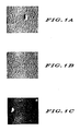
- FIGs. 1A - 1D are phase contrast photomicrographs illustrating the surface morphologies of four Al x Ga 1-x As layers grown by MBE on four different substrates (A,B,C,and D). The four samples illustrate the effect of mis-orienting the growth surface of the substrate by various amounts away from the normal orientation in a critical direction.
- the convention used in describing the orientation of a surface of a crystal substrate involves the relationship of a line perpendicular to the surface of the substrate to the axes of the substrate crystal.
- the axes of the crystal are defined with respect to the unit cell which specifies the atomic structure of the crystal.
- Sample A serves as a control and is nominally a ⁇ 100 ⁇ substrate, as is commonly used.
- the orientation of this substrate was determined by X-ray diffraction to be 0° 7' away from ⁇ 100 ⁇ toward a ⁇ 111 ⁇ A, or ⁇ 111 ⁇ gallium, axis.
- the orientation of sample B is 2° 33′ away from the ⁇ 100 ⁇ toward a ⁇ 111 ⁇ B axis.
- the orientation of sample C is 2° 45′ away from the ⁇ 100 ⁇ toward a ⁇ 111 ⁇ A axis.
- the orientation of sample D is 3° 6′ away from the ⁇ 100 ⁇ axis toward a ⁇ 111 ⁇ B axis.
- the growth conditions described normally produce rough surface morphology, as is evidenced in FIG. 1A.
- This surface morphology has been previously reported and has been cited as the cause of a number of performance degradations of devices constructed with such layers.
- Samples B and D (FIG.s 1B and 1D, respectively) also show surface roughness. It is apparent that a mis-orientation toward the ⁇ 111 ⁇ B axis is not effective to produce smooth-surfaced growth.
- phase contrast micrograph of sample C shows a surface substantially free of the rough morphology of the other samples.
- the only defect apparent in illustrated portion of sample C is an oval defect of the type which has been reported elsewhere and which is thought to be unrelated to rough surface morphology.
- FIG. 2 demonstrates that such a layer also exhibits an improved photoluminescence (PL) spectrum.
- the graph of FIG. 2 illustrates the PL spectra (at 4.2 K) of samples C and D. The spectra were obtained using the 5145 angstrom line of an argon ion laser as the excitation source. The intensity of the spectrum for sample D is expanded by a factor of three with respect to that of sample C.
- the peak in the spectrum of sample C which is labelled 1.698 eV is thought to result from the recombination of a bound exciton. This peak has a full width at half maximum of approximately 5 meV. This peak is thought to be indicative of relatively high quality material. A higher substrate temperature and/or a lower V/III flux ratio might have produced better results.
- the peak at 1.679 eV is thought to be related to a free-to-bound transition involving carbon acceptors.
- the peak at 1.664 eV is also thought to be acceptor-related, with the acceptor possibly being silicon. A phonon replica of this peak is seen at 1.629 eV.
- sample D shows a substantially lower quantity of bound exciton recombination than that of sample C. Indeed, no peak corresponding to an excitonic transition is apparent.
- the peak at 1.659 eV and its shoulder on the high energy side are believed to be related to impurities.
- the peak at 1.646 eV is believed to be defect-related. This spectrum is typical of those of all rough-surfaced samples.
- a comparison of the PL spectra of FIG. 2 demonstrates that the defect-related peak at 1.646 eV in sample D, which is typical of prior art layers, is greatly reduced in intensity in the critically mis-oriented sample C.
- the spectrum of sample C shows no evidence of a defect-related peak at the scale of FIG. 2.
- the bound exciton peak at 1.698 eV in the spectrum of sample C is thought to be evidence of improved material quality. This peak is apparently absent in the spectrum of sample D.
- the rough surface morphology of Al x Ga 1-x As layers grown by MBE on normally oriented substrates is believed to be related to the long range interaction between monatomic steps on the substrate surface. It is believed that the terraces, hillocks and other surface features are related to the reaction of the growing material to uneven surface energy caused by these steps. The bunching of material into hillocks, terraces and other features is thought to decrease the overall surface energy.
- a number of samples of A1 x Ga 1-x As were grown on GaAs substrates mis-oriented from the ⁇ 100 ⁇ toward the nearest ⁇ 111 ⁇ B axis by varying amounts.
- the substrate temperature was 675° C and the A1 fraction (x) was 0.15.
- These samples exhibited uniformly rough surface morphology and relatively poor photoluminescence spectra.
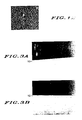
- FIG.s 3A and 3B are photomicrographs in cross-section illustrating the improvement in layer quality obtained by correctly mis-orienting the substrate.
- FIG. 3A is a cross-section at approximately 1000X of the layer grown on the nominally ⁇ 100> substrate in sample run 178 (see TABLE II).
- epitaxial layer 10 has a number of morphological defects visible at this magnification.
- FIG. 3B is a similar cross-sectional view of epitaxial layer 12 which was grown on the substrate oriented 5° from the ⁇ 100 ⁇ toward a ⁇ 111 ⁇ A axis in sample run 178.
- the improved surface morphology apparent in FIG. 1C corresponds to an improved structure throughout the layer. This implies that mis-orienting the substrate in the proper direction may improve the homogeneity of dopants introduced during layer growth.
- FIG.s 4A and 4B illustrate the improvement in surface morphology realized by the use of the present invention. Both are graphs representing the output of an instrument (a Sloan DEKTAK II profilometer) which scans the surface of a body and produces a representation of the surface profile thereof. In both FIG.s, the horizontal axis represents distance over the surface of the body in microns and the vertical axis represents the relative height of the surface in angstroms.
- a Sloan DEKTAK II profilometer a Sloan DEKTAK II profilometer
- FIG. 4A is the surface profile of a portion of the epitaxial layer grown on a nominally ⁇ 100 ⁇ substrate in sample run 153 (see TABLE III). The surface varies in relative height by more than 500 angstroms over distances of less than 10 microns.
- FIG. 4B is the surface profile of the layer grown on a substrate oriented 2.75° away from the ⁇ 100 ⁇ toward a ⁇ 111 ⁇ A axis.
- the vertical axis of this graph is expanded by approximately a factor of two with respect to that of FIG. 4A.
- This surface varies by less than approximately 100 angstroms over a distance of more than 10 microns.
- the layer of FIG. 4A is unacceptable.
- the layer grown on a critically mis-oriented substrate has sufficient surface smoothness to be useful in such an application.
Landscapes
- Chemical & Material Sciences (AREA)
- Engineering & Computer Science (AREA)
- Crystallography & Structural Chemistry (AREA)
- Materials Engineering (AREA)
- Metallurgy (AREA)
- Organic Chemistry (AREA)
- Inorganic Chemistry (AREA)
- Physical Deposition Of Substances That Are Components Of Semiconductor Devices (AREA)
Claims (5)
- Verfahren, das Wachstum einer epitaxialen Schicht aus einem monokristallinen Material mit einer praktisch glatten Oberfläche hervorzurufen,
bei dem eine Unterlage aus monokristallinem Galliumarsenid vorgesehen wird, deren Wachstumsfläche zwischen 2,75° und 10° aus der Achse 〈100〉 der Unterlage heraus in Richtung auf die Achse 〈111〉 des Galliums orientiert ist, und
bei dem die Unterlage den Bedingungen eines epitaxialen Wachstums durch einen Molekülstrahl ausgesetzt wird, welche normalerweise an einer nominellen 〈100〉-Unterlage ein Wachstum mit einer rauhen Oberfläche hervorrufen würden. - Verfahren gemäß Anspruch 1, bei dem zu dem Schritt, die Unterlage auszusetzen, ferner die Schritte gehören:
die Unterlage auf eine Temperatur zwischen 600° C und 700° C zu bringen und
die Unterlage einer Molekül-Strahlströmung aus Aluminium Al, Gallium Ga und Arsen As auszusetzen. - Verfahren gemäß Anspruch 2, bei dem die epitaxiale Schicht aus der Verbindung Al0,15Ga0,85As besteht und die Unterlage um mindestens 2,75° aus der 〈100〉-Achse heraus orientiert und auf einer Temperatur von annähernd 675° C gehalten wird.
- Verfahren gemäß Anspruch 2, bei dem die epitaxiale Schicht aus der Verbindung Al0,30Ga0,70As besteht und die Unterlage um mindestens 5° aus der 〈100〉-Achse heraus orientiert und auf einer Temperatur von annähernd 650° C gehalten wird.
- Verfahren gemäß Anspruch 2, bei dem die epitaxiale Schicht aus der Verbindung Al0,03Ga0,70As besteht und die Unterlage um mindestens 3° aus der 〈100〉-Achse heraus orientiert und auf einer Temperatur von annähernd 620° C gehalten wird.
Applications Claiming Priority (2)
| Application Number | Priority Date | Filing Date | Title |
|---|---|---|---|
| US72153785A | 1985-04-10 | 1985-04-10 | |
| US721537 | 1985-04-10 |
Publications (3)
| Publication Number | Publication Date |
|---|---|
| EP0197452A2 EP0197452A2 (de) | 1986-10-15 |
| EP0197452A3 EP0197452A3 (en) | 1988-08-17 |
| EP0197452B1 true EP0197452B1 (de) | 1992-05-13 |
Family
ID=24898369
Family Applications (1)
| Application Number | Title | Priority Date | Filing Date |
|---|---|---|---|
| EP19860104239 Expired EP0197452B1 (de) | 1985-04-10 | 1986-03-27 | Verfahren zur Herstellung von Epitaxieschichten mit hoher Qualität durch ein Molekularstrahlverfahren |
Country Status (4)
| Country | Link |
|---|---|
| EP (1) | EP0197452B1 (de) |
| JP (1) | JPH0770483B2 (de) |
| DE (1) | DE3685245D1 (de) |
| HK (1) | HK14095A (de) |
Families Citing this family (1)
| Publication number | Priority date | Publication date | Assignee | Title |
|---|---|---|---|---|
| JP4842667B2 (ja) * | 2006-02-23 | 2011-12-21 | ルネサスエレクトロニクス株式会社 | 成膜装置およびその調整方法 |
Family Cites Families (3)
| Publication number | Priority date | Publication date | Assignee | Title |
|---|---|---|---|---|
| JPS6026079B2 (ja) * | 1979-10-17 | 1985-06-21 | 松下電器産業株式会社 | 窒化ガリウムの成長方法 |
| US4419178A (en) * | 1981-06-19 | 1983-12-06 | Rode Daniel L | Continuous ribbon epitaxy |
| JPS59207896A (ja) * | 1983-05-09 | 1984-11-26 | Mitsubishi Monsanto Chem Co | 無機化合物単結晶薄膜の気相エピタキシヤル成長方法 |
-
1986
- 1986-03-27 DE DE8686104239T patent/DE3685245D1/de not_active Expired - Lifetime
- 1986-03-27 EP EP19860104239 patent/EP0197452B1/de not_active Expired
- 1986-04-10 JP JP61083216A patent/JPH0770483B2/ja not_active Expired - Lifetime
-
1995
- 1995-02-06 HK HK14095A patent/HK14095A/en not_active IP Right Cessation
Also Published As
| Publication number | Publication date |
|---|---|
| JPS621222A (ja) | 1987-01-07 |
| EP0197452A3 (en) | 1988-08-17 |
| DE3685245D1 (de) | 1992-06-17 |
| EP0197452A2 (de) | 1986-10-15 |
| JPH0770483B2 (ja) | 1995-07-31 |
| HK14095A (en) | 1995-02-10 |
Similar Documents
| Publication | Publication Date | Title |
|---|---|---|
| Irvine et al. | The growth by MOVPE and characterisation of CdxHg1− xTe | |
| Choopun et al. | Oxygen pressure-tuned epitaxy and optoelectronic properties of laser-deposited ZnO films on sapphire | |
| Olsen et al. | Crystal growth and properties of binary, ternary and quaternary (In, Ga)(As, P) alloys grown by the hydride vapor phase epitaxy technique | |
| USRE41310E1 (en) | Methods for growing semiconductors and devices thereof the alloy semiconductor gainnas | |
| US4960728A (en) | Homogenization anneal of II-VI compounds | |
| Ikeda et al. | MOCVD growth of AlGaInP at atmospheric pressure using triethylmetals and phosphine | |
| US12224172B2 (en) | Group III nitride substrate with oxygen gradient, method of making, and method of use | |
| Crumbaker et al. | Growth of InP on Si substrates by molecular beam epitaxy | |
| US4948751A (en) | Moelcular beam epitaxy for selective epitaxial growth of III - V compound semiconductor | |
| Cao et al. | Organometallic vapor-phase epitaxial growth of AlxGa1− xSb and AlxGa1− xAsySb1− y | |
| JP3399642B2 (ja) | 半導体発光素子層の形成方法 | |
| JP4100759B2 (ja) | 化合物半導体装置の製造方法 | |
| JPH01232732A (ja) | 半導体結晶製造方法 | |
| JP2004515919A (ja) | 正極性にドープされた広い禁止帯を有する半導体の製法 | |
| HK14095A (en) | Method for producing high quality epitaxial layers by molecular beam epitaxy | |
| US5384151A (en) | InGaAsP/GaAs diode laser | |
| Koljonen et al. | Growth of high-quality GaSb by metalorganic vapor phase epitaxy | |
| JPS5997595A (ja) | 液相エピタキシヤル成長方法 | |
| Dmitriev et al. | Removal of oxides from the surface (001) InP in ultra-high vacuum in an Arsenic flux | |
| US5441913A (en) | Process of making a semiconductor epitaxial substrate | |
| RU2366035C1 (ru) | Способ получения структуры многослойного фотоэлектрического преобразователя | |
| Feldman et al. | Very high mobility HgTe films grown on GaAs substrates by molecular‐beam epitaxy | |
| Pak et al. | A Study of Heteroepitaxy of InP on GaAs by Metalorganic Vapor‐Phase Epitaxy | |
| KR102936339B1 (ko) | 산화갈륨 박막 구조물, 이의 제조방법 및 이를 포함하는 포토다이오드 | |
| Lavrent'eva et al. | Low-temperature molecular-beam epitaxy of GaAs: effect of excess arsenic on the structure and properties of the GaAs layers |
Legal Events
| Date | Code | Title | Description |
|---|---|---|---|
| PUAI | Public reference made under article 153(3) epc to a published international application that has entered the european phase |
Free format text: ORIGINAL CODE: 0009012 |
|
| AK | Designated contracting states |
Kind code of ref document: A2 Designated state(s): DE FR GB IT NL |
|
| PUAL | Search report despatched |
Free format text: ORIGINAL CODE: 0009013 |
|
| AK | Designated contracting states |
Kind code of ref document: A3 Designated state(s): DE FR GB IT NL |
|
| 17P | Request for examination filed |
Effective date: 19890126 |
|
| 17Q | First examination report despatched |
Effective date: 19900222 |
|
| GRAA | (expected) grant |
Free format text: ORIGINAL CODE: 0009210 |
|
| AK | Designated contracting states |
Kind code of ref document: B1 Designated state(s): DE FR GB IT NL |
|
| REF | Corresponds to: |
Ref document number: 3685245 Country of ref document: DE Date of ref document: 19920617 |
|
| ITF | It: translation for a ep patent filed | ||
| ET | Fr: translation filed | ||
| PLBE | No opposition filed within time limit |
Free format text: ORIGINAL CODE: 0009261 |
|
| STAA | Information on the status of an ep patent application or granted ep patent |
Free format text: STATUS: NO OPPOSITION FILED WITHIN TIME LIMIT |
|
| 26N | No opposition filed | ||
| ITTA | It: last paid annual fee | ||
| PGFP | Annual fee paid to national office [announced via postgrant information from national office to epo] |
Ref country code: GB Payment date: 19971229 Year of fee payment: 13 |
|
| PGFP | Annual fee paid to national office [announced via postgrant information from national office to epo] |
Ref country code: FR Payment date: 19980116 Year of fee payment: 13 |
|
| PGFP | Annual fee paid to national office [announced via postgrant information from national office to epo] |
Ref country code: DE Payment date: 19980120 Year of fee payment: 13 |
|
| PGFP | Annual fee paid to national office [announced via postgrant information from national office to epo] |
Ref country code: NL Payment date: 19980313 Year of fee payment: 13 |
|
| PG25 | Lapsed in a contracting state [announced via postgrant information from national office to epo] |
Ref country code: GB Free format text: LAPSE BECAUSE OF NON-PAYMENT OF DUE FEES Effective date: 19990327 |
|
| PG25 | Lapsed in a contracting state [announced via postgrant information from national office to epo] |
Ref country code: NL Free format text: LAPSE BECAUSE OF NON-PAYMENT OF DUE FEES Effective date: 19991001 |
|
| GBPC | Gb: european patent ceased through non-payment of renewal fee |
Effective date: 19990327 |
|
| PG25 | Lapsed in a contracting state [announced via postgrant information from national office to epo] |
Ref country code: FR Free format text: LAPSE BECAUSE OF NON-PAYMENT OF DUE FEES Effective date: 19991130 |
|
| NLV4 | Nl: lapsed or anulled due to non-payment of the annual fee |
Effective date: 19991001 |
|
| REG | Reference to a national code |
Ref country code: FR Ref legal event code: ST |
|
| PG25 | Lapsed in a contracting state [announced via postgrant information from national office to epo] |
Ref country code: DE Free format text: LAPSE BECAUSE OF NON-PAYMENT OF DUE FEES Effective date: 20000101 |
|
| PG25 | Lapsed in a contracting state [announced via postgrant information from national office to epo] |
Ref country code: IT Free format text: LAPSE BECAUSE OF NON-PAYMENT OF DUE FEES;WARNING: LAPSES OF ITALIAN PATENTS WITH EFFECTIVE DATE BEFORE 2007 MAY HAVE OCCURRED AT ANY TIME BEFORE 2007. THE CORRECT EFFECTIVE DATE MAY BE DIFFERENT FROM THE ONE RECORDED. Effective date: 20050327 |