EP0197424A2 - Process of fabricating a heterojunction bipolar transistor - Google Patents
Process of fabricating a heterojunction bipolar transistor Download PDFInfo
- Publication number
- EP0197424A2 EP0197424A2 EP86104067A EP86104067A EP0197424A2 EP 0197424 A2 EP0197424 A2 EP 0197424A2 EP 86104067 A EP86104067 A EP 86104067A EP 86104067 A EP86104067 A EP 86104067A EP 0197424 A2 EP0197424 A2 EP 0197424A2
- Authority
- EP
- European Patent Office
- Prior art keywords
- layer
- regions
- region
- semiconductor material
- doped
- Prior art date
- Legal status (The legal status is an assumption and is not a legal conclusion. Google has not performed a legal analysis and makes no representation as to the accuracy of the status listed.)
- Granted
Links
- 238000000034 method Methods 0.000 title claims description 47
- 230000008569 process Effects 0.000 title claims description 42
- 239000004065 semiconductor Substances 0.000 claims abstract description 77
- 239000000463 material Substances 0.000 claims abstract description 60
- 229910052732 germanium Inorganic materials 0.000 claims description 106
- GNPVGFCGXDBREM-UHFFFAOYSA-N germanium atom Chemical compound [Ge] GNPVGFCGXDBREM-UHFFFAOYSA-N 0.000 claims description 105
- JBRZTFJDHDCESZ-UHFFFAOYSA-N AsGa Chemical compound [As]#[Ga] JBRZTFJDHDCESZ-UHFFFAOYSA-N 0.000 claims description 93
- 229910001218 Gallium arsenide Inorganic materials 0.000 claims description 93
- 239000002019 doping agent Substances 0.000 claims description 25
- 229910052710 silicon Inorganic materials 0.000 claims description 18
- 239000010703 silicon Substances 0.000 claims description 18
- HZXMRANICFIONG-UHFFFAOYSA-N gallium phosphide Chemical compound [Ga]#P HZXMRANICFIONG-UHFFFAOYSA-N 0.000 claims description 11
- 229910005540 GaP Inorganic materials 0.000 claims description 10
- 238000010438 heat treatment Methods 0.000 claims description 5
- 238000005530 etching Methods 0.000 claims 1
- ZOXJGFHDIHLPTG-UHFFFAOYSA-N Boron Chemical compound [B] ZOXJGFHDIHLPTG-UHFFFAOYSA-N 0.000 description 35
- 229910052796 boron Inorganic materials 0.000 description 35
- 229920002120 photoresistant polymer Polymers 0.000 description 23
- 238000002513 implantation Methods 0.000 description 18
- 238000005468 ion implantation Methods 0.000 description 16
- XUIMIQQOPSSXEZ-UHFFFAOYSA-N Silicon Chemical compound [Si] XUIMIQQOPSSXEZ-UHFFFAOYSA-N 0.000 description 14
- 239000011248 coating agent Substances 0.000 description 13
- 238000000576 coating method Methods 0.000 description 13
- 238000000137 annealing Methods 0.000 description 8
- 239000000758 substrate Substances 0.000 description 7
- 239000007943 implant Substances 0.000 description 5
- 238000004519 manufacturing process Methods 0.000 description 5
- 238000001451 molecular beam epitaxy Methods 0.000 description 5
- 230000009467 reduction Effects 0.000 description 5
- 230000004888 barrier function Effects 0.000 description 4
- 230000015572 biosynthetic process Effects 0.000 description 4
- 230000005669 field effect Effects 0.000 description 4
- 229910000927 Ge alloy Inorganic materials 0.000 description 3
- BYDQGSVXQDOSJJ-UHFFFAOYSA-N [Ge].[Au] Chemical compound [Ge].[Au] BYDQGSVXQDOSJJ-UHFFFAOYSA-N 0.000 description 3
- 238000001465 metallisation Methods 0.000 description 3
- 230000004048 modification Effects 0.000 description 3
- 238000012986 modification Methods 0.000 description 3
- 230000003071 parasitic effect Effects 0.000 description 3
- 238000002360 preparation method Methods 0.000 description 3
- 230000000694 effects Effects 0.000 description 2
- 230000006872 improvement Effects 0.000 description 2
- 238000002347 injection Methods 0.000 description 2
- 239000007924 injection Substances 0.000 description 2
- 230000010354 integration Effects 0.000 description 2
- 150000002500 ions Chemical class 0.000 description 2
- 238000002955 isolation Methods 0.000 description 2
- 238000005086 pumping Methods 0.000 description 2
- 230000006798 recombination Effects 0.000 description 2
- 238000005215 recombination Methods 0.000 description 2
- VYZAMTAEIAYCRO-UHFFFAOYSA-N Chromium Chemical compound [Cr] VYZAMTAEIAYCRO-UHFFFAOYSA-N 0.000 description 1
- 241001101998 Galium Species 0.000 description 1
- OAICVXFJPJFONN-UHFFFAOYSA-N Phosphorus Chemical compound [P] OAICVXFJPJFONN-UHFFFAOYSA-N 0.000 description 1
- 230000003213 activating effect Effects 0.000 description 1
- 230000003321 amplification Effects 0.000 description 1
- 239000000969 carrier Substances 0.000 description 1
- 229910052804 chromium Inorganic materials 0.000 description 1
- 239000011651 chromium Substances 0.000 description 1
- 238000010276 construction Methods 0.000 description 1
- 230000001627 detrimental effect Effects 0.000 description 1
- 238000003199 nucleic acid amplification method Methods 0.000 description 1
- 230000035515 penetration Effects 0.000 description 1
- 229910052698 phosphorus Inorganic materials 0.000 description 1
- 239000011574 phosphorus Substances 0.000 description 1
- 238000012827 research and development Methods 0.000 description 1
- 230000007480 spreading Effects 0.000 description 1
- 238000003892 spreading Methods 0.000 description 1
- 239000000126 substance Substances 0.000 description 1
- 238000006467 substitution reaction Methods 0.000 description 1
Images


Classifications
-
- H—ELECTRICITY
- H01—ELECTRIC ELEMENTS
- H01L—SEMICONDUCTOR DEVICES NOT COVERED BY CLASS H10
- H01L29/00—Semiconductor devices adapted for rectifying, amplifying, oscillating or switching, or capacitors or resistors with at least one potential-jump barrier or surface barrier, e.g. PN junction depletion layer or carrier concentration layer; Details of semiconductor bodies or of electrodes thereof ; Multistep manufacturing processes therefor
- H01L29/02—Semiconductor bodies ; Multistep manufacturing processes therefor
- H01L29/12—Semiconductor bodies ; Multistep manufacturing processes therefor characterised by the materials of which they are formed
- H01L29/26—Semiconductor bodies ; Multistep manufacturing processes therefor characterised by the materials of which they are formed including, apart from doping materials or other impurities, elements provided for in two or more of the groups H01L29/16, H01L29/18, H01L29/20, H01L29/22, H01L29/24, e.g. alloys
- H01L29/267—Semiconductor bodies ; Multistep manufacturing processes therefor characterised by the materials of which they are formed including, apart from doping materials or other impurities, elements provided for in two or more of the groups H01L29/16, H01L29/18, H01L29/20, H01L29/22, H01L29/24, e.g. alloys in different semiconductor regions, e.g. heterojunctions
-
- H—ELECTRICITY
- H01—ELECTRIC ELEMENTS
- H01L—SEMICONDUCTOR DEVICES NOT COVERED BY CLASS H10
- H01L29/00—Semiconductor devices adapted for rectifying, amplifying, oscillating or switching, or capacitors or resistors with at least one potential-jump barrier or surface barrier, e.g. PN junction depletion layer or carrier concentration layer; Details of semiconductor bodies or of electrodes thereof ; Multistep manufacturing processes therefor
- H01L29/40—Electrodes ; Multistep manufacturing processes therefor
- H01L29/41—Electrodes ; Multistep manufacturing processes therefor characterised by their shape, relative sizes or dispositions
- H01L29/423—Electrodes ; Multistep manufacturing processes therefor characterised by their shape, relative sizes or dispositions not carrying the current to be rectified, amplified or switched
- H01L29/42304—Base electrodes for bipolar transistors
-
- H—ELECTRICITY
- H01—ELECTRIC ELEMENTS
- H01L—SEMICONDUCTOR DEVICES NOT COVERED BY CLASS H10
- H01L29/00—Semiconductor devices adapted for rectifying, amplifying, oscillating or switching, or capacitors or resistors with at least one potential-jump barrier or surface barrier, e.g. PN junction depletion layer or carrier concentration layer; Details of semiconductor bodies or of electrodes thereof ; Multistep manufacturing processes therefor
- H01L29/66—Types of semiconductor device ; Multistep manufacturing processes therefor
- H01L29/68—Types of semiconductor device ; Multistep manufacturing processes therefor controllable by only the electric current supplied, or only the electric potential applied, to an electrode which does not carry the current to be rectified, amplified or switched
- H01L29/70—Bipolar devices
- H01L29/72—Transistor-type devices, i.e. able to continuously respond to applied control signals
- H01L29/73—Bipolar junction transistors
- H01L29/737—Hetero-junction transistors
- H01L29/7371—Vertical transistors
Definitions
- the present invention relates to semiconductor devices and, more particularly, to a heterojunction bipolar transistor device.
- the present invention further relates to a process of fabricating a semiconductor device, particularly, a heterojunction bipolar transistor device or a unit circuit such as an emitter-coupled logic composed of heterojunction bipolar transistors.
- MOS metal-oxide-semiconductor
- Typical of homogeneous pn junction devices are bipolar transistors. Bipolar transistors are contrasted by unipolar or field-effect transistors which may be of any of the homogeneous pn junction, Schottky barrier and metal-oxide-semiconductor configurations.
- the high-frequency performance of a unipolar transistors can be improved by microminiaturization of the' gate of the device while that of a bipolar transistor improved by reducing the thickness of the base region of the device.
- the devices be designed and fabricated with a view to reducing the parasitic resistances and capacitances to be involved in the devices.
- it is of particular significance to reduce the source/gate and drain/gate resistances for transistors of the unipolar type and the base resistances and the emitter/base capacitances for bipolar transistors.
- bipolar transistors In a semiconductor integrated circuit composed of a number of transistors provided as component devices, unipolar transistors excel bipolar transistors for their smaller power dissipation rates but are inferior to the latter for their capabilities to drive loads. Where load driving capabilities are among preferential requirements of component devices forming a semiconductor integrated circuit, bipolar transistors are used almost exclusively over unipolar devices. Bipolar transistors are generally fabricated of silicon and provide high-frequency performances having limitations represented by cutoff frequencies of from It giga hertz to 20 giga hertz as well known in the art.
- a prime object of the present invention is to provide a bipolar transistor with an increased cutoff frequency and more adaptability to integration and a process of fabricating such a transistor.
- a bipolar transistor comprising a) a first layer of a first semiconductor material having a first conductivity type, b) a second layer on the first layer,'the second layer being of a second semiconductor material having a second conductivity type opposite to the first conductivity type, the second semiconductor material having an energy bandgap less than that of the first semiconductor material, c) a third layer on the second layer, the third layer being of the second semiconductor material and having the first conductivity type, d) a first doped region in the first layer, the first doped region being of the first semiconductor material and being doped to be semi-insulating regions, and e) a second doped region in the third layer, the second doped region being of the second semiconductor material and being doped to the second conductivity type, f) the second layer having a portion forming an active base region, the third layer having a portion forming a collector region in contact with the active base region, the first doped region defining in the first layer an active emitter region in
- a process of fabricating a bipolar transistor comprising the steps of a) epitaxially forming a first layer of a first semiconductor material having a first conductivity type, b) epitaxially forming on the first layer a second layer of a second semiconductor material having a second conductivity type opposite to the first conductivity type, the second layer having a portion for forming an active base region, the second semiconductor material having an energy bandgap less than that of the first semiconductor material, c) epitaxially forming on the second layer a third layer of the second semiconductor material and having the first conductivity type, the third layer having a portion for forming a collector region in contact with the active base region, and d) introducing a dopant of the second conductivity type into a portion of the third layer and through the second layer into a portion of the first layer, e) heating the resultant structure for converting the doped portion of the first layer into a semi-insulating region and converting the do
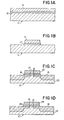
- the shown example of a process according to the present invention starts with preparation of an n-type epilayer 10 of GaAs (hereinafter referred to as GaAs). On this n-type GaAs epilayer 10 is grown a p-type monocrystalline germanium epilayer 12 by, for example, molecular beam epitaxy (M BE ), whereupon an n-type monocrystalline germanium epilayer 14 is grown on the p-type germanium epilayer 12 also by molecular beam epitaxy.
- M BE molecular beam epitaxy
- 1A shows the semiconductor structure thus obtained, wherein a heterojunction is formed between the n-type GaAs epilayer 10 which is to result, in part, in an emitter region and the p-type germanium epilayer 12 which is to result, in part, in an active base region as the process advances.
- a photoresist is spun on to the surface of the upper n-type germanium epilayer 14 and the resultant photoresist coating is patterned and etched to define a desired device region of the transistor device to be fabricated.
- the upper two germanium epilayers 12 and 14 are then etched away with the remaining photoresist coating used as a mask to leave the epilayers 12 and 14 in mesa form as illustrated in Fig. 1B.
- a central portion of the upper n-type germanium epilayer 14 of the land thus formed on the n-type GaAs epilayer 10 is covered with a mask (not shown) defining a collector region of the transistor device to be fabricated.
- a p-type dopant such as boron is injected by ion implantation into the unmasked areas of the epilayers 12 and 14 and the exposed area of the n-type GaAs epilayer 10 surrounding the land of the germanium epilayers 12 and 14 and further into an upper surface portion of the area of the GaAs epilayer 10 which underlies the p-type germanium epilayer 12.
- the energy to be used for the ion implantation is selected to assure the p-type dopant to reach into the upper surface portion of the area of the GaAs epilayer 10 underlying the p-type germanium epilayer 12.
- the n-type GaAs epilayer 10 has a doped surface region 16
- the lower p-type germanium epilayer 12 has a doped region 18
- the upper n-type germanium epilayer 14 has a doped region 20, in addition to an original unimplanted lower layer region 22 underlying the doped surface region 16 of the GaAs epilayer 10, as shown in Fig. 1C.
- the resultant semiconductor structure is annealed at a temperature within the range of from 400°C to 600°C so that the atoms of boron injected into each of the regions 18 and 20 are thermally activated.
- the doped region 20 of the upper n-type germanium epilayer 14 is thus converted into a p-type germanium region 24, and the doped region 18 of the lower p-type-germanium epilayer 14 becomes a heavily doped p-type germanium region 26, as shown in Fig. 1D.
- These coextensive or aligned p-type germanium regions 24 and 26 are to form in combination a base contact or connecting portion of the transistor device to be fabricated.
- the surface region 16 doped with boron of the n-type GaAs epilayer 10 becomes semi-insulating as a result of the injection of the dopant due to the implant damage caused therein.
- the semi-insulating GaAs region 16 remain as such after the annealing process because the annealing temperature lower than 600°C is short of activating the atoms of boron injected into the region 16 of the n-type GaAs epilayer 10 and because the implant damage as caused by the implantation of boron into the GaAs epilayer 10 remains unrelieved by the annealing process.
- a collector region is defined by the region surrounded by the doped p-type germanium region 24 of the initial n-type germanium epilayer 14, and an active base region is defined by the region surrounded by the heavily doped p-type germanium region 26 of the initial p-type germanium epilayer 12 which is. That portion of the region 22 of the initial n-type GaAs epilayer 10 which directly underlies this active base region and which is surrounded by the semi-insulating surface region 16 of the GaAs epilayer 10 defines the effective width of the emitter region, as will be seen from Fig. 1D.
- the effective width of the emitter region is thus dictated by the boundary of the semi-insulating surface region 16 of GaAs contiguous with the emitter region directly underlying the active base region 12 of p-type germanium.
- An n-p-n heterojunction bipolar transistor (HBT) is completed with a collector electrode layer 28 formed on the collector region 14, a base electrode layer 30 formed on the base contact or connecting portion provided by the aligned p-type germanium regions 24 and 26, and an emitter electrode layer 32 formed on the reverse surface of the n-type GaAs epilayer 10 as shown in Fig. lE.
- These electrode layers may be formed by a metalization process with, for example, a gold-germanium alloy.
- the bipolar transistor has a heterogeneous emitter-base junction interface between the n-type GaAs epilayer 10 and the p-type germanium region 12.
- the" bandgap of the emitter, region 22 of the n-type GaAs epilayer 10 is wider than that of the p-type germanium epilayer 12 forming the active base region so that the edges of the conduction and valence bands of the two layers have discontinuities at the heterojunction interface between the layers.
- the discontinuity in the energy level at the band edge of the conduction band results in an initial velocity of movement of the electrons to be transported from the emitter region 14 into the active base region -12 of the transistor. This initial velocity reduces the period of time for which the electrons travel through the overall base region and thus contributes to improvement of the high-frequency performance of the device.
- the discontinuity in the energy level at the band edge of the valence band results in creation of a barrier to the movement of holes which attempt to enter the emitter region 14 from the active base region 12 and contributes to reduction in the recombination of holes and electrons within the emitter region 14, thereby providing an increased electron pumping efficiency across the heterojunction interface between the layers 12 and 14.
- the atoms of boron injected into the defined region of the initial n-type germanium epilayer 14 convert the doped region 20 of the epilayer 14 into the p-type germanium region 24 and the atoms of boron injected into the defined region the initial p-type germanium epilayer 12 convert the doped region 18 of the epilayer 12 into the p +-type germanium region 26.
- the atoms of boron injected into the initial n-type GaAs epilayer 10 render the doped surface region 16 semi-insulating and are thus conducive to reducing the effective area of the base-emitter junction and the base spreading resistance of the device, viz., the resistance through the extrinsic, viz., contact or connecting base portion formed by the aligned p-type germanium regions 26 and 24.
- the combination of these effects result in significant reduction in the capacitance of the base-emitter junction and accordingly permits achievement of faster operation in the device.
- the bipolar transistor device fabricated as hereinbefore described is further advantageous in that the active emitter region is aligned with the collector region across the active base region and is thus substantially coextensive with the collector region due to the formation of the boron-implanted semi-insulating region around the active emitter region.
- a bipolar transistor when used in the form of grounded-emitter connection, produces a limited emitter inductance which would otherwise impair the high-frequency performance characteristics of the device.
- a bipolar transistor according to the present invention may have an emitter electrode layer or two or more emitter electrode regions provided on the upper surface of the device structure. For this purpose, the fabrication process step resulting in the structure shown in Fig.
- 1B may be followed by formation of a mask patterned to cover not only the central portion of the upper n-type germanium epilayer 14 as described but also at least one portion of the n-type GaAs epilayer 10 within the area in which the transistor device is to be fabricated.
- a p-type dopant such as boron is then injected by ion implantation into the unmasked areas of the p-type and n-type germanium epilayers 12 and 14, the upper surface portion of that area of the GaAs epilayer 10 which underlies the p-type germanium epilayer 12, and the exposed area of the GaAs epilayer 10 as shown in Fig. 2A.
- the n-type GaAs epilayer 10 has an undoped region 22' partly exposed at the upper surface of the epilayer 10 as well as the doped surface region 16 of GaAs in part underlying the doped germanium regions 18 and 20 and in part exposed at the upper surface of the epilayer 10.
- the resultant structure is annealed as discussed previously so that the atoms of the p-type dopant injected into each of the regions 18 and 20 are activated to form the p-type germanium region 24 and the heavily doped p-type germanium region 26, respectively, as shown in Fig. 2B.
- An n-p-n bipolar transistor is thus obtained with a collector electrode layer 28 formed on the collector region 14, a base electrode layer region 30 formed on the active base region 12 and an emitter electrode layer region 32' formed on the upper surface of the n-type GaAs epilayer 10.
- Figs. 3A to 3E starts with preparation of a monocrystalline GaAs substrate 34 doped with, for example, chromium to be semi-insulating.
- An epilayer is grown on this semi-insulating GaAs substrate 34 and doped with, for example, silicon to a carrier concentration of 1x10 18 atoms/cm -3 to form an n-type GaAs epilayer 10.
- On this n-type GaAs epilayer 10 is grown a monocrystalline germanium epilayer 12 to a thickness of 0.1 micron by molecular beam epitaxy and is doped with, for example, boron to a carrier concentration of 1x10 17 atoms/cm -3 .
- a monocrystalline germanium epilayer 14 is grown on the p-type germanium epilayer 12 to a thickness of 0.6 micron also by molecular beam epitaxy and is doped with, for example, phosphorus to a carrier concentration of 1x10 16 atoms/cm -3 .
- Fig. 3A shows the semiconductor structure thus obtained.
- a heterojunction is formed between the n-type GaAs epilayer 10 which is to result, in part, in two collector regions and the p-type germanium epilayer 12 which is to result, in part, in two active base regions as the process advances.
- a photoresist is then spun on to the surface of the upper n-type germanium epilayer 14 to form a photoresist coating (not shown).
- the photoresist coating is patterned and etched to define two collector regions on both sides of a common emitter region of the emitter-coupled logic to be fabricated.
- a p-type dopant such as boron is injected by ion implantation into the unmasked areas of the epilayers 12 and 14 and far into surface portions of the n-type GaAs epilayer 10 underlying the unmasked areas of the germanium epilayers 12 and 14.
- the energy to be used for the ion implantation is selected to assure the p-type dopant to penetrate into the upper surface portions of the GaAs epilayer 10 underlying the germanium epilayers 12 and 14.
- the n-type GaAs epilayer 10 has three doped surface regions 16, 16' and 16"
- the lower p-type germanium epilayer 12 has three doped regions 18, 18' and 18
- the upper n-type germanium epilayer 14 has three doped regions 20, 20' and 20" in addition to an original unimplanted lower layer region 22 of the GaAs epilayer 10, as shown in Fig. 3B.
- the doped surface regions 16, 16' and 16" of the n-type GaAs epilayer 10 are separated from one another across portions 36 and 36' of the unimplanted lower layer region 22 of the epilayer 10.
- the doped regions 18, 18' and 18" of the lower p-type germanium epilayer 12 overlie the doped surface regions 16, 16' and 16", respectively, of the GaAs epilayer 10 and are separated from one another across unimplanted regions 38 and 38' of the germanium epilayer 12.
- the doped regions 20, 20' and 20" of the upper n-type p-type germanium epilayer 14 overlie the doped regions 18, 18' and 18", respectively, of the lower p-type germanium epilayer 12 and are separated from one another across unimplanted regions 40 and 40' of the germanium epilayer 14.
- the unimplanted region 22 of the n-type GaAs epilayer 10 is to result in the common emitter region, and the unimplanted regions 38 and 38' of the p-type germanium epilayer 12 are to result in the active base regions, respectively, of the emitter-coupled logic circuit.
- the unimplanted regions 40 and 40' of the n-type germanium epilayer 14 are to result in the collector regions, respectively, of the emitter-coupled logic circuit.
- Implantation-of boron far into the n-type GaAs epilayer 10 to form the doped surface regions 16, 16' and 16" in the epilayer 10 as discussed above is of particular importance since the geometries, viz., the width and length of the common emitter region to be formed are dictated by the geometries, viz., the width and length of the two collector regions to result from the unimplanted regions 40 and 40', respectively, of the n-type germanium epilayer 14.
- the resultant semiconductor structure is annealed at a temperature within the range of from 400°C to 600°C so that the atoms of boron injected into the regions 18, 18' and 18" of the initial p-type germanium epilayer 12 and the regions 20, 20' and 20" of the initial n-type germanium epilayer 14 are thermally activated.
- the doped regions 20, 20' and 20" of the initial n-type germanium epilayer 14 are thus converted into p-type germanium regions 24, 24' and 24", respectively, and the doped regions 18, 18' and 18" of the initial p-type germanium epilayer 14 become heavily doped p-type germanium regions 26, 26' and 26", respectively, as shown in Fig. 3C.
- the aligned p-type regions 24 and 26 form in combination a base contact or connecting region 42 of one of the transistors to form the emitter-coupled logic and, likewise, the aligned p-type regions 24' and 26' form in combination a base contact or connecting region 42' 'of the other transistor of the emitter-coupled logic.
- the regions 16, 16' and 16" doped with boron of the n-type GaAs epilayer 10 are rendered semi-insulating by the injection of the dopant due to the implant damage caused therein.
- these semi-insulating GaAs regions remain as such after the annealing process because the atoms of boron injected into these regions can not be activated by the annealing at a temperature lower than 600°C and because the implant damage as caused by the implantation of boron into the GaAs epilayer 10 remains unrelieved by the annealing process, as previously noted.
- These semi-insulating GaAs regions 16, 16' and 16" separate the base contact or connecting regions 42 and 42' from the unimplanted emitter-forming region 22 of the n-type GaAs epilayer 10.
- a photoresist is then spun on to the surface of the resultant structure to form a photoresist coating (not shown) on the surface of the toplevel layer forming the regions 24, 24' and 24" and regions 42 and 42'.
- the photoresist coating is patterned and etched to define a desired emitter electrode region through the region 24" between the collector-forming regions 40 and 40' of the toplevel layer.
- the remaining photoresist coating is used as a mask to etch the toplevel layer for forming a trench 44 extending through the aligned p-type germanium regions 24" and 26" and the semi-insulating GaAs region 16" to reach the surface of the unimplanted emitter-forming region 22 of the initial n-type GaAs epilayer 10 as shown in Fig.
- the trench 44 thus formed has its bottom surrounded by a remaining filament of the semi-insulating GaAs region' 16" so that the width of the emitter region to be formed below the trench 44 might not be reduced as a result of the formation of the trench 44.
- a pair of n-p-n heterojunction bipolar transistors are thus completed by a metalization process with, for example, a gold-germanium alloy.
- collector electrode regions 28 and 28' are formed on the unimplanted regions 40 and 40' of the initial n-type germanium layer 14 and base electrode regions 30 and 30' are formed on the p-type germanium regions 24 and 24' forming part of the base contact or connecting portions of the device.
- An emitter electrode layer 32 is formed on the exposed surface of the unimplanted region 22 of the initial n-type GaAs epilayer 10 below the trench as shown in Fig. 3E.
- These two bipolar transistors form an emitter-coupled logic circuit having the collector regions 40 and 40' separate from each other across the trench 44, the active base regions 38 and 38' also separate from each other across the trench 44, and common emitter region 22 below the trench 44, as shown in Fig. 4.
- Each of these two bipolar transistors has a heterogeneous emitter-base junction between the emitter region 22 of n-type GaAs and each of the base regions 38 and 38' of p-type germanium.
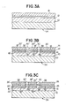
- Figs. 5A to 5F of the drawings show the steps of a modification of the fabrication process hereinbefore described with reference to Figs. 3A to 3E and are also useful for the fabrication of an emitter-coupled logic circuit.
- the process shown in Figs. 5A to 5F starts with preparation of a monocrystalline semi-insulating GaAs substrate 34 having an n-type GaAs epilayer 10, a p-type germanium epilayer 12 and a n-type germanium epilayer 14 as shown in Fig. 5A.
- the semi-insulating GaAs substrate 34, n-type GaAs epilayer 10 and p-type and n-type germanium epilayers 12 and 14 are all similar to those used in the process described with reference to Figs. 3A to 3E with the GaAs epilayer 10 and the germanium epilayers 12 and 14 also formed by molecular beam epitaxy.
- a photoresist is then spun on to the surface of the upper n-type germanium epilayer 14 to form a photoresist coating 46 as shown in Fig. 5B.
- the photoresist coating 46 is patterned and etched to define two collector regions on both sides of a common emitter region of the emitter-coupled logic to be fabricated.
- a p-type dopant such as boron is injected by ion implantation into the unmasked areas of the epilayers 12 and 14 and far into upper surface portions of the area of the GaAs epilayer 10 which underlie the unmasked areas of the germanium epilayers 12 and 14.
- the energy to be used for the ion implantation is selected to assure the p-type dopant to penetrate into the upper surface portion of the area of the GaAs epilayer 10 underlying the p-type germanium epilayer 12.
- the n-type GaAs; epilayer 10 has three doped surface regions 16, 16' and 16", the lower p-type germanium epilayer 12 has three doped regions 18, 18' and 18", and the upper n-type germanium epilayer 14 has three doped regions 20, 20' and 20" in addition to an original unimplanted lower layer region 22 of the GaAs epilayer 10, as shown in Fig. 5B.
- the doped surface regions 16, 16' and 16" of the n-type GaAs epilayer 10 are separated from one another across portions 36 and 36' of the unimplanted lower layer region 22 of the epilayer 10.
- the doped regions 18, 18' and 18" of the lower p-type germanium epilayer 12 overlie the doped surface regions 16, 16' and 16", respectively, of the GaAs epilayer 10 and are separated from one another across unimplanted regions 38 and 38' of the germanium epilayer 12.
- the doped regions 20, 20' and 20" of the upper n-type p-type germanium epilayer 14 overlie the doped regions 18, 18' and 18", respectively, of the lower p-type germanium epilayer 12 and are separated from one another across unimplanted regions 40 and 40' of the germanium epilayer 14.
- the photoresist mask 46 is stripped off upon completion of the ion implantation step.
- ion implantation step is for a second time carried out immediately following the first implantation step.
- a photoresist mask 48 is now used which is patterned to cover not only the collector regions but also the common emitter region of the emitter-coupled logic to be fabricated, as shown in Fig. 5C.
- a p-type dopant of the same type as used in the first implantation step such as boron is implanted into the unmasked areas of the epilayers 12 and 14 and those portions of the GaAs epilayer 10 which underlie the unmasked areas of the epilayers 12 and 14.
- the energy to be used is selected to assure the dopant to reach the interface between the semi-insulating GaAs substrate 34 and the overlying n-type GaAs epilayer 10.
- the initial n-type GaAs epilayer 10 has doped regions 50 and 50' on both sides of a region aligned with the photoresist mask 48.
- the photoresist mask 48 is removed when the ion implantation is complete.
- the resultant semiconductor structure is annealed at a temperature within the range of from 400°C to 600°C to activate the atoms of boron injected into the regions 18 and 18' of the p-type germanium epilayer 12 and the regions 20 and 20' of the n-type germanium epilayer 14 by the first and second ion implantation steps and the atoms of boron injected into the regions 18" and 20" of the p-type and n-type germanium epilayers 12 and 14 by the first ion implantation step.
- the doped regions 20, 20' and 20" of the initial n-type germanium epilayer 14 are thus converted into p-type germanium regions 24, 24' and 24", respectively, and the doped regions 18, 18' and 18" of the initial p-type germanium epilayer 14 become heavily doped p-type germanium regions 26, 26' and 26', respectively, as shown in Fig. 5D.
- the aligned p-type regions 24 and 26 form a base contact or connecting region 42 and, likewise, the aligned: p-type regions 24' and 26' form a base contact or connecting region 42'.
- the regions 50, 50' and 16" doped with boron of the n-type GaAs epilayer 10 are rendered semi-insulating by the implantation step or steps and remain as such after the annealing process, for the reasons explained previously.
- the semi-insulating regions 50 and 50' of the n-type GaAs epilayer 10 have defined therebetween an unimplanted n-type GaAs region 52 which underlies the collector and common emitter forming regions of the initial germanium epilayers 12 and 14.
- a photoresist is then spun on to the surface of the resultant structure to form a photoresist coating 54 on the surface of the toplevel layer forming the regions 24, 24' and 24" and regions 42 and 42'.
- the photoresist coating 54 is patterned and etched to define a desired emitter electrode region through the region 24" between the collector-forming regions 40 and 40' of the toplevel layer as shown in Fig. 5D.
- the remaining photoresist coating 54 is used as a mask to etch the toplevel layer for forming a trench 44 extending through the aligned p-type germanium regions 24" and 26" and the semi-insulating GaAs region 16" to reach the surface of the unimplanted emitter-forming region 52 of the initial n-type .
- GaAs epilayer 10 as shown in Fig. 5E.
- the trench 44 thus formed has its bottom surrounded by a remaining filament of the semi-insulating GaAs -region 16" so that the width of the emitter region to be formed below the trench 44 might not be reduced as a result of the formation of the trench 44.
- a metalization process with, for example, a gold-germanium alloy is then performed to have collector electrode regions 28 and 28' formed on the unimplented regions 40 and 40' of the initial n-type germanium layer 14 and base electrode regions 30 and 30' formed on the p-type germanium regions 24 and 24' forming part of the base contact or connecting portions of the device.
- an emitter electrode layer 32 is formed on the exposed surface of the unimplanted region 52 of the initial n-type GaAs epilayer 10 below the trench 44.
- a pair of n-p-n heterojunction bipolar transistors are thus completed as shown in Fig. 3E and form an emitter-coupled logic circuit as shown in Fig. 4.
- Each of the two bipolar transistors forming each of the emitter-coupled logic circuits fabricated by the process described with reference to Figs. 3A to 3E and the process described with reference to Figs. 5A to 5F has a heterogeneous emitter-base junction between the emitter region 22 ot 52 of n-type GaAs and each of the base regions 38 and 38' of p-type germanium.
- the bandgap of the GaAs forming the emitter region 22 or 52 is approximately 1.42 eV and is thus wider than the bandgap of 0.74 of the germanium forming the active base regions 38 and 38'.
- the edges of the conduction and valence bands of the layers of GaAs and germanium have discontinuities at the heterojunction interface between the layers due to the difference in electronegativity between the two substances.
- the discontinuity in the energy level at the band edge of the conduction band results in an initial velocity of movement of the electrons to be transported from the emitter region 22 or 55 into the active base region 38/38' of each of the transistors. This initial velocity reduces the period of time for which the electrons travel through the overall base region 38-24-26/38'-24'-26' and thus contributes to improvement of the cutoff frequency and accordingly the high-frequency performance of each transistor device.
- the discontinuity in the energy level at the band edge of the valence band results in creation of a barrier to the movement of holes which attempt to enter the emitter region 22 or 52 from the active base region 38/38' and contributes to reduction in the recombination of holes and electrons within the emitter region 22 or 52 and accordingly in the current to result from the recombined carriers, thereby providing an increased electron pumping efficiency across the heterojunction and accordingly the current amplification factor of each device.
- Each of the transistors fabricated in accordance with the present invention thus provides a higher cutoff frequency and a larger load driving capability than homogeneous p-n junction bipolar transistors.
- a heterojunction bipolar transistor fabricated in accordance with the present invention is further characterized for its contact or connecting base regions 42 and 42' in part resulting from the initial p-type germanium epilayer 12 which is doped with a p-type dopant to add to the carrier concentration in the layer.
- the transistor device has a graft base configuration contributing to reduction in the parasitic resistance through the base region.
- a graft base configuration invites an increase in the parasitic capacitance of the base-emitter junction interface and thus impairs the performance quality of the device per se.
- Such a problem is eliminated in a heterojunction bipolar transistor fabricated in accordance with the present invention since the contact or connecting base regions 42 and 42' are isolated from the emitter region 22 or 52 by means of the initial n-type GaAs epilayer 10 which intervenes between the emitter region and the contact or connection base regions and which is rendered semi-insulating by the implant of a p-type dopant such as boron.
- the overall configuration of the transistor device fabricated by the process described with reference to Figs. 3A to 3E or Figs. 5A to 5F is particularly useful for the construction of an emitter-coupled logic circuit having no interconnection between separate emitter regions. If desired, however, the transistor device which has been described as being to be used as an emitter-coupled logic as shown in Fig. 4 may be used as a single transistor having both of its bases interconnected and both of its collectors interconnected. Such a single transistor device will prove useful for high-frequency applications using 1 giga hertz or more.
- the heterojunction in a transistor device proposed by the present invention is to be formed by the combination of GaAs and germanium
- an essentially similar effect will be achieved by the use of the combination of gallium phosphide (GaP) in substitution for GaAs and silicon in lieu of germanium.
- GaP gallium phosphide
- Using the combination of galium phosphide and silicon will particularly advantageous in an emitter-coupled logic circuit fabricated as by the process described with reference to Figs. 5A to 5F.
- the emitter-coupled logic circuit fabricated by the fabrication process therein shown is surrounded by the boron-implanted semi-insulating regions 50 and 50' and is thereby isolated from another device or another device combination which may be fabricated on the same substrate.
- FIG. 6 of the drawings shows forward voltage-current density characteristic curves "A" and "B” for a heterojunction formed by p-type silicon and n-type gallium phosphide without implantation of boron and a heterojunction formed by p-type silicon and n-type gallium phosphide which is rendered semi-insulating with the implantation of boron.
- Fig. 7 shows similar curves "C” and "D” for a heterojunction formed by p-type germanium and n-type GaAs without implantation of boron and a heterojunction formed by p-type germanium and n-type GaAs rendered semi-insulating with the implantation of boron. From comparison between Figs.
- Fig. 8 of the drawings shows the relationship between the forward voltage and the ratio of the current density achieved without implantation of boron versus the current density achieved with implantation of boron for the combination of p-type silicon and n-type gallium phosphide as indicated by curve "E" and the combination of p-type germanium and n-type GaAs as indicated by curve "F".
Abstract
Description
- The present invention relates to semiconductor devices and, more particularly, to a heterojunction bipolar transistor device. The present invention further relates to a process of fabricating a semiconductor device, particularly, a heterojunction bipolar transistor device or a unit circuit such as an emitter-coupled logic composed of heterojunction bipolar transistors.
- Semiconductor devices presently known and in use are broken down to three major categories of homogeneous pn junction devices, Schottky barrier devices and metal-oxide-semiconductor (MOS) devices. Typical of homogeneous pn junction devices are bipolar transistors. Bipolar transistors are contrasted by unipolar or field-effect transistors which may be of any of the homogeneous pn junction, Schottky barrier and metal-oxide-semiconductor configurations. The high-frequency performance of a unipolar transistors can be improved by microminiaturization of the' gate of the device while that of a bipolar transistor improved by reducing the thickness of the base region of the device. In whichsoever case, it is important that the devices be designed and fabricated with a view to reducing the parasitic resistances and capacitances to be involved in the devices. For this purpose, it is of particular significance to reduce the source/gate and drain/gate resistances for transistors of the unipolar type and the base resistances and the emitter/base capacitances for bipolar transistors.
- In a semiconductor integrated circuit composed of a number of transistors provided as component devices, unipolar transistors excel bipolar transistors for their smaller power dissipation rates but are inferior to the latter for their capabilities to drive loads. Where load driving capabilities are among preferential requirements of component devices forming a semiconductor integrated circuit, bipolar transistors are used almost exclusively over unipolar devices. Bipolar transistors are generally fabricated of silicon and provide high-frequency performances having limitations represented by cutoff frequencies of from It giga hertz to 20 giga hertz as well known in the art.
- Vigorous research and development efforts are being thus made for integrated circuits composed of field-effect transistors using gallium-arsenide providing an electron mobility which is three to five times higher than that achievable by silicon. As well known in the art, field-effect transistors of gallium-arsenide provide higher cutoff frequencies as they are scaled down. The increased cutoff frequency will do justice to a semiconductor integrated circuit with a relatively small load requirement and a relatively low integration density. It is, however, presumed by those skilled in the art that increasing the density of the integrated circuit as achieved by the miniaturization of the component devices might be detrimental to achievement of faster operation because of the low load driving capabilities of the field-effect transistors. There is, for this reason, a . demand for transistors providing increased load driving capabilities or, more specifically, for bipolar transistors having improved cutoff frequency characteristics. A prime object of the present invention is to provide a bipolar transistor with an increased cutoff frequency and more adaptability to integration and a process of fabricating such a transistor.
- In accordance with the present invention, there is provided a bipolar transistor comprising a) a first layer of a first semiconductor material having a first conductivity type, b) a second layer on the first layer,'the second layer being of a second semiconductor material having a second conductivity type opposite to the first conductivity type, the second semiconductor material having an energy bandgap less than that of the first semiconductor material, c) a third layer on the second layer, the third layer being of the second semiconductor material and having the first conductivity type, d) a first doped region in the first layer, the first doped region being of the first semiconductor material and being doped to be semi-insulating regions, and e) a second doped region in the third layer, the second doped region being of the second semiconductor material and being doped to the second conductivity type, f) the second layer having a portion forming an active base region, the third layer having a portion forming a collector region in contact with the active base region, the first doped region defining in the first layer an active emitter region in contact with the active base region, the second doped region forming a connecting base region electrically coupled with the active base region.
- In accordance with another outstanding aspect of the present invention, there is provided a process of fabricating a bipolar transistor, comprising the steps of a) epitaxially forming a first layer of a first semiconductor material having a first conductivity type, b) epitaxially forming on the first layer a second layer of a second semiconductor material having a second conductivity type opposite to the first conductivity type, the second layer having a portion for forming an active base region, the second semiconductor material having an energy bandgap less than that of the first semiconductor material, c) epitaxially forming on the second layer a third layer of the second semiconductor material and having the first conductivity type, the third layer having a portion for forming a collector region in contact with the active base region, and d) introducing a dopant of the second conductivity type into a portion of the third layer and through the second layer into a portion of the first layer, e) heating the resultant structure for converting the doped portion of the first layer into a semi-insulating region and converting the doped portion of the third layer into a doped region having the second conductivity type, the semi-insulating region defining in the first layer an active emitter region in contact with the active base region, the doped region of the third layer forming a connecting base region electrically coupled with the active base region.
- The features and advantages of a transistor device according to the present invention will be more clearly appreciated from the following description taken in conjunction with the accompanying drawings in which like reference numerals designate similar or corresponding elements, portions and regions and in which:
- Figs. 1A to lE are fragmentary cross sectional views showing major process steps of a process of fabricating a preferred embodiment of a transistor device according to the present invention;
- Figs. 2A and 2B are fragmentary cross sectional views showing major process steps of a process of fabricating a modification of the transistor device fabricated by the process shown in Figs. 1A to lE;
- Figs. 3A to 3F are fragmentary cross sectional views showing major process steps of a process of fabricating another preferred embodiment of a semiconductor device according to the present invention;
- Fig. 4 is a schematic view showing the equivalent circuit representative of the emitter-coupled logic provided by the semiconductor device fabricated by the process shown in Figs. 3A to 3F;
- Figs. 5A to 5E are fragmentary cross sectional views showing major process steps of a process of fabricating a modification of the semiconductor device fabricated by the process shown in Figs. 3A to 3F; and
- Fig. 6 is a graph showing forward voltage-current density characteristic curves for a heterojunction formed by p-type silicon and n-type gallium phosphide without implantation of boron (curve "A") and a heterojunction formed by p-type silicon and n-type gallium phosphide which is rendered semi-insulating with the implantation of boron (curve "B");
- Fig. 7 is a graph showing curves similar to those of Fig. 6 but for a heterojunction formed by p-type germanium and n-type gallium-arsenide without implantation of boron (curve "C") and a heterojunction formed by p-type germanium and n-type gallium-arsenide rendered semi-insulating with the implantation of boron (curve "D");
- Fig. 8 is a graph showing the relationship between the forward voltage and the ratio of the current density achieved' without implantation of a p-type dopant versus the current density achieved with implanmtation of a p-type dopant for the combination of p-type silicon and n-type gallium phosphide (curve "E") and the combination of p-type germanium and n-type gallium-arsenide (curve "F").
- A preferred example of a process of fabricating a transistor device in accordance with the present invention will be hereinafter described with reference to Figs. lA to lE of the drawing.
- The shown example of a process according to the present invention starts with preparation of an n-
type epilayer 10 of GaAs (hereinafter referred to as GaAs). On this n-type GaAs epilayer 10 is grown a p-typemonocrystalline germanium epilayer 12 by, for example, molecular beam epitaxy (MBE), whereupon an n-typemonocrystalline germanium epilayer 14 is grown on the p-type germanium epilayer 12 also by molecular beam epitaxy. Fig. 1A shows the semiconductor structure thus obtained, wherein a heterojunction is formed between the n-type GaAs epilayer 10 which is to result, in part, in an emitter region and the p-type germanium epilayer 12 which is to result, in part, in an active base region as the process advances. - Though not shown in the drawings, a photoresist is spun on to the surface of the upper n-
type germanium epilayer 14 and the resultant photoresist coating is patterned and etched to define a desired device region of the transistor device to be fabricated. The upper twogermanium epilayers epilayers type germanium epilayer 14 of the land thus formed on the n-type GaAs epilayer 10 is covered with a mask (not shown) defining a collector region of the transistor device to be fabricated. A p-type dopant such as boron is injected by ion implantation into the unmasked areas of theepilayers type GaAs epilayer 10 surrounding the land of thegermanium epilayers GaAs epilayer 10 which underlies the p-type germanium epilayer 12. In this instance, the energy to be used for the ion implantation is selected to assure the p-type dopant to reach into the upper surface portion of the area of theGaAs epilayer 10 underlying the p-type germanium epilayer 12. Thus, the n-type GaAs epilayer 10 has adoped surface region 16, the lower p-type germanium epilayer 12 has adoped region 18, and the upper n-type germanium epilayer 14 has adoped region 20, in addition to an original unimplantedlower layer region 22 underlying thedoped surface region 16 of theGaAs epilayer 10, as shown in Fig. 1C. - The resultant semiconductor structure is annealed at a temperature within the range of from 400°C to 600°C so that the atoms of boron injected into each of the
regions doped region 20 of the upper n-type germanium epilayer 14 is thus converted into a p-type germanium region 24, and thedoped region 18 of the lower p-type-germanium epilayer 14 becomes a heavily doped p-type germanium region 26, as shown in Fig. 1D. These coextensive or aligned p-type germanium regions surface region 16 doped with boron of the n-type GaAs epilayer 10 becomes semi-insulating as a result of the injection of the dopant due to the implant damage caused therein. The semi-insulating GaAsregion 16 remain as such after the annealing process because the annealing temperature lower than 600°C is short of activating the atoms of boron injected into theregion 16 of the n-type GaAs epilayer 10 and because the implant damage as caused by the implantation of boron into theGaAs epilayer 10 remains unrelieved by the annealing process. A collector region is defined by the region surrounded by the doped p-type germanium region 24 of the initial n-type germanium epilayer 14, and an active base region is defined by the region surrounded by the heavily doped p-type germanium region 26 of the initial p-type germanium epilayer 12 which is. That portion of theregion 22 of the initial n-type GaAs epilayer 10 which directly underlies this active base region and which is surrounded by thesemi-insulating surface region 16 of theGaAs epilayer 10 defines the effective width of the emitter region, as will be seen from Fig. 1D. The effective width of the emitter region is thus dictated by the boundary of thesemi-insulating surface region 16 of GaAs contiguous with the emitter region directly underlying theactive base region 12 of p-type germanium. An n-p-n heterojunction bipolar transistor (HBT) is completed with acollector electrode layer 28 formed on thecollector region 14, abase electrode layer 30 formed on the base contact or connecting portion provided by the aligned p-type germanium regions emitter electrode layer 32 formed on the reverse surface of the n-type GaAs epilayer 10 as shown in Fig. lE. These electrode layers may be formed by a metalization process with, for example, a gold-germanium alloy. The bipolar transistor has a heterogeneous emitter-base junction interface between the n-type GaAs epilayer 10 and the p-type germanium region 12. - In the heterojunction bipolar transistor thus fabricated, the" bandgap of the emitter,
region 22 of the n-type GaAs epilayer 10 is wider than that of the p-type germanium epilayer 12 forming the active base region so that the edges of the conduction and valence bands of the two layers have discontinuities at the heterojunction interface between the layers. The discontinuity in the energy level at the band edge of the conduction band results in an initial velocity of movement of the electrons to be transported from theemitter region 14 into the active base region -12 of the transistor. This initial velocity reduces the period of time for which the electrons travel through the overall base region and thus contributes to improvement of the high-frequency performance of the device. On the other hand, the discontinuity in the energy level at the band edge of the valence band results in creation of a barrier to the movement of holes which attempt to enter theemitter region 14 from theactive base region 12 and contributes to reduction in the recombination of holes and electrons within theemitter region 14, thereby providing an increased electron pumping efficiency across the heterojunction interface between thelayers - As a result of the annealing process which is carried out subsequently to the ion implantation with boron, the atoms of boron injected into the defined region of the initial n-
type germanium epilayer 14 convert the dopedregion 20 of theepilayer 14 into the p-type germanium region 24 and the atoms of boron injected into the defined region the initial p-type germanium epilayer 12 convert the dopedregion 18 of theepilayer 12 into the p +-type germanium region 26. On the other hand, the atoms of boron injected into the initial n-type GaAs epilayer 10 render the dopedsurface region 16 semi-insulating and are thus conducive to reducing the effective area of the base-emitter junction and the base spreading resistance of the device, viz., the resistance through the extrinsic, viz., contact or connecting base portion formed by the aligned p-type germanium regions - The bipolar transistor device fabricated as hereinbefore described is further advantageous in that the active emitter region is aligned with the collector region across the active base region and is thus substantially coextensive with the collector region due to the formation of the boron-implanted semi-insulating region around the active emitter region.
- Because, furthermore, of the fact that the
emitter electrode layer 32 is attached to the reverse surface of the n-type GaAs epilayer 10, the bipolar transistor, when used in the form of grounded-emitter connection, produces a limited emitter inductance which would otherwise impair the high-frequency performance characteristics of the device. If desired, however, a bipolar transistor according to the present invention may have an emitter electrode layer or two or more emitter electrode regions provided on the upper surface of the device structure. For this purpose, the fabrication process step resulting in the structure shown in Fig. 1B may be followed by formation of a mask patterned to cover not only the central portion of the upper n-type germanium epilayer 14 as described but also at least one portion of the n-type GaAs epilayer 10 within the area in which the transistor device is to be fabricated. A p-type dopant such as boron is then injected by ion implantation into the unmasked areas of the p-type and n-type germanium epilayers type germanium epilayer 12, and the exposed area of the GaAs epilayer 10 as shown in Fig. 2A. Thus, the n-type GaAs epilayer 10 has an undoped region 22' partly exposed at the upper surface of theepilayer 10 as well as the dopedsurface region 16 of GaAs in part underlying the dopedgermanium regions epilayer 10. The resultant structure is annealed as discussed previously so that the atoms of the p-type dopant injected into each of theregions type germanium region 24 and the heavily doped p-type germanium region 26, respectively, as shown in Fig. 2B. An n-p-n bipolar transistor is thus obtained with acollector electrode layer 28 formed on thecollector region 14, a baseelectrode layer region 30 formed on theactive base region 12 and an emitter electrode layer region 32' formed on the upper surface of the n-type GaAs epilayer 10. - The process according to the present invention as hereinbefore described can be modified for the fabrication of an emitter-coupled logic (ECL) circuit. Some of the steps required to carry out in such a process are shown in Figs. 3A to 3E of the drawings.
- The process shown in Figs. 3A to 3E starts with preparation of a
monocrystalline GaAs substrate 34 doped with, for example, chromium to be semi-insulating. An epilayer is grown on thissemi-insulating GaAs substrate 34 and doped with, for example, silicon to a carrier concentration of 1x10¹⁸ atoms/cm-3 to form an n-type GaAs epilayer 10. On this n-type GaAs epilayer 10 is grown amonocrystalline germanium epilayer 12 to a thickness of 0.1 micron by molecular beam epitaxy and is doped with, for example, boron to a carrier concentration of 1x10¹⁷ atoms/cm-3. Thereupon, amonocrystalline germanium epilayer 14 is grown on the p-type germanium epilayer 12 to a thickness of 0.6 micron also by molecular beam epitaxy and is doped with, for example, phosphorus to a carrier concentration of 1x10¹⁶ atoms/cm-3. Fig. 3A shows the semiconductor structure thus obtained. In the structure shown in Fig. 3A, a heterojunction is formed between the n-type GaAs epilayer 10 which is to result, in part, in two collector regions and the p-type germanium epilayer 12 which is to result, in part, in two active base regions as the process advances. - A photoresist is then spun on to the surface of the upper n-
type germanium epilayer 14 to form a photoresist coating (not shown). The photoresist coating is patterned and etched to define two collector regions on both sides of a common emitter region of the emitter-coupled logic to be fabricated. A p-type dopant such as boron is injected by ion implantation into the unmasked areas of theepilayers type GaAs epilayer 10 underlying the unmasked areas of the germanium epilayers 12 and 14. In this instance, the energy to be used for the ion implantation is selected to assure the p-type dopant to penetrate into the upper surface portions of theGaAs epilayer 10 underlying the germanium epilayers 12 and 14. As a consequence of this ion implantation step, the n-type GaAs epilayer 10 has three dopedsurface regions type germanium epilayer 12 has three dopedregions type germanium epilayer 14 has three dopedregions lower layer region 22 of theGaAs epilayer 10, as shown in Fig. 3B. The dopedsurface regions type GaAs epilayer 10 are separated from one another acrossportions 36 and 36' of the unimplantedlower layer region 22 of theepilayer 10. The dopedregions type germanium epilayer 12 overlie the dopedsurface regions unimplanted regions 38 and 38' of thegermanium epilayer 12. The dopedregions type germanium epilayer 14 overlie the dopedregions type germanium epilayer 12 and are separated from one another acrossunimplanted regions 40 and 40' of thegermanium epilayer 14. Theunimplanted region 22 of the n-type GaAs epilayer 10 is to result in the common emitter region, and theunimplanted regions 38 and 38' of the p-type germanium epilayer 12 are to result in the active base regions, respectively, of the emitter-coupled logic circuit. Theunimplanted regions 40 and 40' of the n-type germanium epilayer 14 are to result in the collector regions, respectively, of the emitter-coupled logic circuit. Implantation-of boron far into the n-type GaAs epilayer 10 to form the dopedsurface regions epilayer 10 as discussed above is of particular importance since the geometries, viz., the width and length of the common emitter region to be formed are dictated by the geometries, viz., the width and length of the two collector regions to result from theunimplanted regions 40 and 40', respectively, of the n-type germanium epilayer 14. - The resultant semiconductor structure is annealed at a temperature within the range of from 400°C to 600°C so that the atoms of boron injected into the
regions type germanium epilayer 12 and theregions type germanium epilayer 14 are thermally activated. The dopedregions type germanium epilayer 14 are thus converted into p-type germanium regions regions type germanium epilayer 14 become heavily doped p-type germanium regions type regions region 42 of one of the transistors to form the emitter-coupled logic and, likewise, the aligned p-type regions 24' and 26' form in combination a base contact or connecting region 42' 'of the other transistor of the emitter-coupled logic. On the other hand, theregions type GaAs epilayer 10 are rendered semi-insulating by the injection of the dopant due to the implant damage caused therein. As noted previously, these semi-insulating GaAs regions remain as such after the annealing process because the atoms of boron injected into these regions can not be activated by the annealing at a temperature lower than 600°C and because the implant damage as caused by the implantation of boron into the GaAs epilayer 10 remains unrelieved by the annealing process, as previously noted. Thesesemi-insulating GaAs regions regions 42 and 42' from the unimplanted emitter-formingregion 22 of the n-type GaAs epilayer 10. - A photoresist is then spun on to the surface of the resultant structure to form a photoresist coating (not shown) on the surface of the toplevel layer forming the
regions regions 42 and 42'. The photoresist coating is patterned and etched to define a desired emitter electrode region through theregion 24" between the collector-formingregions 40 and 40' of the toplevel layer. The remaining photoresist coating is used as a mask to etch the toplevel layer for forming atrench 44 extending through the aligned p-type germanium regions 24" and 26" and thesemi-insulating GaAs region 16" to reach the surface of the unimplanted emitter-formingregion 22 of the initial n-type GaAs epilayer 10 as shown in Fig. 3D. Thetrench 44 thus formed has its bottom surrounded by a remaining filament of the semi-insulating GaAs region' 16" so that the width of the emitter region to be formed below thetrench 44 might not be reduced as a result of the formation of thetrench 44. A pair of n-p-n heterojunction bipolar transistors are thus completed by a metalization process with, for example, a gold-germanium alloy. Thus,collector electrode regions 28 and 28' are formed on theunimplanted regions 40 and 40' of the initial n-type germanium layer 14 andbase electrode regions 30 and 30' are formed on the p-type germanium regions emitter electrode layer 32 is formed on the exposed surface of theunimplanted region 22 of the initial n-type GaAs epilayer 10 below the trench as shown in Fig. 3E. These two bipolar transistors form an emitter-coupled logic circuit having thecollector regions 40 and 40' separate from each other across thetrench 44, theactive base regions 38 and 38' also separate from each other across thetrench 44, andcommon emitter region 22 below thetrench 44, as shown in Fig. 4. Each of these two bipolar transistors has a heterogeneous emitter-base junction between theemitter region 22 of n-type GaAs and each of thebase regions 38 and 38' of p-type germanium. - Figs. 5A to 5F of the drawings show the steps of a modification of the fabrication process hereinbefore described with reference to Figs. 3A to 3E and are also useful for the fabrication of an emitter-coupled logic circuit.
- The process shown in Figs. 5A to 5F starts with preparation of a monocrystalline
semi-insulating GaAs substrate 34 having an n-type GaAs epilayer 10, a p-type germanium epilayer 12 and a n-type germanium epilayer 14 as shown in Fig. 5A. Thesemi-insulating GaAs substrate 34, n-type GaAs epilayer 10 and p-type and n-type germanium epilayers - A photoresist is then spun on to the surface of the upper n-
type germanium epilayer 14 to form aphotoresist coating 46 as shown in Fig. 5B. Thephotoresist coating 46 is patterned and etched to define two collector regions on both sides of a common emitter region of the emitter-coupled logic to be fabricated. With the patterned photoresist coating 46 -used as a mask, a p-type dopant such as boron is injected by ion implantation into the unmasked areas of theepilayers GaAs epilayer 10 underlying the p-type germanium epilayer 12. In the process herein shown, it is further important that the penetration depth of the ions injected into the semiconductor structure be controlled so that the ions will not penetrate throughout the thickness of the n-type GaAs epilayer 10 and reach thesemi-insulating GaAs substrate 34. As a result of this ion implantation step, the n-type GaAs;epilayer 10 has three dopedsurface regions type germanium epilayer 12 has three dopedregions type germanium epilayer 14 has three dopedregions lower layer region 22 of theGaAs epilayer 10, as shown in Fig. 5B. The dopedsurface regions type GaAs epilayer 10 are separated from one another acrossportions 36 and 36' of the unimplantedlower layer region 22 of theepilayer 10. The dopedregions type germanium epilayer 12 overlie the dopedsurface regions unimplanted regions 38 and 38' of thegermanium epilayer 12. The dopedregions type germanium epilayer 14 overlie the dopedregions type germanium epilayer 12 and are separated from one another acrossunimplanted regions 40 and 40' of thegermanium epilayer 14. Thephotoresist mask 46 is stripped off upon completion of the ion implantation step. - In the modified process according to the present invention, ion implantation step is for a second time carried out immediately following the first implantation step. A
photoresist mask 48 is now used which is patterned to cover not only the collector regions but also the common emitter region of the emitter-coupled logic to be fabricated, as shown in Fig. 5C. Using this patternedphotoresist mask 48, a p-type dopant of the same type as used in the first implantation step such as boron is implanted into the unmasked areas of theepilayers epilayers semi-insulating GaAs substrate 34 and the overlying n-type GaAs epilayer 10. Thus, the initial n-type GaAs epilayer 10 has dopedregions 50 and 50' on both sides of a region aligned with thephotoresist mask 48. Thephotoresist mask 48 is removed when the ion implantation is complete. - The resultant semiconductor structure is annealed at a temperature within the range of from 400°C to 600°C to activate the atoms of boron injected into the
regions 18 and 18' of the p-type germanium epilayer 12 and theregions 20 and 20' of the n-type germanium epilayer 14 by the first and second ion implantation steps and the atoms of boron injected into theregions 18" and 20" of the p-type and n-type germanium epilayers regions type germanium epilayer 14 are thus converted into p-type germanium regions regions type germanium epilayer 14 become heavily doped p-type germanium regions 26, 26' and 26', respectively, as shown in Fig. 5D. The aligned p-type regions region 42 and, likewise, the aligned: p-type regions 24' and 26' form a base contact or connecting region 42'. On the other hand, theregions type GaAs epilayer 10 are rendered semi-insulating by the implantation step or steps and remain as such after the annealing process, for the reasons explained previously. Thesemi-insulating regions 50 and 50' of the n-type GaAs epilayer 10 have defined therebetween an unimplanted n-type GaAs region 52 which underlies the collector and common emitter forming regions of theinitial germanium epilayers - A photoresist is then spun on to the surface of the resultant structure to form a
photoresist coating 54 on the surface of the toplevel layer forming theregions regions 42 and 42'. Thephotoresist coating 54 is patterned and etched to define a desired emitter electrode region through theregion 24" between the collector-formingregions 40 and 40' of the toplevel layer as shown in Fig. 5D. The remainingphotoresist coating 54 is used as a mask to etch the toplevel layer for forming atrench 44 extending through the aligned p-type germanium regions 24" and 26" and thesemi-insulating GaAs region 16" to reach the surface of the unimplanted emitter-formingregion 52 of the initial n-type .GaAs epilayer 10 as shown in Fig. 5E. Thetrench 44 thus formed has its bottom surrounded by a remaining filament of the semi-insulating GaAs -region 16" so that the width of the emitter region to be formed below thetrench 44 might not be reduced as a result of the formation of thetrench 44. A metalization process with, for example, a gold-germanium alloy is then performed to havecollector electrode regions 28 and 28' formed on theunimplented regions 40 and 40' of the initial n-type germanium layer 14 andbase electrode regions 30 and 30' formed on the p-type germanium regions emitter electrode layer 32 is formed on the exposed surface of theunimplanted region 52 of the initial n-type GaAs epilayer 10 below thetrench 44. A pair of n-p-n heterojunction bipolar transistors are thus completed as shown in Fig. 3E and form an emitter-coupled logic circuit as shown in Fig. 4. - Each of the two bipolar transistors forming each of the emitter-coupled logic circuits fabricated by the process described with reference to Figs. 3A to 3E and the process described with reference to Figs. 5A to 5F has a heterogeneous emitter-base junction between the
emitter region 22ot 52 of n-type GaAs and each of thebase regions 38 and 38' of p-type germanium. The bandgap of the GaAs forming theemitter region active base regions 38 and 38'. The edges of the conduction and valence bands of the layers of GaAs and germanium have discontinuities at the heterojunction interface between the layers due to the difference in electronegativity between the two substances. The discontinuity in the energy level at the band edge of the conduction band results in an initial velocity of movement of the electrons to be transported from theemitter region 22 or 55 into theactive base region 38/38' of each of the transistors. This initial velocity reduces the period of time for which the electrons travel through the overall base region 38-24-26/38'-24'-26' and thus contributes to improvement of the cutoff frequency and accordingly the high-frequency performance of each transistor device. On the other hand, the discontinuity in the energy level at the band edge of the valence band results in creation of a barrier to the movement of holes which attempt to enter theemitter region active base region 38/38' and contributes to reduction in the recombination of holes and electrons within theemitter region - A heterojunction bipolar transistor fabricated in accordance with the present invention is further characterized for its contact or connecting
base regions 42 and 42' in part resulting from the initial p-type germanium epilayer 12 which is doped with a p-type dopant to add to the carrier concentration in the layer. Thus, the transistor device has a graft base configuration contributing to reduction in the parasitic resistance through the base region. As well known in the art, it is inevitable in a silicon bipolar transistor device that a graft base configuration invites an increase in the parasitic capacitance of the base-emitter junction interface and thus impairs the performance quality of the device per se. Such a problem is eliminated in a heterojunction bipolar transistor fabricated in accordance with the present invention since the contact or connectingbase regions 42 and 42' are isolated from theemitter region type GaAs epilayer 10 which intervenes between the emitter region and the contact or connection base regions and which is rendered semi-insulating by the implant of a p-type dopant such as boron. - The overall configuration of the transistor device fabricated by the process described with reference to Figs. 3A to 3E or Figs. 5A to 5F is particularly useful for the construction of an emitter-coupled logic circuit having no interconnection between separate emitter regions. If desired, however, the transistor device which has been described as being to be used as an emitter-coupled logic as shown in Fig. 4 may be used as a single transistor having both of its bases interconnected and both of its collectors interconnected. Such a single transistor device will prove useful for high-frequency applications using 1 giga hertz or more.
- While it has been assumed that the heterojunction in a transistor device proposed by the present invention is to be formed by the combination of GaAs and germanium, an essentially similar effect will be achieved by the use of the combination of gallium phosphide (GaP) in substitution for GaAs and silicon in lieu of germanium. Using the combination of galium phosphide and silicon will particularly advantageous in an emitter-coupled logic circuit fabricated as by the process described with reference to Figs. 5A to 5F. The emitter-coupled logic circuit fabricated by the fabrication process therein shown is surrounded by the boron-implanted
semi-insulating regions 50 and 50' and is thereby isolated from another device or another device combination which may be fabricated on the same substrate. Fig. 6 of the drawings shows forward voltage-current density characteristic curves "A" and "B" for a heterojunction formed by p-type silicon and n-type gallium phosphide without implantation of boron and a heterojunction formed by p-type silicon and n-type gallium phosphide which is rendered semi-insulating with the implantation of boron. Fig. 7 shows similar curves "C" and "D" for a heterojunction formed by p-type germanium and n-type GaAs without implantation of boron and a heterojunction formed by p-type germanium and n-type GaAs rendered semi-insulating with the implantation of boron. From comparison between Figs. 6 and 7 it will be seen that the combination of p-type silicon and n-type gallium phosphide is capable of achieving reduction of the order of four digits in the current density by the implantation of boron and is thus more advantageous for device isolation than the combination of p-type germanium and n-type GaAs. On the other hand, Fig. 8 of the drawings shows the relationship between the forward voltage and the ratio of the current density achieved without implantation of boron versus the current density achieved with implantation of boron for the combination of p-type silicon and n-type gallium phosphide as indicated by curve "E" and the combination of p-type germanium and n-type GaAs as indicated by curve "F". These curves "E" and "F" evidence that the combination of p-type silicon and n-type gallium phosphide for device isolation purposes than the combination of p-type germanium and n-type GaAs where implantation with boron is used.
Claims (13)
Applications Claiming Priority (4)
| Application Number | Priority Date | Filing Date | Title |
|---|---|---|---|
| JP59957/85 | 1985-03-25 | ||
| JP5995785 | 1985-03-25 | ||
| JP59958/85 | 1985-03-25 | ||
| JP5995885 | 1985-03-25 |
Publications (3)
| Publication Number | Publication Date |
|---|---|
| EP0197424A2 true EP0197424A2 (en) | 1986-10-15 |
| EP0197424A3 EP0197424A3 (en) | 1988-05-25 |
| EP0197424B1 EP0197424B1 (en) | 1993-06-02 |
Family
ID=26401021
Family Applications (1)
| Application Number | Title | Priority Date | Filing Date |
|---|---|---|---|
| EP86104067A Expired - Lifetime EP0197424B1 (en) | 1985-03-25 | 1986-03-25 | Process of fabricating a heterojunction bipolar transistor |
Country Status (4)
| Country | Link |
|---|---|
| US (1) | US4823174A (en) |
| EP (1) | EP0197424B1 (en) |
| JP (1) | JP2553510B2 (en) |
| DE (1) | DE3688516T2 (en) |
Cited By (1)
| Publication number | Priority date | Publication date | Assignee | Title |
|---|---|---|---|---|
| EP0288681A1 (en) * | 1987-04-23 | 1988-11-02 | International Business Machines Corporation | Heterojunction bipolar transistor |
Families Citing this family (8)
| Publication number | Priority date | Publication date | Assignee | Title |
|---|---|---|---|---|
| US4970578A (en) * | 1987-05-01 | 1990-11-13 | Raytheon Company | Selective backside plating of GaAs monolithic microwave integrated circuits |
| US5939738A (en) * | 1995-10-25 | 1999-08-17 | Texas Instruments Incorporated | Low base-resistance bipolar transistor |
| JP3086906B1 (en) | 1999-05-28 | 2000-09-11 | 工業技術院長 | Field effect transistor and method of manufacturing the same |
| KR100332106B1 (en) * | 1999-06-29 | 2002-04-10 | 박종섭 | Method of manufacturing a transistor in a semiconductor device |
| JP3425603B2 (en) | 2000-01-28 | 2003-07-14 | 独立行政法人産業技術総合研究所 | Method for manufacturing field effect transistor |
| US7359888B2 (en) * | 2003-01-31 | 2008-04-15 | Hewlett-Packard Development Company, L.P. | Molecular-junction-nanowire-crossbar-based neural network |
| US7705625B2 (en) * | 2005-07-08 | 2010-04-27 | Zmos Technology, Inc. | Source transistor configurations and control methods |
| US8894504B1 (en) * | 2013-01-16 | 2014-11-25 | Stacy Keisler | Golf putting training device |
Citations (3)
| Publication number | Priority date | Publication date | Assignee | Title |
|---|---|---|---|---|
| GB1499561A (en) * | 1974-01-18 | 1978-02-01 | Univ Connecticut | Heterojunction devices |
| US4380774A (en) * | 1980-12-19 | 1983-04-19 | The United States Of America As Represented By The Secretary Of The Navy | High-performance bipolar microwave transistor |
| EP0130774A1 (en) * | 1983-06-30 | 1985-01-09 | Fujitsu Limited | Process for fabricating bipolar transistor |
Family Cites Families (1)
| Publication number | Priority date | Publication date | Assignee | Title |
|---|---|---|---|---|
| US4611388A (en) * | 1983-04-14 | 1986-09-16 | Allied Corporation | Method of forming an indium phosphide-boron phosphide heterojunction bipolar transistor |
-
1986
- 1986-03-25 DE DE86104067T patent/DE3688516T2/en not_active Expired - Lifetime
- 1986-03-25 EP EP86104067A patent/EP0197424B1/en not_active Expired - Lifetime
- 1986-03-25 JP JP61067834A patent/JP2553510B2/en not_active Expired - Fee Related
-
1988
- 1988-06-08 US US07/205,573 patent/US4823174A/en not_active Expired - Lifetime
Patent Citations (3)
| Publication number | Priority date | Publication date | Assignee | Title |
|---|---|---|---|---|
| GB1499561A (en) * | 1974-01-18 | 1978-02-01 | Univ Connecticut | Heterojunction devices |
| US4380774A (en) * | 1980-12-19 | 1983-04-19 | The United States Of America As Represented By The Secretary Of The Navy | High-performance bipolar microwave transistor |
| EP0130774A1 (en) * | 1983-06-30 | 1985-01-09 | Fujitsu Limited | Process for fabricating bipolar transistor |
Non-Patent Citations (3)
| Title |
|---|
| IEEE ELECTRON DEVICE LETTERS, vol. EDL-3, no. 2, February 1982, pages 43-45, New York, US; W. McLEVIGE et al.: "GaAs/AlGaAs heterojunction bipolar transistors for integrated circuit applications" * |
| IEEE ELECTRON DEVICE LETTERS, vol. EDL-5, no. 3, March 1984, pages 99-100, New York, US; C. FONSTAD "Consideration of the relative frequency performance potential of inverted heterojunction n-p-n transistors" * |
| JOURNAL OF THE ELECTROCHEMICAL SOCIETY, vol. 132, no. 6, June 1985, abstract no. 728 S0A, page 220C, Manchester, US; T. ITOH et al.: "Ge/GaAs Heterojunction for bipolar transistors" * |
Cited By (1)
| Publication number | Priority date | Publication date | Assignee | Title |
|---|---|---|---|---|
| EP0288681A1 (en) * | 1987-04-23 | 1988-11-02 | International Business Machines Corporation | Heterojunction bipolar transistor |
Also Published As
| Publication number | Publication date |
|---|---|
| US4823174A (en) | 1989-04-18 |
| DE3688516T2 (en) | 1993-10-07 |
| EP0197424A3 (en) | 1988-05-25 |
| JPS621270A (en) | 1987-01-07 |
| JP2553510B2 (en) | 1996-11-13 |
| DE3688516D1 (en) | 1993-07-08 |
| EP0197424B1 (en) | 1993-06-02 |
Similar Documents
| Publication | Publication Date | Title |
|---|---|---|
| US5656514A (en) | Method for making heterojunction bipolar transistor with self-aligned retrograde emitter profile | |
| US4683487A (en) | Heterojunction bipolar transistor | |
| US5422502A (en) | Lateral bipolar transistor | |
| US5324671A (en) | Method of fabrication an integrated circuit including bipolar and field effect devices | |
| US4924283A (en) | Heterojunction bipolar transistor and process for fabricating same | |
| US5147775A (en) | Method of fabricating a high-frequency bipolar transistor | |
| JPH06163567A (en) | P-n junction diffusion barrier body | |
| US5098853A (en) | Self-aligned, planar heterojunction bipolar transistor and method of forming the same | |
| US4823174A (en) | Bipolar transistor and process of fabrication thereof | |
| JP3262056B2 (en) | Bipolar transistor and manufacturing method thereof | |
| US5631173A (en) | Method for forming collector up heterojunction bipolar transistor having insulative extrinsic emitter | |
| US4149906A (en) | Process for fabrication of merged transistor logic (MTL) cells | |
| Oka et al. | Small-scaled InGaP/GaAs HBTs with WSi/Ti base electrode and buried SiO/sub 2 | |
| US5783966A (en) | Reducing junction capacitance and increasing current gain in collector-up bipolar transistors | |
| JPH06302610A (en) | High gain mis transistor | |
| US3500141A (en) | Transistor structure | |
| EP0092645B1 (en) | Transistor and circuit including a transistor | |
| US5159423A (en) | Self-aligned, planar heterojunction bipolar transistor | |
| Gruhle et al. | Collector-up SiGe heterojunction bipolar transistors | |
| US5389562A (en) | Double heterojunction bipolar transistor and the method of manufacture therefor | |
| JPS6254464A (en) | Bipolar transistor and manufacture thereof | |
| EP0845813A1 (en) | Insulated gate bipolar transistor | |
| JPH0416443Y2 (en) | ||
| JP3127510B2 (en) | Method for manufacturing semiconductor device | |
| KR930007759B1 (en) | Compound semiconductor device and its manufacturing method |
Legal Events
| Date | Code | Title | Description |
|---|---|---|---|
| PUAI | Public reference made under article 153(3) epc to a published international application that has entered the european phase |
Free format text: ORIGINAL CODE: 0009012 |
|
| 17P | Request for examination filed |
Effective date: 19860325 |
|
| AK | Designated contracting states |
Kind code of ref document: A2 Designated state(s): DE FR GB |
|
| PUAL | Search report despatched |
Free format text: ORIGINAL CODE: 0009013 |
|
| AK | Designated contracting states |
Kind code of ref document: A3 Designated state(s): DE FR GB |
|
| 17Q | First examination report despatched |
Effective date: 19910123 |
|
| GRAA | (expected) grant |
Free format text: ORIGINAL CODE: 0009210 |
|
| AK | Designated contracting states |
Kind code of ref document: B1 Designated state(s): DE FR GB |
|
| REF | Corresponds to: |
Ref document number: 3688516 Country of ref document: DE Date of ref document: 19930708 |
|
| ET | Fr: translation filed | ||
| PLBE | No opposition filed within time limit |
Free format text: ORIGINAL CODE: 0009261 |
|
| STAA | Information on the status of an ep patent application or granted ep patent |
Free format text: STATUS: NO OPPOSITION FILED WITHIN TIME LIMIT |
|
| 26N | No opposition filed | ||
| REG | Reference to a national code |
Ref country code: GB Ref legal event code: IF02 |
|
| REG | Reference to a national code |
Ref country code: GB Ref legal event code: 732E |
|
| REG | Reference to a national code |
Ref country code: FR Ref legal event code: TP |
|
| PGFP | Annual fee paid to national office [announced via postgrant information from national office to epo] |
Ref country code: FR Payment date: 20050308 Year of fee payment: 20 |
|
| PGFP | Annual fee paid to national office [announced via postgrant information from national office to epo] |
Ref country code: DE Payment date: 20050317 Year of fee payment: 20 |
|
| PGFP | Annual fee paid to national office [announced via postgrant information from national office to epo] |
Ref country code: GB Payment date: 20050323 Year of fee payment: 20 |
|
| PG25 | Lapsed in a contracting state [announced via postgrant information from national office to epo] |
Ref country code: GB Free format text: LAPSE BECAUSE OF EXPIRATION OF PROTECTION Effective date: 20060324 |
|
| REG | Reference to a national code |
Ref country code: GB Ref legal event code: PE20 |