EP0197165B1 - Circuit for compressing data for digital video signals with a difference pulse code modulator - Google Patents
Circuit for compressing data for digital video signals with a difference pulse code modulator Download PDFInfo
- Publication number
- EP0197165B1 EP0197165B1 EP85104051A EP85104051A EP0197165B1 EP 0197165 B1 EP0197165 B1 EP 0197165B1 EP 85104051 A EP85104051 A EP 85104051A EP 85104051 A EP85104051 A EP 85104051A EP 0197165 B1 EP0197165 B1 EP 0197165B1
- Authority
- EP
- European Patent Office
- Prior art keywords
- input
- delay element
- output
- delay
- adder
- Prior art date
- Legal status (The legal status is an assumption and is not a legal conclusion. Google has not performed a legal analysis and makes no representation as to the accuracy of the status listed.)
- Expired
Links
Images
Classifications
-
- H—ELECTRICITY
- H04—ELECTRIC COMMUNICATION TECHNIQUE
- H04N—PICTORIAL COMMUNICATION, e.g. TELEVISION
- H04N19/00—Methods or arrangements for coding, decoding, compressing or decompressing digital video signals
- H04N19/50—Methods or arrangements for coding, decoding, compressing or decompressing digital video signals using predictive coding
- H04N19/593—Methods or arrangements for coding, decoding, compressing or decompressing digital video signals using predictive coding involving spatial prediction techniques
Definitions
- the invention relates to a data reduction circuit for the number of digits of digital video signals with a differential pulse code modulator according to the preamble of claim 1.
- a data reduction circuit is described in an article in the magazine "Electrical News " , Volume 58, 1984, pages 447 to 449.
- the arrangement described allows a clock frequency of about 10 MHz and the realization by means of a single integrated circuit, if a 2- ⁇ m CMOS technique is used for this, apart from the fact that a CMOS manufacturing technique with 2 ⁇ m line width is currently only available in research and development laboratories and is therefore not yet suitable for the mass production of semiconductor components, the maximum possible clock frequency of about 10 MHz is too low in the arrangement described above if such data reduction circuits are used in circuits with which a flicker-free television picture should be made possible. In this case, higher clock frequencies, which are approximately 17 to 20 MHz, are required.
- a subtractor, an adder, a limiter and a quantizer are contained in the time-critical loop which limits the maximum clock frequency.
- This loop must carry out the necessary calculations within a period of the clock signal, which can only be done within approximately 100 ns with correspondingly fast adding / subtracting stages by means of the arrangement described above.
- the object of the invention characterized in the claims is therefore to design the time-critical loop so that a shorter computing time corresponding to the intended working frequency of about 17 to 20 MHz can be achieved. It should be consciously accepted that the overall circuit is more complicated than the arrangement described above and that, viewed as a whole, it contains more subcircuits than the circuit described above.
- the advantage of the task solution of a processing speed which is about twice as fast as that of the arrangement described above is achieved in that the time-critical loop consists only of the quantizer and a subtractor, so that the adder and the delimiter have been omitted.
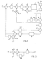
- the block diagram shown in Fig. 1 of an embodiment of the invention contains the input e for the input data, that is, the digital video signals, the number of digits z. B. is to be reduced from 8 to 4.
- the input data are fed to the first retarder v1, the output of which is located at the minuend input of the first subtractor s1, and the output of which reaches the minuend input of the second subtractor s2 via the second retarder v2.
- the input data in FIG. 1, which change in time with a clock signal are at the minuend input of the third subtractor s3, from the output of which they arrive at the input of the first delayer v1.
- the output of the second subtractor s2 is at the input of the quantizer q, the structure of which can be of the type described above, which in particular can be a read-only memory with a quantization table for 16 values. Its output is on the one hand via the code converter cw at the output for the data-reduced output signal rv and on the other hand directly at the input of the third delay v3.
- the essential basic idea of the invention lies in this direct connection of quantizer q and delay device v3, since the adder and the delimiter, which are in this connection in the arrangement described above, can be omitted and thus significant computing time can be saved in the time-critical loop.
- the output of the third delay v3 is also connected via the first 2- 1 multiplier m11 to the sub-frame input of the second subtractor s2.
- the output of the first adder A1 is connected via the first 2- 2 multiplier m21 to the subtrahend input of the first subtracter s1; it is also connected to its second input via the fourth delay v4 and the second 2- 1 multiplier m12 connected downstream thereof, and finally via the fifth delay v5 to the first input of the second adder a2.
- the output of the second adder a2 is via the vertical predictor vp and the sixth delay v6 connected downstream of it at the first input of the third adder a3, the output of which is connected to its second input via the seventh delay v7 and the third 2- 1 multiplier m13 connected downstream . Furthermore, this output is located directly at the subtrahend input of the third subtractor s3 and via the eighth delay v8 at the second input of the second adder a2.
- the respective delay time of the first to seventh delayers v1 ... v7 is equal to the period of the clock signal, but that of the eighth delayer v8 is four times as long.
- this consists in the signal flow direction of the ninth delay v9, its delay time to 5 periods of the clock signal is shorter than the duration of a line of the television picture, and further from the fourth adder A4, and the second 2- 2 multiplier m22.
- the output of the ninth delay v9 is connected to the second input of the fourth adder v4 via the tenth delay v10, the delay time of which is equal to the period of the clock signal.
- Parallel signal processing is also to be understood to mean that according to the so-called pipeline method, in which the individual digits of a digital word within the clock system formed by the clock signal are processed with a delay of at least one clock period compared to the other digits.
- the circuit arrangement according to the invention is not only suitable for implementation in the CMOS technology mentioned at the outset, but can also be implemented in N-channel MOS technology, the line width likewise being 2 ⁇ m.
Description
Die Erfindung betrifft eine Datenreduzierschaltung für die Stellenzahl von digitalen Videosignalen mit einem Differenz-Pulscodemodulator entsprechend dem Oberbegriff des Anspruchs 1. Eine derartige Datenreduzierschaltung ist in einem Aufsatz der Zeitschrift « Elektrisches Nachrichtenwesen ", Band 58, 1984, Seiten 447 bis 449 beschrieben. Nach Abschätzungen des Verfassers dieses Aufsatzes erlaubt die vorbeschriebene Anordnung eine Taktfrequenz von etwa 10 MHz und die Realisierung mittels einer einzigen integrierten Schaltung, wenn dafür eine 2-um-CMOS-Technik verwendet wird. Abgesehen von der Tatsache, daß eine CMOS-Herstelltechnik mit 2 um Linienbreite derzeit nur in Forschungs- und Entwicklungslaboratorien zur Verfügung steht und somit für die Massenfertigung von Halbleiterbauelementen noch nicht geeignet ist, ist die bei der vorbeschriebenen Anordnung maximal mögliche Taktfrequenz von etwa 10 MHz dann zu niedrig, wenn derartige Datenreduzierschaltungen in Schaltungen eingesetzt werden sollen, mit denen ein flimmerfreies Fernsehbild ermöglicht werden soll. In diesem Fall sind nämlich höhere Taktfrequenzen, die etwa 17 bis 20 MHz betragen, erforderlich.The invention relates to a data reduction circuit for the number of digits of digital video signals with a differential pulse code modulator according to the preamble of
Bei der vorbeschriebenen Anordnung sind in der die maximale Taktfrequenz begrenzenden zeitkritischen Schleife ein Subtrahierer, ein Addierer, ein Begrenzer und ein Quantisierer enthalten. Diese Schleife muß innerhalb einer Periode des Taktsignals die erforderlichen Berechnungen vornehmen, was bei entsprechend schnellen Addier-/Subtrahierstufen mittels der vorbeschriebenen Anordnung nur innerhalb etwa 100 ns erfolgen kann.In the arrangement described above, a subtractor, an adder, a limiter and a quantizer are contained in the time-critical loop which limits the maximum clock frequency. This loop must carry out the necessary calculations within a period of the clock signal, which can only be done within approximately 100 ns with correspondingly fast adding / subtracting stages by means of the arrangement described above.
Die Aufgabe der in den Ansprüchen gekennzeichneten Erfindung besteht daher darin, die zeitkritische schleife so auszugestalten, daß eine der beabsichtigten Arbeitsfrequenz von etwa 17 bis 20 MHz entsprechende kürzere Rechenzeit erreichbar ist. Dabei soll bewußt in Kauf genommen werden, daß sich die Gesamtschaltung gegenüber der vorbeschriebenen Anordnung komplizierter gestaltet und daß sie insgesamt betrachtet mehr Teilschaltungen enthält als die vorbeschriebene Schaltung. Der in der Aufgabenlösung liegende Vorteil einer im Vergleich zur vorbeschriebenen Anordnung etwa doppelt so schnellen Verarbeitungsgeschwindigkeit wird dadurch erreicht, daß die zeitkritische Schleife nur noch aus dem Quantisierer und einem Subtrahierer besteht, der Addierer und der Begrenzer also entfallen sind.The object of the invention characterized in the claims is therefore to design the time-critical loop so that a shorter computing time corresponding to the intended working frequency of about 17 to 20 MHz can be achieved. It should be consciously accepted that the overall circuit is more complicated than the arrangement described above and that, viewed as a whole, it contains more subcircuits than the circuit described above. The advantage of the task solution of a processing speed which is about twice as fast as that of the arrangement described above is achieved in that the time-critical loop consists only of the quantizer and a subtractor, so that the adder and the delimiter have been omitted.
Weitere Vorteile ergeben sich aus der weiteren Erläuterung der Erfindung anhand der Figuren der Zeichnung.
- Fig. 1 zeigt in Form eines Blockschaltbilds ein Ausführungsbeispiel der Erfindung, und
- Fig. 2 zeigt in Form eines Blockschaltbilds eine Ausgestaltung für eine Teilschaltung nach Fig. 1.
- Fig. 1 shows in the form of a block diagram an embodiment of the invention, and
- FIG. 2 shows in the form of a block diagram an embodiment for a subcircuit according to FIG. 1.
Das in Fig. 1 gezeigte Blockschaltbild eines Ausführungsbeispiels der Erfindung enthält den Eingang e für die Eingangsdaten, also die digitalen Videosignale, deren Stellenzahl z. B. von 8 auf 4 zu reduzieren ist. Die Eingangsdaten sind bei der vorbeschriebenen Anordnung dem ersten Verzögerer v1 zugeführt, dessen Ausgang am Minuend-Eingang des ersten Subtrahierers s1 liegt, von dessen Ausgang sie über den zweiten Verzögerer v2 an den Minuend-Eingang des zweiten Subtrahierers s2 gelangen. Nach einem Merkmal der Erfindung liegen in Fig. 1 die Eingangsdaten, die sich im Takt eines Taktsignals ändern, am Minuend-Eingang des dritten Subtrahierers s3, von dessen Ausgang sie an den Eingang des ersten Verzogerers v1 gelangen.The block diagram shown in Fig. 1 of an embodiment of the invention contains the input e for the input data, that is, the digital video signals, the number of digits z. B. is to be reduced from 8 to 4. In the arrangement described above, the input data are fed to the first retarder v1, the output of which is located at the minuend input of the first subtractor s1, and the output of which reaches the minuend input of the second subtractor s2 via the second retarder v2. According to one feature of the invention, the input data in FIG. 1, which change in time with a clock signal, are at the minuend input of the third subtractor s3, from the output of which they arrive at the input of the first delayer v1.
Der Ausgang des zweiten Subtrahierers s2 liegt am Eingang des Quantisierers q, dessen Aufbau von vorbeschriebener Art sein kann, der also insbesondere ein Festwertspeicher mit Quantisiertabelle für 16 Werte sein kann. Sein Ausgang liegt einerseits über den Codewandler cw am Ausgang für das datenreduzierte Ausgangssignal rv und andererseits direkt am Eingang des dritten Verzögerers v3. In dieser direkten Verbindung von Quantisierer q und Verzögerer v3 liegt der wesentliche Grundgedanke der Erfindung, da dadurch der Addierer und der Begrenzer, die bei der vorbeschriebenen Anordnung in dieser Verbindung liegen, weggelassen werden können und somit in der zeitkritischen Schleife wesentliche Rechenzeit eingespart werden kann. Der Ausgang des dritten Verzögerers v3 ist ferner über den ersten 2-1-Multiplizierer m11 mit dem Subfrahend-Eingang des zweiten Subtrahierers s2 verbunden.The output of the second subtractor s2 is at the input of the quantizer q, the structure of which can be of the type described above, which in particular can be a read-only memory with a quantization table for 16 values. Its output is on the one hand via the code converter cw at the output for the data-reduced output signal rv and on the other hand directly at the input of the third delay v3. The essential basic idea of the invention lies in this direct connection of quantizer q and delay device v3, since the adder and the delimiter, which are in this connection in the arrangement described above, can be omitted and thus significant computing time can be saved in the time-critical loop. The output of the third delay v3 is also connected via the first 2- 1 multiplier m11 to the sub-frame input of the second subtractor s2.
Der Ausgang des ersten Addierers a1 ist über den ersten 2-2-Multiplizierer m21 mit dem Subtrahend-Eingang des ersten Subtrahierers s1 verbunden ; ferner liegt er über den vierten Verzögerer v4 und den diesem nachgeschalteten zweiten 2-1-Multiplizierer m12 an seinem zweiten Eingang und schließlich über den fünften Verzögerer v5 am ersten Eingang des zweiten Addierers a2.The output of the first adder A1 is connected via the first 2- 2 multiplier m21 to the subtrahend input of the first subtracter s1; it is also connected to its second input via the fourth delay v4 and the second 2- 1 multiplier m12 connected downstream thereof, and finally via the fifth delay v5 to the first input of the second adder a2.
Der Ausgang des zweiten Addierers a2 liegt über den Vertikalprädiktor vp und den diesem nachgeschalteten sechsten Verzögerer v6 am ersten Eingang des dritten Addierers a3, dessen Ausgang über den siebten Verzögerer v7 und den diesem nachgeschalteten dritten 2-1-Multiplizierer m13 mit seinem zweiten Eingang verbunden ist. Ferner liegt dieser Ausgang direkt am Subtrahend-Eingang des dritten Subtrahierers s3 und über den achten Verzögerer v8 am zweiten Eingang des zweiten Addierers a2.The output of the second adder a2 is via the vertical predictor vp and the sixth delay v6 connected downstream of it at the first input of the third adder a3, the output of which is connected to its second input via the seventh delay v7 and the third 2- 1 multiplier m13 connected downstream . Furthermore, this output is located directly at the subtrahend input of the third subtractor s3 and via the eighth delay v8 at the second input of the second adder a2.
Die jeweilige Verzögerungszeit des ersten bis siebten Verzögerers v1 ... v7 ist gleich der Periodendauer des Taktsignals, die des achten Verzögerers v8 jedoch viermal so groß.The respective delay time of the first to seventh delayers v1 ... v7 is equal to the period of the clock signal, but that of the eighth delayer v8 is four times as long.
Nach dem in Fig. 2 gezeigten Ausführungsbeispiel für den Vertikalprädiktor vp nach Fig. 1 besteht dieser in Signalflußrichtung aus dem neunten Verzögerer v9, dessen Verzögerungszeit um 5 Periodendauern des Taktsignals kürzer ist als die Dauer einer Zeile des Fernsehbilds, und ferner aus dem vierten Addierer a4 sowie dem zweiten 2-2-Multiplizierer m22. Dabei ist der Ausgang des neunten Verzögerers v9 uber den zehnten Verzögerer v10, dessen Verzögerungszeit gleich der Periodendauer des Taktsignals ist, mit dem zweiten Eingang des vierten Addierers v4 verbunden.According to the exemplary embodiment shown in FIG. 2 for the vertical predictor vp according to FIG. 1, this consists in the signal flow direction of the ninth delay v9, its delay time to 5 periods of the clock signal is shorter than the duration of a line of the television picture, and further from the fourth adder A4, and the second 2- 2 multiplier m22. The output of the ninth delay v9 is connected to the second input of the fourth adder v4 via the tenth delay v10, the delay time of which is equal to the period of the clock signal.
Obwohl in den Figuren der Zeichnung die signalführenden Leitungen zweischen den einzelnen Teilschaltungen lediglich als einfache Verbindungsleitungen gezeigt sind, symbolisieren diese jedoch Busse, da die einzelnen Teilschaltungen solche zur parallelen Verarbeitung von Datenwörtern sind, was sich aus der eingangs erwähnten Arbeitsgeschwindigkeit der Datenreduzierschaltung nach der Erfindung ergibt. Unter paralleler Signalverarbeitung soll dabei auch eine solche nach dem sogenannten Pipeline-Verfahren verstanden werden, bei dem die einzelnen Stellen eines Digitalworts innerhalb des vom Taktsignal gebildeten Taktsystems um mindestens eine Taktperiode verzögert gegenüber den anderen Stellen verarbeitet werden.Although in the figures of the drawing the signal-carrying lines between the individual subcircuits are only shown as simple connecting lines, these symbolize buses, however, since the individual subcircuits are those for parallel processing of data words, which results from the operating speed of the data reduction circuit according to the invention mentioned at the outset . Parallel signal processing is also to be understood to mean that according to the so-called pipeline method, in which the individual digits of a digital word within the clock system formed by the clock signal are processed with a delay of at least one clock period compared to the other digits.
Die Schaltungsanordnung nach der Erfindung eignet sich nicht nur zur Realisierung in der eingangs erwähnten CMOS-Technik, sondern kann auch in N-Kanal-MOS-Technik realisiert werden, wobei deren Linienbreite ebenfalls 2 um beträgt.The circuit arrangement according to the invention is not only suitable for implementation in the CMOS technology mentioned at the outset, but can also be implemented in N-channel MOS technology, the line width likewise being 2 μm.
Claims (2)
Priority Applications (5)
| Application Number | Priority Date | Filing Date | Title |
|---|---|---|---|
| DE8585104051T DE3571731D1 (en) | 1985-04-03 | 1985-04-03 | Circuit for compressing data for digital video signals with a difference pulse code modulator |
| EP85104051A EP0197165B1 (en) | 1985-04-03 | 1985-04-03 | Circuit for compressing data for digital video signals with a difference pulse code modulator |
| CN86101610.6A CN1004533B (en) | 1985-04-03 | 1986-03-13 | Data reduction circuit with a differential pulse code modulator |
| US06/847,646 US4713828A (en) | 1985-04-03 | 1986-04-03 | Data reduction circuit |
| JP61075674A JPS61232725A (en) | 1985-04-03 | 1986-04-03 | Data compression circuit |
Applications Claiming Priority (1)
| Application Number | Priority Date | Filing Date | Title |
|---|---|---|---|
| EP85104051A EP0197165B1 (en) | 1985-04-03 | 1985-04-03 | Circuit for compressing data for digital video signals with a difference pulse code modulator |
Publications (2)
| Publication Number | Publication Date |
|---|---|
| EP0197165A1 EP0197165A1 (en) | 1986-10-15 |
| EP0197165B1 true EP0197165B1 (en) | 1989-07-19 |
Family
ID=8193423
Family Applications (1)
| Application Number | Title | Priority Date | Filing Date |
|---|---|---|---|
| EP85104051A Expired EP0197165B1 (en) | 1985-04-03 | 1985-04-03 | Circuit for compressing data for digital video signals with a difference pulse code modulator |
Country Status (5)
| Country | Link |
|---|---|
| US (1) | US4713828A (en) |
| EP (1) | EP0197165B1 (en) |
| JP (1) | JPS61232725A (en) |
| CN (1) | CN1004533B (en) |
| DE (1) | DE3571731D1 (en) |
Families Citing this family (6)
| Publication number | Priority date | Publication date | Assignee | Title |
|---|---|---|---|---|
| DE3417139A1 (en) * | 1984-05-09 | 1985-11-14 | Standard Elektrik Lorenz Ag, 7000 Stuttgart | Digital DPCM coder/decoder for high processing speeds, particularly for television picture signals |
| FR2602936B1 (en) * | 1986-08-13 | 1988-12-02 | Trt Telecom Radio Electr | DIFFERENTIAL MODULATION BY CODED PULSE CODING DEVICE, ASSOCIATED DECODING DEVICE, AND TRANSMISSION SYSTEM COMPRISING AT LEAST ONE SUCH CODING OR DECODING DEVICE |
| EP0278012A1 (en) * | 1987-02-06 | 1988-08-17 | Deutsche ITT Industries GmbH | Circuit for controlling a memory arrangement |
| US5357278A (en) * | 1993-01-14 | 1994-10-18 | Sony Electronics, Inc. | Integrated linear/non-linear static and controllable dynamic companding |
| US7372692B2 (en) * | 2006-10-09 | 2008-05-13 | Eaton Corporation | Electrical enclosure and interior assembly therefor |
| SG189549A1 (en) * | 2010-11-02 | 2013-06-28 | I Ces Innovative Compression Engineering Solutions | Method for compressing digital values of image, audio and/or video files |
Family Cites Families (6)
| Publication number | Priority date | Publication date | Assignee | Title |
|---|---|---|---|---|
| CA1085044A (en) * | 1975-04-03 | 1980-09-02 | Yukihiko Iijima | Composite feedback predictive code communication system for a color tv signal including a carrier chrominance signal |
| FR2463549A1 (en) * | 1979-08-10 | 1981-02-20 | Telecommunications Sa | DEVICE FOR REDUCING THE DIGITAL RATE OF CODE INFORMATION |
| US4255763A (en) * | 1979-12-26 | 1981-03-10 | Bell Telephone Laboratories, Incorporated | Technique for reducing transmission error propagation in an adaptively predicted DPCM video encoder |
| US4460923A (en) * | 1981-06-01 | 1984-07-17 | Nippon Electric Co., Ltd. | Predictive coding system for television signals |
| JPS58197984A (en) * | 1982-05-14 | 1983-11-17 | Nec Corp | Adaptive forecasting encoding device of television signal |
| DE3232516A1 (en) * | 1982-09-01 | 1984-03-01 | Siemens AG, 1000 Berlin und 8000 München | FAST DPCM ENCODER |
-
1985
- 1985-04-03 DE DE8585104051T patent/DE3571731D1/en not_active Expired
- 1985-04-03 EP EP85104051A patent/EP0197165B1/en not_active Expired
-
1986
- 1986-03-13 CN CN86101610.6A patent/CN1004533B/en not_active Expired
- 1986-04-03 US US06/847,646 patent/US4713828A/en not_active Expired - Fee Related
- 1986-04-03 JP JP61075674A patent/JPS61232725A/en active Pending
Also Published As
| Publication number | Publication date |
|---|---|
| JPS61232725A (en) | 1986-10-17 |
| CN1004533B (en) | 1989-06-14 |
| DE3571731D1 (en) | 1989-08-24 |
| CN86101610A (en) | 1986-10-01 |
| US4713828A (en) | 1987-12-15 |
| EP0197165A1 (en) | 1986-10-15 |
Similar Documents
| Publication | Publication Date | Title |
|---|---|---|
| DE4302898C2 (en) | Arithmetic arithmetic unit with accumulation function | |
| DE3044208C2 (en) | Interpolator for increasing the word speed of a digital signal | |
| DE3124924C2 (en) | ||
| DE69435034T2 (en) | METHOD OF DEVICE FOR CARRYING OUT A QUICK HADAMARD TRANSFORM | |
| DE69432587T2 (en) | DELAY LINE SEPARATOR FOR DATA BUS | |
| DE2605724C2 (en) | Digital-to-analog converter for PCM-coded digital signals | |
| EP0197165B1 (en) | Circuit for compressing data for digital video signals with a difference pulse code modulator | |
| EP0181953A1 (en) | Interpolator for digital signals | |
| EP0660246A2 (en) | Signal processor | |
| DE2900844C2 (en) | ||
| EP0242413B1 (en) | Data reducing circuit with a differential pulse code modulator for video signals | |
| DE3334541A1 (en) | DIGITAL SIGNAL FILTER DEVICE | |
| DE69636352T2 (en) | Hierarchical coding apparatus and method with memory for a digital image signal | |
| DE3822324A1 (en) | DEVICE FOR DISASSEMBLING THE PRIORITY VALUE | |
| DE4022387C2 (en) | ||
| EP0346750B1 (en) | Device for dpcm coding at a high data rate | |
| EP0221617B1 (en) | Low-pass digital filter | |
| EP0135599B1 (en) | Digital filter integrated circuit for the luminance channel of a colour television receiver | |
| DE2349905A1 (en) | DEVICE FOR SIGNAL TRANSFER BETWEEN SYSTEMS WITH NON-SYNCHRONOUS TIME CONTROL | |
| DE3621446A1 (en) | DEVICE FOR DIGITAL PROCESSING OF CONTINUOUS BIT FLOWS | |
| EP0305708A2 (en) | Digital decimating filter | |
| DE3308703A1 (en) | CONFERENCE CALLS | |
| DE3490580C2 (en) | ||
| EP0307512B1 (en) | Digital data slicing circuit for teletext signals | |
| EP0192788B1 (en) | Integrated digital circuit section for frequency demodulation |
Legal Events
| Date | Code | Title | Description |
|---|---|---|---|
| PUAI | Public reference made under article 153(3) epc to a published international application that has entered the european phase |
Free format text: ORIGINAL CODE: 0009012 |
|
| 17P | Request for examination filed |
Effective date: 19860328 |
|
| AK | Designated contracting states |
Kind code of ref document: A1 Designated state(s): DE FR GB IT NL |
|
| 17Q | First examination report despatched |
Effective date: 19880920 |
|
| GRAA | (expected) grant |
Free format text: ORIGINAL CODE: 0009210 |
|
| AK | Designated contracting states |
Kind code of ref document: B1 Designated state(s): DE FR GB IT NL |
|
| GBT | Gb: translation of ep patent filed (gb section 77(6)(a)/1977) | ||
| REF | Corresponds to: |
Ref document number: 3571731 Country of ref document: DE Date of ref document: 19890824 |
|
| ET | Fr: translation filed | ||
| ITF | It: translation for a ep patent filed |
Owner name: BUGNION S.P.A. |
|
| PLBE | No opposition filed within time limit |
Free format text: ORIGINAL CODE: 0009261 |
|
| STAA | Information on the status of an ep patent application or granted ep patent |
Free format text: STATUS: NO OPPOSITION FILED WITHIN TIME LIMIT |
|
| 26N | No opposition filed | ||
| ITTA | It: last paid annual fee | ||
| PGFP | Annual fee paid to national office [announced via postgrant information from national office to epo] |
Ref country code: GB Payment date: 19930324 Year of fee payment: 9 |
|
| PG25 | Lapsed in a contracting state [announced via postgrant information from national office to epo] |
Ref country code: GB Effective date: 19940403 |
|
| GBPC | Gb: european patent ceased through non-payment of renewal fee |
Effective date: 19940403 |
|
| PGFP | Annual fee paid to national office [announced via postgrant information from national office to epo] |
Ref country code: FR Payment date: 19950313 Year of fee payment: 11 |
|
| PGFP | Annual fee paid to national office [announced via postgrant information from national office to epo] |
Ref country code: DE Payment date: 19950421 Year of fee payment: 11 |
|
| PGFP | Annual fee paid to national office [announced via postgrant information from national office to epo] |
Ref country code: NL Payment date: 19950430 Year of fee payment: 11 |
|
| PG25 | Lapsed in a contracting state [announced via postgrant information from national office to epo] |
Ref country code: NL Effective date: 19961101 |
|
| PG25 | Lapsed in a contracting state [announced via postgrant information from national office to epo] |
Ref country code: FR Effective date: 19961227 |
|
| PG25 | Lapsed in a contracting state [announced via postgrant information from national office to epo] |
Ref country code: DE Effective date: 19970101 |
|
| NLV4 | Nl: lapsed or anulled due to non-payment of the annual fee |
Effective date: 19961101 |
|
| REG | Reference to a national code |
Ref country code: FR Ref legal event code: ST |