EP0660246A2 - Signal processor - Google Patents
Signal processor Download PDFInfo
- Publication number
- EP0660246A2 EP0660246A2 EP94203670A EP94203670A EP0660246A2 EP 0660246 A2 EP0660246 A2 EP 0660246A2 EP 94203670 A EP94203670 A EP 94203670A EP 94203670 A EP94203670 A EP 94203670A EP 0660246 A2 EP0660246 A2 EP 0660246A2
- Authority
- EP
- European Patent Office
- Prior art keywords
- data
- data processing
- processing unit
- signal processor
- arithmetic
- Prior art date
- Legal status (The legal status is an assumption and is not a legal conclusion. Google has not performed a legal analysis and makes no representation as to the accuracy of the status listed.)
- Withdrawn
Links
Images

Classifications
-
- G—PHYSICS
- G06—COMPUTING; CALCULATING OR COUNTING
- G06F—ELECTRIC DIGITAL DATA PROCESSING
- G06F7/00—Methods or arrangements for processing data by operating upon the order or content of the data handled
- G06F7/06—Arrangements for sorting, selecting, merging, or comparing data on individual record carriers
-
- G—PHYSICS
- G06—COMPUTING; CALCULATING OR COUNTING
- G06F—ELECTRIC DIGITAL DATA PROCESSING
- G06F17/00—Digital computing or data processing equipment or methods, specially adapted for specific functions
- G06F17/10—Complex mathematical operations
-
- G—PHYSICS
- G06—COMPUTING; CALCULATING OR COUNTING
- G06F—ELECTRIC DIGITAL DATA PROCESSING
- G06F15/00—Digital computers in general; Data processing equipment in general
- G06F15/76—Architectures of general purpose stored program computers
- G06F15/78—Architectures of general purpose stored program computers comprising a single central processing unit
- G06F15/7807—System on chip, i.e. computer system on a single chip; System in package, i.e. computer system on one or more chips in a single package
- G06F15/7817—Specially adapted for signal processing, e.g. Harvard architectures
-
- G—PHYSICS
- G06—COMPUTING; CALCULATING OR COUNTING
- G06F—ELECTRIC DIGITAL DATA PROCESSING
- G06F7/00—Methods or arrangements for processing data by operating upon the order or content of the data handled
- G06F7/38—Methods or arrangements for performing computations using exclusively denominational number representation, e.g. using binary, ternary, decimal representation
- G06F7/48—Methods or arrangements for performing computations using exclusively denominational number representation, e.g. using binary, ternary, decimal representation using non-contact-making devices, e.g. tube, solid state device; using unspecified devices
- G06F7/544—Methods or arrangements for performing computations using exclusively denominational number representation, e.g. using binary, ternary, decimal representation using non-contact-making devices, e.g. tube, solid state device; using unspecified devices for evaluating functions by calculation
- G06F7/5443—Sum of products
-
- H—ELECTRICITY
- H04—ELECTRIC COMMUNICATION TECHNIQUE
- H04B—TRANSMISSION
- H04B1/00—Details of transmission systems, not covered by a single one of groups H04B3/00 - H04B13/00; Details of transmission systems not characterised by the medium used for transmission
- H04B1/38—Transceivers, i.e. devices in which transmitter and receiver form a structural unit and in which at least one part is used for functions of transmitting and receiving
- H04B1/40—Circuits
Definitions
- the invention relates to a signal processor with a data processing unit with means for processing data by arithmetic or logical operations.
- the invention also relates to a radio with a signal processor with a data processing unit with means for processing data by arithmetic or logical operations.
- Signal processors are usually used for this. Another possible technical solution is the use of chips specially developed for this application. Signal processors are special microcomputers for real-time applications. Further areas of application for signal processors are, for example, audio, video, medical, automotive technology.
- a signal processor of the type mentioned at the beginning is known from the essay "Digital Signal Processors, Part One: Processors for Special Tasks" by M. Kappelan and H. Mucke, Funkschau 16/1993, pages 66 to 69.
- the processor has a data processing unit which is coupled to two data memories via two data buses. An addressing unit uses two address buses to address the respective data stored in the data memories, which are fed to the data processing unit via the two data buses.
- the data processing unit consists of a multiplier arranged on the input side, an adder and an accumulator. Since the multiplier receives two data to be multiplied in parallel via the two data buses, multiplication and addition can be carried out within one command cycle.
- Some signal processors have data processing units which are able to multiply two received data in one command cycle, to form the sum of the product obtained and the old accumulator content and to overwrite the accumulator with this sum. With other signal processors, only a multiplication result from a previous command cycle stored in a buffer can be used for the addition. An initialization of the data processing unit of such signal processors requires an additional command cycle because of the additional buffer. Processing of data by the data processing unit is carried out by "pipeline” processing, in which received data in several stages, i.e. Command cycles to be processed. For this purpose, the data processing unit in two-stage "pipeline” processing has two receive registers and an accumulator as the output register. With certain signal processors, an additional buffer is required, as described above, so that a three-stage "pipeline” processing results.
- the calculation of a product sum or a scalar product from two data vectors is a typical application of a signal processor, for example in the calculation of auto-correlation functions, cross-correlation functions or in digital signal processing with FIR filters.
- a signal processor for example in the calculation of auto-correlation functions, cross-correlation functions or in digital signal processing with FIR filters.
- the computing speed of signal processors according to the prior art may not be sufficient.
- Increasing the computing speed by connecting further data processing units in parallel, to which data are fed via additional data buses, is technically complex and costly.
- the invention is therefore based on the object of providing a signal processor whose computing speed is increased with little additional technical outlay.
- the object is achieved in a signal processor of the type mentioned at the outset in that at least one further data processing unit working in parallel with the data processing unit is provided with means for processing data derived from the data supplied to the data processing unit.
- Such a signal processor has, compared to a signal processor with only one data processing unit, an increased computing speed for all those cases in which the data supplied to the first data processing device or intermediate or output values of the first data processing unit derived therefrom are evaluated by at least one further data processing unit working in parallel with the first data processing unit become.
- each further data processing unit working in this way is coupled to the first data processing unit.
- input values, ie supplied data, of the first data processing unit or intermediate or output values of the first data processing unit are passed on to a second data processing unit, the input, intermediate or output values of which are transmitted to a third data processing unit.
- the fourth data processing unit is supplied with input, intermediate or output values from the second or third data processing unit.
- any number of others can be parallel Arrange working data processing units.
- the additional technical outlay is essentially limited to the circuitry implementation of the further data processing units.
- the additional space requirement on a chip on which the signal processor is implemented is small in comparison to the implementation of additional data buses.
- the arithmetic operations performed in the data processing units include multiplication and division as well as addition and subtraction. Examples of logical operations are the AND, NOT, OR or exclusive OR operation.
- the invention is designed in such a way that the data supplied to the means of the first data processing unit is supplied to the means of at least one further data processing unit in the same and / or in a different command cycle.
- identical data vectors are used to calculate result values by the data processing units, the components of which are identical to the data to be processed.
- Several result values can thus be determined in a number of command cycles which corresponds to the number of components of the respective data vector. If components of a data vector which is processed by the first data processing unit to determine a result value are only partially required to determine a further result value and the location of the same data in the corresponding data vectors is offset, the same data is processed in different command cycles by the Data processing units useful to enable parallel calculation of result values by several data processing units. A necessary time offset between the data is easily generated by temporarily storing the data.
- a first data bus is coupled to the data processing means of the first and at least one further data processing unit
- a second data bus is coupled to the data processing means of the first data processing unit and via one in each each additional data processing unit arranged storage means for intermediate storage of data is coupled with the data processing means of the respective further data processing unit and that in the case of several further data processing units all storage means are connected in series.
- the data buses serve for the simultaneous transmission of data to a multiplier arranged in the data processing unit, which multiplier can thus form the product of two data within one command cycle.
- the invention is advantageously applicable to these signal processors and increases their computing speed without the need for additional data buses.
- the expansion of a signal processor is limited to arranging at least one further data processing unit on the chip of such a signal processor, which is technically easy to implement.
- the first data bus delivers data to the first and at least one further data processing unit, which process the data in parallel by the means provided for this purpose.
- the second data bus supplies data to the data processing means of the first data processing unit and via storage means for temporarily storing data to the means of each further data processing unit. If more than one further data processing device is provided, all of the storage means for temporarily storing data are connected in series. In this way it follows that the data transmitted over the second data bus are processed by the data processing units at different times, ie in different command cycles.
- Typical applications of signal processors are, for example, the calculation of autocorrelation functions, cross-correlation functions and digital filtering with FIR filters. In these applications it is necessary to form scalar products of data vectors.
- the data processing units are thus provided for the formation of products of the supplied data and for the summation of the products.
- the means for processing data each have a multiplier arranged on the input side, the output of which is coupled to a first input of an arithmetic / logic unit and that the arithmetic / logic unit has one has the output of an accumulator coupled second input and an output coupled to the input of the accumulator.
- Data received on the input side are first multiplied by the respective multiplier and then summed up with the aid of the arithmetic / logic unit and the accumulator.
- the arithmetic / logic unit is used as an adder in the present application.
- the arithmetic / logical unit is at least the first data processing unit also intended for other arithmetic or logical functions.
- the signal processor shown in FIG. 1 has a bus system 1, via which a number of function blocks are coupled to one another.
- the bus system 1 contains buses for the transmission of data, addresses and control signals.
- the bus system 1 thus has, among other things, a data bus system and a program bus, which are not shown in detail.
- An addressing unit 2 supplies addresses to a memory unit 3, so that associated memory contents are read out.
- the storage unit 3 generally exists from a ROM and / or a RAM.
- first and second data processing units 4 and 5 are provided, which are used to process the data read out from the storage unit 3.
- the second data processing unit 5 is not directly connected on the input side to the data bus system of the bus system 1, but receives data via the first data processing unit 4.
- a program storage unit 6 is connected via the program bus to the units connected to the bus system 1.
- a control unit 8 is coupled via control lines to the units connected to the bus system 1. The control unit 8 controls the program sequence and coordinates the access of the units 2 to 7 to the bus system 1.
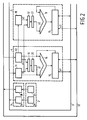
- FIG. 2 shows part of the signal processor shown in FIG. 1 in more detail.
- the storage unit 3 has a first data store 3a and a second data store 3b.
- the first data memory 3a is coupled to a first data bus 9 and the second data memory 3b is coupled to a second data bus 10.
- a first and second addressing block 2a and 2b, which are arranged in the addressing unit 2, are used to deliver addresses to the first data store 3a and the second data store 3b.
- a first register 11 is provided on the input side of the first data processing unit 4 and receives data from the first data bus 9.
- a second register 12 receives data from the second data bus 10. Both registers 11 and 12 serve to buffer the received data.
- the one from the registers 11 and 12 received data are multiplied by a multiplier 13, which supplies a product p1 formed by it via a register 20 to a first input of an arithmetic / logic unit 14.
- the memory content of an accumulator 15, which is overwritten with the output value of the arithmetic / logic unit 14, is fed to a second input of the arithmetic / logic unit 14, which functions as an adder or a subtractor.
- the signal processor can also be programmed so that the arithmetic / logic unit 14 performs other arithmetic or logic operations. Furthermore, instead of the output of the multiplier 13, the first input of the arithmetic / logic unit 14 can also be supplied with data directly from the register 11. A direct connection of the output of the register 12 to the second input of the arithmetic / logic unit 14 instead of to an input of the multiplier 13 is also possible.
- the output of the accumulator 15 is coupled to the storage unit 3 either via the first or the second data bus 9 or 10.
- the data buses 9 and 10 are also provided for data transport from the storage unit 3 to the accumulator 15, for example in order to initialize the accumulator 15.
- the second data processing unit 5 has a third register 16, which receives the data temporarily stored in the second register 12, stores them temporarily and supplies them to a multiplier 17.
- the multiplier 17 also receives the data buffered in the first register 11.
- the data present at the outputs of the first register 11 and the third register 16 are multiplied and the resulting product p2 is passed via a register 21 to a first input of an arithmetic / logic unit 18. Its second input is coupled to an output of an accumulator 19, which is overwritten with the output values of the arithmetic / logic unit 18.
- the arithmetic / logic unit 18 is a simple adder / subtractor in the present case. It can, but does not have to be able to implement any other functions.
- the accumulator 19 is coupled to the storage unit 3 in a manner analogous to the accumulator 15 via the first or the second data bus 9 or 10.
- the present signal processor is particularly suitable for calculating a set of n scalar products of the form a (j) and b (j + i) are data that are components of two data vectors and i have dimension m interpreted.
- the data vector is used identically to calculate all dot products c (i).
- the number of different data vectors In the present case, i corresponds to the number n of scalar products c (i) to be calculated.
- the components of the data vectors used to calculate the dot products c (i) i are partially identical as can be seen from the formula given.
- the values d (i) represent the initial values with which the associated two accumulators 15 and 19 are initialized at the start of a calculation of two scalar products c (i) and c (i-1) (in particular, as in the present exemplary embodiment, with the value zero ).
- Such scalar products are formed in particular in the calculation of autocorrelation functions, cross-correlation functions and in digital filtering using FIR filters.
- the table below explains the parallel calculation of two scalar products using the example of calculating the scalar products c (0) and c (1).
- the lines of the table numbered from 1 to m + 3 with the aid of the first column serve to explain m + 3 required command cycles of the signal processor.
- x1 and x2 represent the respective output value or memory content of registers 12 and 16.
- y corresponds to the respective value present at the output of register 11.
- the products supplied by multipliers 13 and 17 are in the columns under p1 and p2.
- a1 and a2 are the memory contents of the accumulators 15 and 19.
- the signal processor explained in more detail by FIG. 2 processes data according to the principle of the so-called "pipeline” processing.
- a three-stage "pipeline” processing used ie the data processing units have three stages. The three stages are traversed by the data transmitted via the data buses 9 and 10 in three successive command cycles.
- data is loaded into registers 11, 12 and 16 arranged on the input side.
- products p1 and p2 which are temporarily stored in registers 20 and 21, are simultaneously formed from data stored in registers 11, 12 and 16 in the previous command cycle with the aid of multipliers 13 and 17.
- the products p1 and p2 of the products temporarily stored in the register 20 and 21 in the previous command cycle are summed up to the contents of the accumulators 15 and 19.
- the second stage of the "pipeline" processing with a buffering in the registers 20 and 21 as in the present exemplary embodiment is necessary for all signal processors whose data processing units are not able to multiply and sum up the resulting product to the content within a command cycle the accumulators 15 and 19 to perform. In the case of signal processors that are capable of this, the second stage or the intermediate storage in the registers 20 and 21 can be omitted.
- the registers 11 and 12 are supplied with data stored in the data memories 3a and 3b via the data buses 9 and 10.
- the addressing unit 2 supplies the appropriate addresses to the data memories 3a and 3b in a program-controlled manner via two address buses.
- an initialization is carried out in the first three command cycles.
- the data memory 3b transfers the value b (0) to the register 12.
- the value b (0) is transferred to the register 16 of the second data processing unit 5.
- the data a (0) and b (1) are read into the registers 11 and 12 of the first data processing unit 4 from the data memories 3a and 3b.
- the memory content of register 16 is then overwritten with the memory content of register 12. Further data a (1) and b (2) can now be read into registers 11 and 12.
- Initialization is completed with the first three command cycles described.
- the registers 11 and 16 have indefinite memory contents in the first instruction cycle.
- the values p1 and p2 stored in the registers 20 and 21 are indefinite in the first and second instruction cycle.
- the memory content of the accumulators 15 and 19 is set to d (1) and d (0) during initialization, i.e. in this example set to zero.
- the products p1 and p2 determined in the preceding command cycle by the multipliers 13 and 17 are summed up for the first time on the accumulators 15 and 19.
- the further processing of data is carried out analogously to the function of the signal processor described above and can be seen from the table in Remove connection with Fig. 2.
- the instruction cycle m + 3 the memory contents a1 and a2 of the accumulators 15 and 19 are equal to the scalar products c (1) and c (0). These are transferred to the memory unit 3 via the data buses 9 and 10 and stored there for further processing.
- the parallel calculation of the next two scalar products c (2) and c (3) can then be carried out.
- the signal processor for the signal processor compared to a signal processor with only one data processing unit is doubled in the calculation of scalar products of the type mentioned.
- an increase in the calculation speed can always be achieved when the calculation data necessary for a scalar product are also at least partially required for the calculation of one or more other scalar products.
- further data processing units can be arranged in the signal processor, which are constructed like the data processing unit 5. All registers of these further data processing units arranged on the input side are connected in series with registers 12 and 16. The output of the register 11 is connected to an input of the multipliers of all data processing units.
- the calculated scalar products of the additional data processing units are likewise transmitted to the storage unit 3 via the data bus 9 or the data bus 10 and stored there for later processing.
- no additional data buses are necessary for the second data processing unit 5 and any further data processing unit, so that the additional circuitry outlay is low.
- Registers 11 and 12 or 20 and 21 only serve to ensure error-free "pipeline” processing. With sufficiently fast signal processors, a two-stage "pipeline” processing can take place, so that the registers 20 and 21 are superfluous.
- the block diagram of a digital radio telephone shown in FIG. 3 contains a transmission and reception path.
- the voice signals received by a microphone 30 are converted into binary-coded data words via an analog-digital converter 31. These data words are fed to a signal processor 32.
- a signal processor 32 For the various functions which the signal processor 32 performs, blocks 33 to 39 are shown in FIG. 3 in the signal processor 32.
- speech coding is carried out in block 33, then channel coding in block 34 and then encryption in block 35.
- These encrypted data words are GMSK-modulated in a modulator 40. This is connected to an output of the signal processor 32.
- the modulated digital signals are then converted into analog modulated signals in a digital-to-analog converter 41. These modulated analog signals are fed to a transmission circuit 42 which generates radio signals which are emitted via an antenna 43.
- the path described so far represents the transmission path of the digital radio telephone.
- Analog radio signals received by an antenna 44 are processed in a receiving circuit 45 and analog modulated signals are fed to an analog-to-digital converter 46.
- the digitally modulated signals output by the analog-to-digital converter are in a demodulator 47 demodulated and fed to the signal processor 32.
- Block 39 in signal processor 32 is intended to show the subsequent equalization of the demodulated signals.
- a decryption function is then carried out, which is symbolized by block 38.
- the signal processor 32 forwards digital data words to a digital-to-analog converter 48, which outputs the analog voice signals to a loudspeaker 49.
- the signal processor 32 can be used not only in a mobile station of a mobile radio system as a radio telephone, but also in a base station of such a system.
- the structure of a signal processor explained in FIG. 2 is furthermore not limited to signal processors.
- this structure can also be implemented on microcomputers or chips specially developed for radio devices in a mobile radio system (mobile and base stations).
Abstract
Description
Die Erfindung betrifft einen Signalprozessor mit einer Datenverarbeitungseinheit mit Mitteln zur Verarbeitung von Daten durch arithmetische oder logische Operationen. Die Erfindung betrifft auch ein Funkgerät mit einem Signalprozessor mit einer Datenverarbeitungseinheit mit Mitteln zur Verarbeitung von Daten durch arithmetische oder logische Operationen.The invention relates to a signal processor with a data processing unit with means for processing data by arithmetic or logical operations. The invention also relates to a radio with a signal processor with a data processing unit with means for processing data by arithmetic or logical operations.
Funkgeräte für Mobilfunk müssen in der Lage sein, komplexe Algorithmen zur Sprachverarbeitung in Echtzeit umzusetzen. In der Regel werden dazu Signalprozessoren verwendet. Ein Einsatz von speziellen für diesen Anwendungsfall entwikkelten Chips ist eine andere mögliche technische Lösung. Signalprozessoren sind spezielle Mikrocomputer für Echtzeitanwendungen. Weitere Anwendungsgebiete von Signalprozessoren sind beispielsweise Audio-, Video-, Medizin-, Kraftfahrzeug-Technik. Aus dem Aufsatz "Digitale Signalprozessoren, erster Teil: Prozessoren für besondere Aufgaben" von M. Kappelan und H. Mucke, Funkschau 16/1993, Seiten 66 bis 69, ist ein Signalprozessor der eingangs genannten Art bekannt. Der Prozessor weist eine Datenverarbeitungseinheit auf, die über zwei Datenbusse mit zwei Datenspeichern gekoppelt ist. Eine Adressierungseinheit adressiert über zwei Adressbusse die jeweiligen in den Datenspeichern abgelegten Daten, die über die beiden Datenbusse der Datenverarbeitungseinheit zugeführt werden. Die Datenverarbeitungseinheit besteht aus einem eingangsseitig angeordneten Multiplizierer, einem Addierer und einem Akkumulator. Da der Multiplizierer zwei zu multiplizierende Daten parallel über die beiden Datenbusse empfängt, kann innerhalb eines Befehlszyklus eine Multiplikation und eine Addition durchgeführt werden.Mobile radios must be able to implement complex speech processing algorithms in real time. Signal processors are usually used for this. Another possible technical solution is the use of chips specially developed for this application. Signal processors are special microcomputers for real-time applications. Further areas of application for signal processors are, for example, audio, video, medical, automotive technology. A signal processor of the type mentioned at the beginning is known from the essay "Digital Signal Processors, Part One: Processors for Special Tasks" by M. Kappelan and H. Mucke, Funkschau 16/1993, pages 66 to 69. The processor has a data processing unit which is coupled to two data memories via two data buses. An addressing unit uses two address buses to address the respective data stored in the data memories, which are fed to the data processing unit via the two data buses. The data processing unit consists of a multiplier arranged on the input side, an adder and an accumulator. Since the multiplier receives two data to be multiplied in parallel via the two data buses, multiplication and addition can be carried out within one command cycle.
Manche Signalprozessoren besitzen Datenverarbeitungseinheiten, die in der Lage sind, zwei empfangene Daten in einem Befehlszyklus zu multiplizieren, die Summe aus dem erhaltenen Produkt und dem alten Akkumulatorinhalt zu bilden und den Akkumulator mit dieser Summe zu überschreiben. Bei anderen Signalprozessoren kann bei der Addition nur ein in einem Zwischenspeicher abgelegtes Multiplikationsergebnis aus einem zurückliegenden Befehlszyklus verwendet werden. Eine Initialisierung der Datenverarbeitungseinheit solcher Signalprozessoren erfordert wegen des zusätzlichen Zwischenspeichers einen zusätzlichen Befehlszyklus. Eine Verarbeitung von Daten durch die Datenverarbeitungseinheit erfolgt durch "Pipeline"-Verarbeitung, bei der empfangene Daten in mehreren Stufen, d.h. Befehlszyklen, verarbeitet werden. Dazu weist die Datenverarbeitungseinheit bei einer zweistufigen "Pipeline"-Verarbeitung zwei Empfangsregister und einen Akkumulator als Ausgangsregister auf. Bei bestimmten Signalprozessoren ist wie oben beschrieben ein zusätzlicher Zwischenspeicher erforderlich, so daß sich eine dreistufige "Pipeline"-Verarbeitung ergibt.Some signal processors have data processing units which are able to multiply two received data in one command cycle, to form the sum of the product obtained and the old accumulator content and to overwrite the accumulator with this sum. With other signal processors, only a multiplication result from a previous command cycle stored in a buffer can be used for the addition. An initialization of the data processing unit of such signal processors requires an additional command cycle because of the additional buffer. Processing of data by the data processing unit is carried out by "pipeline" processing, in which received data in several stages, i.e. Command cycles to be processed. For this purpose, the data processing unit in two-stage "pipeline" processing has two receive registers and an accumulator as the output register. With certain signal processors, an additional buffer is required, as described above, so that a three-stage "pipeline" processing results.
Die Berechnung einer Produktsumme bzw. eines Skalarproduktes aus zwei Datenvektoren ist eine typische Anwendung eines Signalprozessors, z.B. bei der Berechnung von Autokorrelationsfunktionen, Kreuzkorrelationsfunktionen oder bei der digitalen Signalverarbeitung mit FIR-Filtern. Bei sehr rechenzeitintensiven und in Echtzeit durchzuführenden Algorithmen, wie beispielsweise im digitalen Mobilfunk, kann die Rechengeschwindigkeit von Signalprozessoren gemäß dem Stand der Technik nicht ausreichend sein. Eine Erhöhung der Rechengeschwindigkeit durch Parallelschaltung von weiteren Datenverarbeitungseinheiten, denen über zusätzliche Datenbusse Daten zugeführt werden, ist technisch aufwendig und kostspielig.The calculation of a product sum or a scalar product from two data vectors is a typical application of a signal processor, for example in the calculation of auto-correlation functions, cross-correlation functions or in digital signal processing with FIR filters. In the case of algorithms which are very computationally intensive and to be carried out in real time, such as in digital mobile radio, the computing speed of signal processors according to the prior art may not be sufficient. Increasing the computing speed by connecting further data processing units in parallel, to which data are fed via additional data buses, is technically complex and costly.
Der Erfindung liegt daher die Aufgabe zugrunde, einen Signalprozessor zu schaffen, dessen Rechengeschwindigkeit bei geringem zusätzlichen technischen Aufwand erhöht ist.The invention is therefore based on the object of providing a signal processor whose computing speed is increased with little additional technical outlay.
Die Aufgabe wird bei einem Signalprozessor der eingangs genannten Art dadurch gelöst, daß mindestens eine zur Datenverarbeitungseinheit parallel arbeitende weitere Datenverarbeitungseinheit mit Mitteln zur Verarbeitung von aus den der Datenverarbeitungseinheit zugeführten Daten abgeleiteten Daten vorgesehen ist.The object is achieved in a signal processor of the type mentioned at the outset in that at least one further data processing unit working in parallel with the data processing unit is provided with means for processing data derived from the data supplied to the data processing unit.
Ein solcher Signalprozessor weist gegenüber einem Signalprozessor mit nur einer Datenverarbeitungseinheit für alle die Fälle eine erhöhte Rechengeschwindigkeit auf, bei denen die der ersten Datenverarbeitungseinrichtung zugeführten Daten oder aus diesen abgeleitete Zwischen- oder Ausgangswerte der ersten Datenverarbeitungseinheit von mindestens einer weiteren parallel zur ersten Datenverarbeitungseinheit arbeitenden Datenverarbeitungseinheit ausgewertet werden. Dazu ist jede auf diese Weise arbeitende weitere Datenverarbeitungseinheit mit der ersten Datenverarbeitungseinheit gekoppelt. Besonders vorteilhaft ist es weiterhin, eine dritte weitere Datenverarbeitungseinheit über mindestens eine andere weitere Datenverarbeitungseinheit mit der ersten Datenverarbeitungseinheit zu koppeln. In diesen Fällen erfolgt eine Weitergabe von Eingangswerten, d.h. zugeführten Daten, der ersten Datenverarbeitungeinheit bzw. von Zwischen- oder Ausgangswerten der ersten Datenverarbeitungseinheit an eine zweite Datenverarbeitungseinheit, deren Eingangs-, Zwischen- oder Ausgangswerte an eine dritte Datenverarbeitungseinheit übertragen werden. Der vierten Datenverarbeitungseinheit werden Eingangs-, Zwischen- oder Ausgangswerte der zweiten oder der dritten Datenverarbeitungseinheit zugeführt. Auf diese Weise lassen sich beliebig viele weitere parallel arbeitende Datenverarbeitungseinheiten anordnen. Bei einem solchen Signalprozessor sind zusätzlich zu Datenbussen, die zur Lieferung von Daten an die erste Datenverarbeitungseinrichtung vorgesehen sind, keine weiteren Datenbusse erforderlich. Der zusätzliche technische Aufwand beschränkt sich im wesentlichen auf die schaltungstechnische Realisierung der weiteren Datenverarbeitungseinheiten. Insbesondere der zusätzliche Flächenbedarf auf einem Chip, auf dem der Signalprozessor realisiert ist, ist im Vergleich zur Realisierung von zusätzlichen Datenbussen gering. Unter die in den Datenverarbeitungseinheiten durchgeführten arithmetischen Operationen zählen sowohl Multiplikation und Division als auch Addition und Subtraktion. Beispiele für logische Operationen sind die UND-, NICHT-, ODER oder Exklusiv-ODER-Verknüpfung.Such a signal processor has, compared to a signal processor with only one data processing unit, an increased computing speed for all those cases in which the data supplied to the first data processing device or intermediate or output values of the first data processing unit derived therefrom are evaluated by at least one further data processing unit working in parallel with the first data processing unit become. For this purpose, each further data processing unit working in this way is coupled to the first data processing unit. It is also particularly advantageous to couple a third further data processing unit to the first data processing unit via at least one other further data processing unit. In these cases, input values, ie supplied data, of the first data processing unit or intermediate or output values of the first data processing unit are passed on to a second data processing unit, the input, intermediate or output values of which are transmitted to a third data processing unit. The fourth data processing unit is supplied with input, intermediate or output values from the second or third data processing unit. In this way, any number of others can be parallel Arrange working data processing units. In the case of such a signal processor, in addition to data buses which are provided for the delivery of data to the first data processing device, no further data buses are required. The additional technical outlay is essentially limited to the circuitry implementation of the further data processing units. In particular, the additional space requirement on a chip on which the signal processor is implemented is small in comparison to the implementation of additional data buses. The arithmetic operations performed in the data processing units include multiplication and division as well as addition and subtraction. Examples of logical operations are the AND, NOT, OR or exclusive OR operation.
Die Erfindung wird dadurch ausgestaltet, daß vorgesehen ist, die den Mitteln der ersten Datenverarbeitungseinheit zugeführten Daten im gleichen und/oder in einem anderen Befehlszyklus den Mitteln mindestens einer weiteren Datenverarbeitungseinheit zuzuführen.The invention is designed in such a way that the data supplied to the means of the first data processing unit is supplied to the means of at least one further data processing unit in the same and / or in a different command cycle.
In vielen Anwendungsfällen werden zur Berechung von Ergebniswerten durch die Datenverarbeitungseinheiten identische Datenvektoren verwendet, deren Komponenten gleich den zu verarbeitenden Daten sind. Mehrere Ergebniswerte können somit in einer Anzahl von Befehlszyklen ermittelt werden, die der Anzahl an Komponenten des jeweiligen Datenvektors entspricht. Werden Komponenten eines Datenvektors, der von der ersten Datenverarbeitungseinheit zur Bestimmung eines Ergebniswertes verarbeitet wird, nur teilweise zur Bestimmung eines weiteren Ergebniswertes benötigt und ist der Standort der gleichen Daten in den entsprechenden Datenvektoren versetzt, so ist eine Verarbeitung der gleichen Daten in unterschiedlichen Befehlszyklen durch die Datenverarbeitungseinheiten sinnvoll, um eine parallele Berechnung von Ergebniswerten durch mehrere Datenverarbeitungseinheiten zu ermöglichen. Ein dazu notwendiger Zeitversatz zwischen den Daten wird auf einfache Weise durch Zwischenspeicherung der Daten erzeugt.In many applications, identical data vectors are used to calculate result values by the data processing units, the components of which are identical to the data to be processed. Several result values can thus be determined in a number of command cycles which corresponds to the number of components of the respective data vector. If components of a data vector which is processed by the first data processing unit to determine a result value are only partially required to determine a further result value and the location of the same data in the corresponding data vectors is offset, the same data is processed in different command cycles by the Data processing units useful to enable parallel calculation of result values by several data processing units. A necessary time offset between the data is easily generated by temporarily storing the data.
In einer Ausgestaltung der Erfindung ist vorgesehen, daß ein erster Datenbus mit den zur Verarbeitung von Daten dienenden Mitteln der ersten und mindestens einer weiteren Datenverarbeitungseinheit gekoppelt ist, daß ein zweiter Datenbus mit den zur Verarbeitung von Daten dienenden Mitteln der ersten Datenverarbeitungseinheit und über jeweils ein in jeder weiteren Datenverarbeitungseinheit angeordnetes Speichermittel zum Zwischenspeichern von Daten mit den zur Verarbeitung von Daten dienenden Mitteln der jeweiligen weiteren Datenverarbeitungseinheit gekoppelt ist und daß bei mehreren weiteren Datenverarbeitungseinheiten alle Speichermittel in Reihe geschaltet sind.In one embodiment of the invention, it is provided that a first data bus is coupled to the data processing means of the first and at least one further data processing unit, that a second data bus is coupled to the data processing means of the first data processing unit and via one in each each additional data processing unit arranged storage means for intermediate storage of data is coupled with the data processing means of the respective further data processing unit and that in the case of several further data processing units all storage means are connected in series.
Viele Signalprozessoren sind mit zwei Datenbussen und einer Datenverarbeitungseinheit ausgestattet. Die Datenbusse dienen zur gleichzeitigen Übertragung von Daten an einen in der Datenverarbeitungseinheit angeordneten Multiplizierer, der somit innerhalb eines Befehlszyklus das Produkt zweier Daten bilden kann. Die Erfindung ist in vorteilhafter Weise auf diese Signalprozessoren anwendbar und vergrößert deren Rechengeschwindigkeit, ohne daß weitere Datenbusse benötigt werden. Die Erweiterung eines Signalprozessors beschränkt sich auf das technisch leicht zu realisierende Anordnen mindestens einer weiteren Datenverarbeitungseinheit auf dem Chip eines solchen Signalprozessors. In der beschriebenen Ausgestaltung liefert der erste Datenbus Daten an die erste und mindestens eine weitere Datenverarbeitungseinheit, welche die Daten durch die dazu vorgesehenen Mittel parallel verarbeiten. Der zweite Datenbus liefert Daten an die datenverarbeitenden Mittel der ersten Datenverarbeitungseinheit und über Speichermittel zum Zwischenspeichern von Daten an die Mittel jeder weiteren Datenverarbeitungseinheit. Ist mehr als eine weitere Datenverarbeitungseinrichtung vorgesehen, sind alle Speichermittel zum Zwischenspeichern von Daten in Reihe geschaltet. Auf diese Weise ergibt sich, daß die über den zweiten Datenbus übertragenen Daten zeitlich versetzt, d.h. in unterschiedlichen Befehlszyklen, von den Datenverarbeitungseinheiten verarbeitet werden.Many signal processors are equipped with two data buses and a data processing unit. The data buses serve for the simultaneous transmission of data to a multiplier arranged in the data processing unit, which multiplier can thus form the product of two data within one command cycle. The invention is advantageously applicable to these signal processors and increases their computing speed without the need for additional data buses. The expansion of a signal processor is limited to arranging at least one further data processing unit on the chip of such a signal processor, which is technically easy to implement. In the embodiment described, the first data bus delivers data to the first and at least one further data processing unit, which process the data in parallel by the means provided for this purpose. Of the second data bus supplies data to the data processing means of the first data processing unit and via storage means for temporarily storing data to the means of each further data processing unit. If more than one further data processing device is provided, all of the storage means for temporarily storing data are connected in series. In this way it follows that the data transmitted over the second data bus are processed by the data processing units at different times, ie in different command cycles.
Typische Anwendungen von Signalprozessoren sind beispielsweise die Berechung von Autokorrelationsfunktionen, Kreuzkorrelationsfunktionen und die digitale Filterung mit FIR-Filtern. Bei diesen Anwendungen ist es erforderlich, Skalarprodukte von Datenvektoren zu bilden. Die Datenverarbeitungseinheiten sind somit zur Bildung von Produkten der zugeführten Daten und zur Summation der Produkte vorgesehen. Um diese Funktionen zu gewährleisten, ist es vorteilhaft, daß in den Datenverarbeitungseinheiten die zur Verarbeitung von Daten dienenden Mitteln jeweils einen eingangsseitig angeordneten Multiplizierer aufweisen, dessen Ausgang mit einem ersten Eingang einer arithmetisch/logischen Einheit gekoppelt ist und daß die arithmetisch/logische Einheit einen mit dem Ausgang eines Akkumultors gekoppelten zweiten Eingang und einen mit dem Eingang des Akkumulators gekoppelten Ausgang aufweist. Eingangsseitig empfangene Daten werden durch den jeweiligen Multiplizierer zunächst multipliziert und dann mit Hilfe der arithmetisch/logischen Einheit und dem Akkumulator aufsummiert. Die arithmetisch/logische Einheit wird im vorliegenden Anwendungsfall als Addierer verwendet. Um den Signalprozesor nicht auf die hier beschriebene Funktion, d.h. die Summation von Produkten, zu beschränken, ist die arithmetisch/logische Einheit mindestens der ersten Datenverarbeitungseinheit auch für andere arithmetische oder logische Funktionen vorgesehen.Typical applications of signal processors are, for example, the calculation of autocorrelation functions, cross-correlation functions and digital filtering with FIR filters. In these applications it is necessary to form scalar products of data vectors. The data processing units are thus provided for the formation of products of the supplied data and for the summation of the products. To ensure these functions, it is advantageous that in the data processing units, the means for processing data each have a multiplier arranged on the input side, the output of which is coupled to a first input of an arithmetic / logic unit and that the arithmetic / logic unit has one has the output of an accumulator coupled second input and an output coupled to the input of the accumulator. Data received on the input side are first multiplied by the respective multiplier and then summed up with the aid of the arithmetic / logic unit and the accumulator. The arithmetic / logic unit is used as an adder in the present application. In order not to limit the signal processor to the function described here, ie the summation of products, the arithmetic / logical unit is at least the first data processing unit also intended for other arithmetic or logical functions.
Um den technischen Aufwand zur Realisierung des Signalprozessors gering zu halten, ist die Ausführung der arithmetisch/logischen Einheit jeder weiteren Datenverarbeitungseinheit als Addierer/Subtrahierer vorteilhaft.In order to keep the technical outlay for realizing the signal processor low, the execution of the arithmetic / logical unit of each further data processing unit as an adder / subtractor is advantageous.
Für den typischen Anwendungsfall der Berechnung von Skalarprodukten ist diese vereinfachte Ausführungsform ausreichend. Nur die arithmetisch/logische Einheit der ersten Datenverarbeitungseinheit ist für vielfältige arithmetische oder logische Operationen vorgesehen, um den Signalprozessor universell programmieren und einsetzen zu können.This simplified embodiment is sufficient for the typical application of computing scalar products. Only the arithmetic / logical unit of the first data processing unit is provided for a variety of arithmetic or logical operations in order to be able to program and use the signal processor universally.
Ein Ausführungsbeispiel der Erfindung wird nachstehend anhand der Zeichnungen näher erläutert. Es zeigen:
- Fig. 1
- das Blockschaltbild eines Signalprozessors,
- Fig. 2
- einen Teil des in Fig. 1 dargestellten Signalprozessors und
- Fig. 3
- ein Blockschaltbild eines digitalen Funktelefons mit einem Signalprozessor aus Fig. 1 und 2.
- Fig. 1
- the block diagram of a signal processor,
- Fig. 2
- a part of the signal processor shown in Fig. 1 and
- Fig. 3
- 2 shows a block diagram of a digital radio telephone with a signal processor from FIGS. 1 and 2.
Der in Fig. 1 dargestellte Signalprozessor weist ein Bussystem 1 auf, über das mehrere Funktionsblöcke miteinander gekoppelt sind. Das Bussystem 1 enthält Busse zur Übertragung von Daten, Adressen und Kontrollsignalen. So weist das Bussystem 1 unter anderem ein Datenbussystem und einen Programmbus auf, die nicht im einzelnen dargestellt sind. Eine Adressierungseinheit 2 liefert Adressen an eine Speichereinheit 3, so daß zugehörige Speicherinhalte ausgelesen werden. Die Speichereinheit 3 besteht im allgemeinen aus einem ROM und/oder einem RAM. Weiterhin sind eine erste und zweite Datenverarbeitungseinheit 4 und 5 vorgesehen, die zur Verarbeitung der aus der Speichereinheit 3 ausgelesenen Daten dienen. Die zweite Datenverarbeitungseinheit 5 ist eingangsseitig nicht direkt mit dem Datenbussystem des Bussystems 1 verbunden, sondern erhält Daten über die erste Datenverarbeitungseinheit 4. Eine Programmspeichereinheit 6 ist über den Programmbus mit den an das Bussystem 1 angeschlossenen Einheiten verbunden.The signal processor shown in FIG. 1 has a
An das Bussystem 1 ist weiterhin eine Peripherieeinheit 7 angeschlossen, die Ein-/Ausgabeeinheiten enthält. Über Steuerleitungen ist eine Steuereinheit 8 mit den am Bussystem 1 angeschlossenen Einheiten gekoppelt. Die Steuereinheit 8 steuert den Programmablauf und koordiniert den Zugriff der Einheiten 2 bis 7 auf das Bussystem 1.A peripheral unit 7, which contains input / output units, is also connected to the
In Fig. 2 ist ein Teil des in Fig. 1 dargestellten Signalprozessors detaillierter dargestellt. Die Speichereinheit 3 weist einen ersten Datenspeicher 3a und einen zweiten Datenspeicher 3b auf. Der erste Datenspeicher 3a ist mit einem ersten Datenbus 9 und der zweite Datenspeicher 3b ist mit einem zweiten Datenbus 10 gekoppelt. Ein erster und zweiter Adressierungsblock 2a und 2b, die in der Adressierungseinheit 2 angeordnet sind, dienen zur Lieferung von Adressen an den ersten Datenspeicher 3a und den zweiten Datenspeicher 3b.FIG. 2 shows part of the signal processor shown in FIG. 1 in more detail. The
Weiterhin sind der Aufbau der ersten und der zweiten Datenverarbeitungseinheit 4 und 5 dargestellt. Auf der Eingangsseite der ersten Datenverarbeitungseinheit 4 ist ein erstes Register 11 vorgesehen, das Daten vom ersten Datenbus 9 empfängt. Ein zweites Register 12 empfängt Daten vom zweiten Datenbus 10. Beide Register 11 und 12 dienen zum Zwischenspeichern der empfangenen Daten. Die von den Registern 11 und 12 empfangenen Daten werden von einem Multiplizierer 13 multipliziert, der ein von ihm gebildetes Produkt p1 über ein Register 20 einem ersten Eingang einer arithmetisch/logischen Einheit 14 zuführt. Einem zweiten Eingang der arithmetisch/logischen Einheit 14, die die Funktion eines Addierers oder eines Subtrahierers ausübt, wird der Speicherinhalt eines Akkumulators 15 zugeführt, der mit dem Ausgangswert der arithmetisch/ logischen Einheit 14 überschrieben wird. Der Signalprozessor kann auch so programmiert werden, daß die arithmetisch/logische Einheit 14 andere arithmetische oder logische Operationen durchführt. Weiterhin kann der erste Eingang der arithmetisch/logischen Einheit 14 anstatt mit dem Ausgang des Multiplizierers 13 auch direkt vom Register 11 mit Daten beliefert werden. Auch eine direkte Verbindung des Ausgangs des Registers 12 mit dem zweiten Eingang der arithmetisch/logischen Einheit 14 anstatt mit einem Eingang des Multiplizierers 13 ist möglich. Der Ausgang des Akkumulators 15 ist entweder über den ersten oder den zweiten Datenbus 9 bzw. 10 mit der Speichereinheit 3 gekoppelt. Die Datenbusse 9 und 10 sind auch zum Datentransport von der Speichereinheit 3 zum Akkumulator 15 vorgesehen, beispielsweise um den Akkumulator 15 zu initialisieren.Furthermore, the structure of the first and second
Die zweite Datenverarbeitungseinheit 5 weist ein drittes Register 16 auf, das die im zweiten Register 12 zwischengespeicherten Daten empfängt, zwischenspeichert und an einen Multiplizierer 17 liefert. Der Multiplizierer 17 empfängt weiterhin die im ersten Register 11 zwischengespeicherten Daten. Die an den Ausgängen des ersten Registers 11 und des dritten Registers 16 anliegenden Daten werden multipliziert und das sich ergebende Produkt p2 wird über ein Register 21 auf einen ersten Eingang einer arithmetisch/logischen Einheit 18 gegeben. Deren zweiter Eingang ist mit einem Ausgang eines Akkumulators 19 gekoppelt, der mit den Ausgangswerten der arithmetisch/logischen Einheit 18 überschrieben wird. Die arithmetisch/logische Einheit 18 ist im vorliegenden Fall ein einfacher Addierer/Subtrahierer. Sie kann, muß aber keine weiteren Funktionen realisieren können. Der Akkumulator 19 ist analog zum Akkumulator 15 über den ersten oder den zweiten Datenbus 9 bzw. 10 mit der Speichereinheit 3 gekoppelt.The second
Der vorliegende Signalprozessor eignet sich insbesondere zur Berechnung einer Menge von n Skalarprodukten der Form
a(j) und b(j + i) sind Daten, die sich sich als Komponenten zweier Datenvektoren ![]()
![]()
![]()
![]()
![]()
a (j) and b (j + i) are data that are components of two data vectors ![]()
![]()
![]()
![]()
![]()
Anhand der unten angeführten Tabelle wird die parallele Berechnung zweier Skalarprodukte am Beispiel der Berechnung der Skalarprodukte c(0) und c(1) näher erläutert.

Die von 1 bis m+3 mit Hilfe der ersten Spalte durchnumerierten Zeilen der Tabelle dienen zur Erläuterung von m+3 erforderlichen Befehlszyklen des Signalprozessors. x1 und x2 stellen den jeweiligen Ausgangswert bzw. Speicherinhalt der Register 12 und 16 dar. y entspricht dem jeweiligen am Ausgang des Registers 11 anliegenden Wert. Die von den Multiplizierern 13 und 17 gelieferten Produkte stehen in den Spalten unter p1 und p2. a1 und a2 sind die Speicherinhalte der Akkumulatoren 15 und 19. a1 und a2 werden jeweils vor der Berechnung zweier c(i) ohne Einschränkung der Allgemeinheit zu d(i)=0 initialisiert. Der durch Fig. 2 näher erläuterte Signalprozessor verarbeitet Daten nach dem Prinzip der sogenannten "Pipeline"-Verarbeitung. Im vorliegenden Fall wird eine dreistufige "Pipeline"-Verarbeitung verwendet, d.h. die Datenverarbeitungseinheiten weisen drei Stufen auf. Die drei Stufen werden von den über die Datenbusse 9 und 10 übertragenen Daten in drei aufeinanderfolgende Befehlszyklen durchlaufen. In der ersten Stufe werden Daten in die eingangsseitig angeordneten Register 11, 12 und 16 geladen. In der zweiten Stufe werden gleichzeitig aus im vorausgehenden Befehlszyklus in den Registern 11, 12 und 16 gespeicherten Daten mit Hilfe der Multiplizierer 13 und 17 Produkte p1 und p2 gebildet, die in den Registern 20 und 21 zwischengespeichert werden. In der dritten Stufe werden gleichzeitig die Produkte p1 und p2 der im vorausgehenden Befehlszyklus in den Registern 20 und 21 zwischengespeicherten Produkte auf den Inhalt der Akkumulatoren 15 und 19 aufsummiert. Die zweite Stufe der "Pipeline"-Verarbeitung mit einer Zwischenspeicherung in den Registern 20 und 21 wie im vorliegenden Ausführungsbeispiel ist bei allen Signalprozessoren notwendig, deren Datenverarbeitungseinheiten nicht in der Lage sind, innerhalb eines Befehlszyklus eine Multiplikation und eine Aufsummation des entstandenen Produktes auf den Inhalt der Akkumulatoren 15 und 19 durchzuführen. Bei Signalprozesoren, die dazu in der Lage sind, kann die zweite Stufe bzw. kann die Zwischenspeicherung in den Registern 20 und 21 entfallen.The table below explains the parallel calculation of two scalar products using the example of calculating the scalar products c (0) and c (1).
The lines of the table numbered from 1 to m + 3 with the aid of the first column serve to explain m + 3 required command cycles of the signal processor. x1 and x2 represent the respective output value or memory content of
Den Registern 11 und 12 werden über die Datenbusse 9 und 10 in den Datenspeichern 3a und 3b abgelegte Daten zugeführt. Zum Auslesen der im jeweiligen Befehlszyklus erforderlichen Daten liefert die Adressierungseinheit 2 programmgesteuert über zwei Adressbusse die entsprechenden Adressen an die Datenspeicher 3a und 3b. Zur Berechung der Skalarprodukte c(0) und c(1) erfolgt zunächst eine Initialisierung in den ersten drei Befehlszyklen.The
Im ersten Befehlszyklus überträgt der Datenspeicher 3b den Wert b(0) an das Register 12. Im zweiten Befehlszyklus wird der Wert b(0) an das Register 16 der zweiten Datenverarbeitungseinheit 5 übertragen. In die Register 11 und 12 der ersten Datenverarbeitungseinheit 4 werden aus den Datenspeichern 3a und 3b die Daten a(0) und b(1) eingelesen.In the first command cycle, the
Im dritten Befehlszyklus bildet der Multiplizierer 13 das Produkt ![]()
![]()
![]()
![]()
Mit den beschriebenen ersten drei Befehlszyklen ist die Initialisierung abgeschlossen. Die Register 11 und 16 weisen im ersten Befehlszyklus unbestimmte Speicherinhalte auf. Die in den Registern 20 und 21 gespeicherten Werte p1 und p2 sind im ersten und zweiten Befehlszyklus unbestimmt. Der Speicherinhalt der Akkumulatoren 15 bzw. 19 ist während der Initialisierung auf d(1) bzw. d(0), d.h. im vorliegen Beispiel auf den Wert Null, gesetzt.Initialization is completed with the first three command cycles described. The
Im vierten Befehlszyklus erfolgt erstmals eine Aufsummation der im vorausgehenden Befehlszyklus durch die Multiplizierer 13 und 17 ermittelten Produkte p1 und p2 auf die Akkumulatoren 15 und 19. Die weitere Verarbeitung von Daten erfolgt analog zur oben beschriebenen Funktionsweise des Signalprozessors und läßt sich aus der Tabelle in Verbindung mit Fig. 2 entnehmen. Im Befehlszyklus m+3 sind die Speicherinhalte a1 und a2 der Akkumulatoren 15 und 19 gleich den Skalarprodukten c(1) und c(0). Diese werden über die Datenbusse 9 und 10 an die Speichereinheit 3 übertragen und dort zur Weiterverarbeitung abgespeichert. Danach kann die parallele Berechnung der beiden nächsten Skalarprodukte c(2) und c(3) durchgeführt werden.In the fourth command cycle, the products p1 and p2 determined in the preceding command cycle by the
Vernachlässigt man die wenigen Befehlszyklen zur Initialisierung, so ergibt sich für den vorliegenden Signalprozessor gegenüber einem Signalprozessor mit nur einer Datenverarbeitungseinheit eine Verdoppelung der Rechengeschwindigkeit bei der Berechnung von Skalarprodukten der genannten Art. Eine Erhöhung der Rechengeschwindigkeit läßt sich prinzipiell immer dann erreichen, wenn die zur Berechung eines Skalarproduktes notwendigen Daten wenigstens teilweise auch zur Berechnung eines oder mehrerer anderer Skalarprodukte benötigt werden.If one neglects the few command cycles for initialization, the signal processor for the signal processor compared to a signal processor with only one data processing unit is doubled in the calculation of scalar products of the type mentioned. In principle, an increase in the calculation speed can always be achieved when the calculation data necessary for a scalar product are also at least partially required for the calculation of one or more other scalar products.
Zur Erhöhung der Rechengeschwindigkeit können nicht dargestellte weitere Datenverarbeitungseinheiten im Signalprozessor angeordnet werden, die wie die Datenverarbeitungseinheit 5 aufgebaut sind. Alle eingangsseitig angeordneten Register dieser weiteren Datenverarbeitungseinheiten sind in Reihe zu den Registern 12 und 16 geschaltet. Der Ausgang des Registers 11 ist mit jeweils einem Eingang der Multiplizierer aller Datenverarbeitungseinheiten verbunden. Die berechneten Skalarprodukte der zusätzlichen Datenverarbeitungseinheiten werden ebenfalls über den Datenbus 9 oder den Datenbus 10 an die Speichereinheit 3 übertragen und dort zur spätern Weiterverarbeitung gespeichert. Vorteilhaft sind für die zweite Datenverarbeitungseinheit 5 und jede weitere Datenverarbeitungseinheit keine zusätzlichen Datenbusse notwendig, so daß der zusätzliche schaltungstechnische Aufwand gering ist.To increase the computing speed, further data processing units (not shown) can be arranged in the signal processor, which are constructed like the
Die Register 11 und 12 bzw. 20 und 21 dienen nur zur Sicherstellung einer fehlerfreien "Pipeline"-Verarbeitung. Bei hinreichend schnellen Signalprozessoren kann eine zweistufige "Pipeline"-Verarbeitung erfolgen, so daß die Register 20 und 21 überflüssig sind.
Das in der Fig. 3 dargestellte Blockschaltbild eines digitalen Funktelefons enthält einen Sende- und Empfangsweg. Die von einem Mikrofon 30 empfangenen Sprachsignale werden über einen Analog-Digital-Umsetzer 31 in binär codierte Datenworte umgesetzt. Diese Datenworte werden einem Signalprozessor 32 zugeführt. Für die verschiedenen Funktionen, die der Signalprozessor 32 durchführt, sind in der Fig. 3 im Signalprozessor 32 die Blöcke 33 bis 39 dargestellt. Mit den vom Analog-Digital-Umsetzer 31 erzeugten Datenworten wird im Block 33 eine Sprachcodierung, dann im Block 34 eine Kanalcodierung und anschließend im Block 35 eine Verschlüsselung durchgeführt. Diese verschlüsselten Datenworte werden in einem Modulator 40 GMSK-moduliert. Dieser ist mit einem Ausgang des Signalprozessors 32 verbunden. Anschließend werden die modulierten digitalen Signale in einem Digital-Analog-Umsetzer 41 in analoge modulierte Signale umgesetzt. Diese modulierten analogen Signale werden einer Sendeschaltung 42 zugeführt, die Funksignale erzeugt, welche über eine Antenne 43 abgestrahlt werden. Der bisher beschriebene Weg stellt den Sendeweg des digitalen Funktelefons dar.The block diagram of a digital radio telephone shown in FIG. 3 contains a transmission and reception path. The voice signals received by a
Der Empfangsweg des digitalen Funktelefons wird im folgenden beschrieben:
Von einer Antenne 44 empfangene analoge Funksignale werden in einer Empfangsschaltung 45 verarbeitet und analoge modulierte Signale einem Analog-Digital-Umsetzer 46 zugeführt. Die von dem Analog-Digital-Umsetzer abgegebenen digital modulierten Signale werden in einem Demodulator 47 demoduliert und dem Signalprozessor 32 zugeführt. Der Block 39 im Signalprozessor 32 soll die anschließende Entzerrung der demodulierten Signale aufzeigen. Anschließend wird eine Entschlüsselungsfunktion durchgeführt, die durch den Block 38 symbolisiert ist. Nach einer Kanaldecodierung im Block 37 und einer Sprachdecodierung im Block 36 leitet der Signalprozessor 32 digitale Datenworte einem Digital-Analog-Umsetzer 48 zu, der die analogen Sprachsignale zu einem Lautsprecher 49 gibt.The reception path of the digital radio telephone is described below:
Analog radio signals received by an
Der Signalprozessor 32 ist nicht nur in einer Mobilstation eines Mobilfunksystems als Funktelefon einsetzbar, sondern auch in einer Basisstation eines solchen Systems. Die in Fig. 2 erläuterte Struktur eines Signalprozessors ist weiterhin nicht auf Signalprozessoren beschränkt. So ist diese Struktur beispielsweise auch auf speziell für Funkgeräte eines Mobilfunksystems (Mobil- und Basisstationen) entwickelten Mikrocomputern bzw. Chips realisierbar.The
Claims (8)
dadurch gekennzeichnet,
daß mindestens eine zur Datenverarbeitungseinheit (4) parallel arbeitende weitere Datenverarbeitungseinheit (5) mit Mitteln (17, 18, 19) zur Verarbeitung von aus den der Datenverarbeitungseinheit (4) zugeführten Daten abgeleiteten Daten vorgesehen ist.Signal processor with a data processing unit (4) with means (13, 14, 15) for processing data by arithmetic or logical operations,
characterized by
that at least one further data processing unit (5) working in parallel with the data processing unit (4) is provided with means (17, 18, 19) for processing data derived from the data supplied to the data processing unit (4).
dadurch gekennzeichnet,
daß vorgesehen ist, die den Mitteln (13, 14, 15) der ersten Datenverarbeitungseinheit (4) zugeführten Daten im gleichen Befehlszyklus auch den Mitteln (17, 18, 19) mindestens einer weiteren Datenverarbeitungseinheit (5) zuzuführen.Signal processor according to claim 1,
characterized by
that it is provided that the data supplied to the means (13, 14, 15) of the first data processing unit (4) are also supplied to the means (17, 18, 19) of at least one further data processing unit (5) in the same command cycle.
dadurch gekennzeichnet,
daß vorgesehen ist, die den Mitteln (13, 14, 15) der ersten Datenverarbeitungseinheit (4) zugeführten Daten den Mitteln (17, 18, 19) mindestens einer weiteren Datenverarbeitungseinheit (5) in einem anderen Befehlszyklus zuzuführen.Signal processor according to claim 1 or 2,
characterized by
it is provided that the data supplied to the means (13, 14, 15) of the first data processing unit (4) is supplied to the means (17, 18, 19) of at least one further data processing unit (5) in another command cycle.
dadurch gekennzeichnet,
daß ein erster Datenbus (9) mit den zur Verarbeitung von Daten dienenden Mitteln (13, 14, 15) der ersten und mindestens einer weiteren Datenverarbeitungseinheit (4, 5) gekoppelt ist,
daß ein zweiter Datenbus (10) mit den zur Verarbeitung von Daten dienenden Mitteln (13, 14, 15) der ersten Datenverarbeitungseinheit (4) und über jeweils ein in jeder weiteren Datenverarbeitungseinheit (5) angeordnetes Speichermittel (16) zum Zwischenspeichern von Daten mit den zur Verarbeitung von Daten dienenden Mitteln (17, 18, 19) der jeweiligen weiteren Datenverarbeitungseinheit (5) gekoppelt ist und
daß bei mehreren weiteren Datenverarbeitungseinheiten alle Speichermittel (16) in Reihe geschaltet sind.Signal processor according to one of claims 1 to 3,
characterized by
that a first data bus (9) is coupled to the means (13, 14, 15) for processing data of the first and at least one further data processing unit (4, 5),
that a second data bus (10) with the data processing means (13, 14, 15) of the first data processing unit (4) and one in each further data processing unit (5) arranged storage means (16) for temporarily storing data with the means (17, 18, 19) for processing data are coupled to the respective further data processing unit (5) and
that in several further data processing units, all storage means (16) are connected in series.
dadurch gekennzeichnet,
daß die Datenverarbeitungseinheiten (4, 5) jeweils zur Bildung von Produkten der zugeführten Daten und zur Summation der Produkte vorgesehen sind.Signal processor according to one of claims 1 to 4,
characterized by
that the data processing units (4, 5) are each provided for forming products of the supplied data and for summing the products.
dadurch gekennzeichnet,
daß in den Datenverarbeitungseinheiten (4, 5) die zur Verarbeitung von Daten dienenden Mittel (13, 14, 15, 17, 18, 19) jeweils einen eingangsseitig angeordneten Multiplizierer (13, 17) aufweisen, dessen Ausgang mit einem ersten Eingang einer arithmetisch/logischen Einheit (14, 18) gekoppelt ist und
daß die arithmetisch/logische Einheit (14, 18) einen mit dem Ausgang eines Akkumulators (15, 19) gekoppelten zweiten Eingang und einen mit dem Eingang des Akkumulators (15, 19) gekoppelten Ausgang aufweist.Signal processor according to claim 5,
characterized by
that in the data processing units (4, 5) the means (13, 14, 15, 17, 18, 19) used for processing data each have a multiplier (13, 17) arranged on the input side, the output of which has an arithmetic / logic unit (14, 18) is coupled and
that the arithmetic / logic unit (14, 18) has a second input coupled to the output of an accumulator (15, 19) and an output coupled to the input of the accumulator (15, 19).
dadurch gekennzeichnet,
daß in jeder weiteren Datenverarbeitungseinheit (5) die arithmetisch/logische Einheit (18) als Addierer/Subtrahierer ausgeführt ist.Signal processor according to claim 5 or 6,
characterized by
that in every further data processing unit (5) the arithmetic / logic unit (18) is designed as an adder / subtractor.
dadurch gekennzeichnet,
daß mindestens eine zur Datenverarbeitungseinheit (4) parallel arbeitende weitere Datenverarbeitungseinheit (5) mit Mitteln (17, 18, 19) zur Verarbeitung von aus den der ersten Datenverarbeitungseinheit (4) zugeführten Daten abgeleiten Daten vorgesehen ist.Radio device with a signal processor with a data processing unit (4) with means (13, 14, 15) for processing data by arithmetic or logical operations,
characterized by
that at least one further data processing unit (5) working in parallel with the data processing unit (4) is provided with means (17, 18, 19) for processing data derived from the data supplied to the first data processing unit (4).
Applications Claiming Priority (2)
| Application Number | Priority Date | Filing Date | Title |
|---|---|---|---|
| DE4344157 | 1993-12-23 | ||
| DE4344157A DE4344157A1 (en) | 1993-12-23 | 1993-12-23 | Radio |
Publications (2)
| Publication Number | Publication Date |
|---|---|
| EP0660246A2 true EP0660246A2 (en) | 1995-06-28 |
| EP0660246A3 EP0660246A3 (en) | 1997-09-03 |
Family
ID=6505993
Family Applications (1)
| Application Number | Title | Priority Date | Filing Date |
|---|---|---|---|
| EP94203670A Withdrawn EP0660246A3 (en) | 1993-12-23 | 1994-12-19 | Signal processor. |
Country Status (6)
| Country | Link |
|---|---|
| US (1) | US5799201A (en) |
| EP (1) | EP0660246A3 (en) |
| JP (1) | JPH086787A (en) |
| KR (1) | KR100362069B1 (en) |
| CN (1) | CN1149495C (en) |
| DE (1) | DE4344157A1 (en) |
Families Citing this family (13)
| Publication number | Priority date | Publication date | Assignee | Title |
|---|---|---|---|---|
| DE19625569A1 (en) * | 1996-06-26 | 1998-01-02 | Philips Patentverwaltung | Signal processor |
| CA2228687A1 (en) * | 1998-02-04 | 1999-08-04 | Brett Howard | Secured virtual private networks |
| US6754805B1 (en) * | 2000-08-07 | 2004-06-22 | Transwitch Corporation | Method and apparatus for configurable multi-cell digital signal processing employing global parallel configuration |
| US7035332B2 (en) * | 2001-07-31 | 2006-04-25 | Wis Technologies, Inc. | DCT/IDCT with minimum multiplication |
| US7085320B2 (en) * | 2001-07-31 | 2006-08-01 | Wis Technologies, Inc. | Multiple format video compression |
| US6996702B2 (en) * | 2001-07-31 | 2006-02-07 | Wis Technologies, Inc. | Processing unit with cross-coupled ALUs/accumulators and input data feedback structure including constant generator and bypass to reduce memory contention |
| US6970509B2 (en) * | 2001-07-31 | 2005-11-29 | Wis Technologies, Inc. | Cell array and method of multiresolution motion estimation and compensation |
| US6981073B2 (en) * | 2001-07-31 | 2005-12-27 | Wis Technologies, Inc. | Multiple channel data bus control for video processing |
| US20050207663A1 (en) * | 2001-07-31 | 2005-09-22 | Weimin Zeng | Searching method and system for best matching motion vector |
| US7219173B2 (en) * | 2001-07-31 | 2007-05-15 | Micronas Usa, Inc. | System for video processing control and scheduling wherein commands are unaffected by signal interrupts and schedule commands are transmitted at precise time |
| US7184101B2 (en) * | 2001-07-31 | 2007-02-27 | Micronas Usa, Inc. | Address generation for video processing |
| US7142251B2 (en) * | 2001-07-31 | 2006-11-28 | Micronas Usa, Inc. | Video input processor in multi-format video compression system |
| JP4136432B2 (en) * | 2002-04-15 | 2008-08-20 | 松下電器産業株式会社 | Graphic drawing device |
Citations (2)
| Publication number | Priority date | Publication date | Assignee | Title |
|---|---|---|---|---|
| WO1987004826A1 (en) * | 1986-02-10 | 1987-08-13 | Eastman Kodak Company | Multi-processor apparatus |
| EP0542318A2 (en) * | 1991-11-15 | 1993-05-19 | Nec Corporation | Digital processor and method for controlling the same |
Family Cites Families (6)
| Publication number | Priority date | Publication date | Assignee | Title |
|---|---|---|---|---|
| US5204938A (en) * | 1989-05-30 | 1993-04-20 | Loral Aerospace Corp. | Method of implementing a neural network on a digital computer |
| EP0466997A1 (en) * | 1990-07-18 | 1992-01-22 | International Business Machines Corporation | Improved digital signal processor architecture |
| US5295178A (en) * | 1990-12-03 | 1994-03-15 | Ericsson Ge Mobile Communications Inc. | Digital signal processor for radio base station |
| FR2686175B1 (en) * | 1992-01-14 | 1996-12-20 | Andre Thepaut | MULTIPROCESSOR DATA PROCESSING SYSTEM. |
| US5450603A (en) * | 1992-12-18 | 1995-09-12 | Xerox Corporation | SIMD architecture with transfer register or value source circuitry connected to bus |
| US5442580A (en) * | 1994-05-25 | 1995-08-15 | Tcsi Corporation | Parallel processing circuit and a digital signal processer including same |
-
1993
- 1993-12-23 DE DE4344157A patent/DE4344157A1/en not_active Withdrawn
-
1994
- 1994-12-19 EP EP94203670A patent/EP0660246A3/en not_active Withdrawn
- 1994-12-22 JP JP6320263A patent/JPH086787A/en active Pending
- 1994-12-23 CN CNB941200604A patent/CN1149495C/en not_active Expired - Fee Related
- 1994-12-23 KR KR1019940036153A patent/KR100362069B1/en not_active IP Right Cessation
-
1996
- 1996-12-06 US US08/761,237 patent/US5799201A/en not_active Expired - Fee Related
Patent Citations (2)
| Publication number | Priority date | Publication date | Assignee | Title |
|---|---|---|---|---|
| WO1987004826A1 (en) * | 1986-02-10 | 1987-08-13 | Eastman Kodak Company | Multi-processor apparatus |
| EP0542318A2 (en) * | 1991-11-15 | 1993-05-19 | Nec Corporation | Digital processor and method for controlling the same |
Non-Patent Citations (4)
| Title |
|---|
| COMPUTER TECHNOLOGY REVIEW, 1.Januar 1986, Seite 41/42, 44/45 XP000573518 HAMPTON P ET AL: "MULTIPROCESSOR APS SIMPLIFY CALCULATIONS FOR IMAGE PROCESSING" * |
| IEEE INTERNATIONAL SOLID STATE CIRCUITS CONFERENCE, Bd. 31, 17.Februar 1988, Seite 158/159, 345 XP000253664 NORSWORTHY J P ET AL: "A PARALLEL IMAGE PROCESSOR CHIP" * |
| IEEE JOURNAL OF SOLID-STATE CIRCUITS, Bd. 26, Nr. 12, 1.Dezember 1991, Seiten 1876-1883, XP000272846 JUNICHI GOTO ET AL: "250-MHZ BICMOS SUPER-HIGH-SPEED VIDEO SIGNAL PROCESSOR (S-VSP) ULSI" * |
| IEEE JOURNAL OF SOLID-STATE CIRCUITS, Bd. 27, Nr. 7, 1.Juli 1992, Seiten 1057-1065, XP000304442 WEINSZIEHR D ET AL: "KISS-16V2: A ONE-CHIP ASIC DSP SOLUTION FOR GSM" * |
Also Published As
| Publication number | Publication date |
|---|---|
| DE4344157A1 (en) | 1995-06-29 |
| KR100362069B1 (en) | 2003-01-14 |
| US5799201A (en) | 1998-08-25 |
| CN1149495C (en) | 2004-05-12 |
| CN1120201A (en) | 1996-04-10 |
| KR950020086A (en) | 1995-07-24 |
| EP0660246A3 (en) | 1997-09-03 |
| JPH086787A (en) | 1996-01-12 |
Similar Documents
| Publication | Publication Date | Title |
|---|---|---|
| DE19625569A1 (en) | Signal processor | |
| DE2554652C3 (en) | Modular signal processing device | |
| DE3044208C2 (en) | Interpolator for increasing the word speed of a digital signal | |
| EP0660246A2 (en) | Signal processor | |
| DE2549574C3 (en) | Recursive digital filter | |
| EP0638859A2 (en) | Signal processing device | |
| DE3240906A1 (en) | DIGITAL FILTER ARRANGEMENT WITH TWO OUTPUTS | |
| DE3544865A1 (en) | DIGITAL DELAY FILTER | |
| DE2432594C3 (en) | Recursive digital filter | |
| DE4403917A1 (en) | Device to calculate an occupation count | |
| DE69838091T2 (en) | Programmable circuit for implementing a digital filter | |
| EP0016318B1 (en) | Correction circuit to improve the contour sharpness of television pictures | |
| DE3545106C2 (en) | ||
| EP0598112B1 (en) | Process and configuration for establishing the sum of a chain of products | |
| DE2633420A1 (en) | METHOD AND EQUIPMENT FOR BINARY EQUALIZATION FOR MODEMS WITH PHASE-MODULATED CARRIER FROM THE VOICE RIBBON | |
| EP0197165B1 (en) | Circuit for compressing data for digital video signals with a difference pulse code modulator | |
| EP0629943B1 (en) | Multiplier for real and complex numbers | |
| EP0858178A1 (en) | Method and apparatus for mixing digital audio signals | |
| DE19637369C2 (en) | Digital signal processor with multiplier and method | |
| EP0218971A2 (en) | Method for solving equations of the type z = ((x1**y1) op (x2**y2) op ... op (xn**ym))**(1/k) | |
| EP0242413B1 (en) | Data reducing circuit with a differential pulse code modulator for video signals | |
| EP0950959B1 (en) | Integrated circuit | |
| DE19520962C1 (en) | Two-dimensional discrete real-time cosine transformation circuit or cosine reverse transformation circuit | |
| DE3719628A1 (en) | METHOD FOR TWO-DIMENSIONAL DISCRETE INVERSE COSINUS TRANSFORMATION | |
| DE60024116T2 (en) | METHOD FOR AUTOMATIC ARRANGEMENT OF THE TASKS OF AN APPLICATION IN A SIGNAL PROCESSING MACHINE |
Legal Events
| Date | Code | Title | Description |
|---|---|---|---|
| PUAI | Public reference made under article 153(3) epc to a published international application that has entered the european phase |
Free format text: ORIGINAL CODE: 0009012 |
|
| AK | Designated contracting states |
Kind code of ref document: A2 Designated state(s): DE FR GB IT |
|
| PUAL | Search report despatched |
Free format text: ORIGINAL CODE: 0009013 |
|
| AK | Designated contracting states |
Kind code of ref document: A3 Designated state(s): DE FR GB IT |
|
| 17P | Request for examination filed |
Effective date: 19980303 |
|
| RAP3 | Party data changed (applicant data changed or rights of an application transferred) |
Owner name: KONINKLIJKE PHILIPS ELECTRONICS N.V. Owner name: PHILIPS CORPORATE INTELLECTUAL PROPERTY GMBH |
|
| RAP1 | Party data changed (applicant data changed or rights of an application transferred) |
Owner name: KONINKLIJKE PHILIPS ELECTRONICS N.V. Owner name: PHILIPS CORPORATE INTELLECTUAL PROPERTY GMBH |
|
| RAP1 | Party data changed (applicant data changed or rights of an application transferred) |
Owner name: KONINKLIJKE PHILIPS ELECTRONICS N.V. Owner name: PHILIPS INTELLECTUAL PROPERTY & STANDARDS GMBH |
|
| 17Q | First examination report despatched |
Effective date: 20031110 |
|
| STAA | Information on the status of an ep patent application or granted ep patent |
Free format text: STATUS: THE APPLICATION IS DEEMED TO BE WITHDRAWN |
|
| 18D | Application deemed to be withdrawn |
Effective date: 20060617 |