EP0196975A2 - Festkörperverstärker für elektromagnetische Wellen - Google Patents
Festkörperverstärker für elektromagnetische Wellen Download PDFInfo
- Publication number
- EP0196975A2 EP0196975A2 EP86400695A EP86400695A EP0196975A2 EP 0196975 A2 EP0196975 A2 EP 0196975A2 EP 86400695 A EP86400695 A EP 86400695A EP 86400695 A EP86400695 A EP 86400695A EP 0196975 A2 EP0196975 A2 EP 0196975A2
- Authority
- EP
- European Patent Office
- Prior art keywords
- carrier wave
- electromagnetic wave
- semiconductor
- wave
- amplifier
- Prior art date
- Legal status (The legal status is an assumption and is not a legal conclusion. Google has not performed a legal analysis and makes no representation as to the accuracy of the status listed.)
- Granted
Links
Images
Classifications
-
- H—ELECTRICITY
- H10—SEMICONDUCTOR DEVICES; ELECTRIC SOLID-STATE DEVICES NOT OTHERWISE PROVIDED FOR
- H10N—ELECTRIC SOLID-STATE DEVICES NOT OTHERWISE PROVIDED FOR
- H10N70/00—Solid-state devices having no potential barriers, and specially adapted for rectifying, amplifying, oscillating or switching
- H10N70/10—Solid-state travelling-wave devices
Definitions
- the present invention relates to a solid electromagnetic wave amplifier used in the amplification of ultra high frequency electromagnetic wave in an order up to about 100 GHz.
- the latter is to utilize inter-action between the electrons travelling in vacuum and the delayed wave of the electromagnetic field and it can produce a substantially high power. This is by a reason that the inter-action between the electrons and the electromagnetic field is not limited in a very small space like that of a triode, but the inter-action is carried out gradually according to the propagation of the electromagnetic wave.
- an invention of-a solid type electromagnetic wave amplifier having structure able to prevent such diffusion might solve the presently unprogressed solidification of ultra high frequency high power element_and thus it may contribute miniaturization and decreasing the weight of microwave communication and radar equipments which may result drastical enlargement of applicable field of such techniques.
- the present invention is to mitigate the aforementioned drawback of the conventional solidified amplifiers by introducing a structure for preventing carrier wave diffusion and to realize a solid electromagnetic wave amplifier able to amplify the electromagnetic wave of super high frequency up to 100 GHz order.
- the present invention is to overcome the loss resulting from the decrease of amplitude of the carrier wave inter-acting with the electromagnetic wave by the diffusion into semiconductor body by introducing the carrier wave diffusion preventing structure.
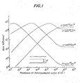
- Fig. 1 shows the relation between the gain in ordinate and the thickness of the semiconductor in abscissa.
- the term of Debye's screening length L D is defined by the following equation. wherein;
- the present invention is to remove the carrier diffusion-phenomenon by using the following 3 kinds of methods.
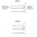
- Fig. 2 shows an embodiment using a thin semiconductor film.
- the reference numeral 1 designates a space in which the electromagnetic field inter-acting with the carrier wave exists
- 2 is an insulating film for protecting the semiconductor surface
- 3 is the thin semiconductor film for producing the carrier wave
- 4 is a semi-insulating substrate for supporting the thin semiconductor film
- d shows the thickness of the thin semiconductor film.
- the thickness d of the thin semiconductor film is preferred to be in an order of the Debye's screening length L D as has been explained with respect to Fig. 1. Furthermore, the thin semiconductor film used in this purpose is preferred to have a high carrier mobility in order to raise the efficiency of the amplification. Under. this object, it is preferred to use the compound semiconductor typically represented by GaAs and InP and mixed crystals thereof. However, Si may be used in view of its highly established processing technique.
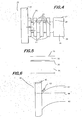
- Fig. 3 shows an embodiment in which the potential barrier against the carrier wave is used.
- the discontinuity of the band at the hetero junction of the semiconductor is used as the barrier for the confinement.
- the reference numeral 11 designates a space in which the electromagnetic field inter-acting with the carrier wave exists
- 12 is an insulating film for protecting the semiconductor surface
- 13 is the semiconductor layer having hetero junction for producing the carrier wave
- 14 is a semi-insulating semiconductor substrate for supporting the semiconductor layer
- d 0 is the thickness of the semiconductor layer having the hetero junction.
- the carriers are confined in the respective low potential semiconductor layers ( 23 )by the barriers accompanying with the hetero junctions.
- the thickness d 1 of the low potential semiconductor layers is preferred to be less than the Debye's screening length. It is better to arrange in a multi-layer construction by stucking number of layers as shown in Fig. 4, by making the thickness of each layer sufficiently thin so as to increase the gain of the device. In this case, the sum of thickness d 1 of the stucked layers may better to exceed the Debye's screening length and the thickness d 2 is better to be thin in a range that the carriers can not move by the tunnel effect. In this embodiment, it is more convenient to additionally use the so called selective doping structure for the portion 24 to increase the mobility of the carriers to further improve the.
- the semiconductors to be used are better to have high carrier mobility for improving the efficiency of the amplification. From this view point, it is preferred to use compound semiconductors typically represented by GaAs and InP and the combination of the mixed crystals such as for instance AlGaAs/GaAs, InAs/GaSb, InP/GaInAs and the like. It is also possible to use combination of Si and Ga.
- Fig. 5 is an embodiment using confinement action of the electric field.
- reference numera 31 is a space in which the electromagnetic field inter-acting with the carrier wave exists
- 32 is an insulating film for protecting the semiconductor surface and for forming the channel layer
- 33 is a channel layer for accumulating (inverting) carriers at the surface of the semiconductor
- 34 is the semiconductor layer.
- Fig. 6 shows potential distribution along the depth of the structure shown in Fig. 5.
- reference numeral41 designates a space in which the electromagnetic wave inter-acting with the carrier wave exists
- 42 is an insulating film for protecting the semiconductor surface and for forming channel layer
- 43 is the channel layer for accumulating (inverting) carriers at the surface of the semiconductor
- 4 4 is the semiconductor layer
- 4 5 shows positive ion caused by doping in the insulating film for forming the accumulating layer at the surface of the semiconductor (in this regard, it is also possible to use gate electrodes for forming the accumulating layer)
- 46 shows Fermi level.
- the electrons in the accumulating layer formed in the surface of the semiconductor are confined by the electric field in the semiconductor layer 44 produced from the positive ions 45 shown in Fig. 6, by the insulating film 42 and by the potential barrier in the semiconductor layer44, namely the electrons are confined in a very narrow region and the diffusion into the bulk of the semiconductor is suppressed.
- the semiconductors used in this structure are preferred to have high carrier mobility in view of improving the efficiency of the amplification and to have less surface level.
- the structure may be combined with hetero structure.
- the present invention is to overcome the loss due to attenuation of the amplitude of the carrier wave inter-acting with the electromagnetic wave by the diffusion of the carrier into semiconductor body by introducing a structure for the confinement of the carrier wave.
- the invention uses as the confinement structure the followng 3 kinds:
Landscapes
- Microwave Amplifiers (AREA)
- Amplifiers (AREA)
- Junction Field-Effect Transistors (AREA)
Applications Claiming Priority (2)
| Application Number | Priority Date | Filing Date | Title |
|---|---|---|---|
| JP62078/85 | 1985-03-28 | ||
| JP60062078A JPH0624263B2 (ja) | 1985-03-28 | 1985-03-28 | 固体電磁波増幅器 |
Publications (3)
| Publication Number | Publication Date |
|---|---|
| EP0196975A2 true EP0196975A2 (de) | 1986-10-08 |
| EP0196975A3 EP0196975A3 (en) | 1988-03-02 |
| EP0196975B1 EP0196975B1 (de) | 1993-05-26 |
Family
ID=13189672
Family Applications (1)
| Application Number | Title | Priority Date | Filing Date |
|---|---|---|---|
| EP86400695A Expired - Lifetime EP0196975B1 (de) | 1985-03-28 | 1986-03-28 | Festkörperverstärker für elektromagnetische Wellen |
Country Status (3)
| Country | Link |
|---|---|
| US (1) | US4847565A (de) |
| EP (1) | EP0196975B1 (de) |
| JP (1) | JPH0624263B2 (de) |
Families Citing this family (4)
| Publication number | Priority date | Publication date | Assignee | Title |
|---|---|---|---|---|
| RU2439751C1 (ru) * | 2010-07-28 | 2012-01-10 | Государственное образовательное учреждение высшего профессионального образования Новгородский государственный университет имени Ярослава Мудрого | Усилитель свч магнитоэлектрический |
| US20130334501A1 (en) * | 2011-09-15 | 2013-12-19 | The Regents Of The University Of California | Field-Effect P-N Junction |
| US9024367B2 (en) | 2012-02-24 | 2015-05-05 | The Regents Of The University Of California | Field-effect P-N junction |
| US10062538B2 (en) * | 2014-10-07 | 2018-08-28 | Nanyang Technological University | Electron device and method for manufacturing an electron device |
Family Cites Families (7)
| Publication number | Priority date | Publication date | Assignee | Title |
|---|---|---|---|---|
| US3336532A (en) * | 1964-03-23 | 1967-08-15 | Bell Telephone Labor Inc | Traveling-wave solid state plasma amplifier with charge flow constraining means |
| US3401347A (en) * | 1966-04-25 | 1968-09-10 | Nippon Telegraph & Telephone | Microwave semiconductor amplifier |
| US3436666A (en) * | 1967-06-05 | 1969-04-01 | Texas Instruments Inc | Solid state traveling wave amplifier |
| US3551831A (en) * | 1968-06-21 | 1970-12-29 | Research Corp | Traveling-wave solid-state amplifier utilizing a semiconductor with negative differential mobility |
| US3639851A (en) * | 1969-06-26 | 1972-02-01 | Thomson Csf | Novel semiconductor amplifier |
| US3621462A (en) * | 1969-12-23 | 1971-11-16 | Rca Corp | Amplifiers and oscillators comprised of bulk semiconductor negative resistance loaded slow-wave structure |
| US3833858A (en) * | 1973-06-15 | 1974-09-03 | Univ Utah | High gain solid-state distributed interaction microwave amplifier |
-
1985
- 1985-03-28 JP JP60062078A patent/JPH0624263B2/ja not_active Expired - Lifetime
-
1986
- 1986-03-28 EP EP86400695A patent/EP0196975B1/de not_active Expired - Lifetime
-
1987
- 1987-12-08 US US07/130,004 patent/US4847565A/en not_active Expired - Fee Related
Also Published As
| Publication number | Publication date |
|---|---|
| EP0196975B1 (de) | 1993-05-26 |
| JPS61222311A (ja) | 1986-10-02 |
| US4847565A (en) | 1989-07-11 |
| JPH0624263B2 (ja) | 1994-03-30 |
| EP0196975A3 (en) | 1988-03-02 |
Similar Documents
| Publication | Publication Date | Title |
|---|---|---|
| US5140386A (en) | High electron mobility transistor | |
| US6028328A (en) | HEMT double hetero structure | |
| US5084743A (en) | High current, high voltage breakdown field effect transistor | |
| EP0170023B1 (de) | Halbleitervorrichtung | |
| US5668387A (en) | Relaxed channel high electron mobility transistor | |
| US4550331A (en) | Multilayer modulation doped heterostructure charge coupled device | |
| EP0196975A2 (de) | Festkörperverstärker für elektromagnetische Wellen | |
| US4344047A (en) | Millimeter-wave power limiter | |
| US3611192A (en) | Bulk semiconductor negative resistance loaded slow-wave device amplifiers and oscillators | |
| US4914743A (en) | Yoked orthogonally distributed equal reactance non-coplanar traveling wave amplifier | |
| US3436666A (en) | Solid state traveling wave amplifier | |
| Adams et al. | Carrier transit delays in nanometer-scale GaAs MESFET's | |
| US4654609A (en) | Monolithic planar doped barrier limiter | |
| RU2093924C1 (ru) | Полевой транзистор на гетероструктуре | |
| US3648185A (en) | Semiconductor device for amplifying microwaves | |
| US3754191A (en) | Semiconductor device for amplifying micro-wave | |
| Ohyama et al. | Impact of 20-MeV/spl alpha/-ray irradiation on the V-band performance of AlGaAs pseudomorphic HEMTs | |
| EP0107039B1 (de) | Resonanzsendehalbleiteranordnung und Schaltung mit dieser Anordnung | |
| Dean et al. | Submicrometer self-aligned dual-gate GaAs FET | |
| US3619801A (en) | Solid-state transferred electron effect device | |
| EP0242652A2 (de) | Bauelement mit Elektronenpotentialtopf | |
| Kuang et al. | Low frequency and microwave characterization of submicron‐gate In0. 52Al0. 48As/In0. 53Ga0. 47As/In0. 52Al0. 48As heterojunction metal‐semiconductor field‐effect transistors grown by molecular‐beam epitaxy | |
| Nakajima et al. | On the frequency dependent drain conductance of ion-implanted GaAs MESFETs | |
| Mikhailov | Experimental study of the parametric interaction between space-charge waves in thin-film GaAs-based semiconductor structures | |
| James | Primary feeds with wide beamwidths |
Legal Events
| Date | Code | Title | Description |
|---|---|---|---|
| PUAI | Public reference made under article 153(3) epc to a published international application that has entered the european phase |
Free format text: ORIGINAL CODE: 0009012 |
|
| AK | Designated contracting states |
Kind code of ref document: A2 Designated state(s): FR GB |
|
| PUAL | Search report despatched |
Free format text: ORIGINAL CODE: 0009013 |
|
| AK | Designated contracting states |
Kind code of ref document: A3 Designated state(s): FR GB |
|
| 17P | Request for examination filed |
Effective date: 19880810 |
|
| 17Q | First examination report despatched |
Effective date: 19901221 |
|
| GRAA | (expected) grant |
Free format text: ORIGINAL CODE: 0009210 |
|
| AK | Designated contracting states |
Kind code of ref document: B1 Designated state(s): FR GB |
|
| ET | Fr: translation filed | ||
| PLBE | No opposition filed within time limit |
Free format text: ORIGINAL CODE: 0009261 |
|
| STAA | Information on the status of an ep patent application or granted ep patent |
Free format text: STATUS: NO OPPOSITION FILED WITHIN TIME LIMIT |
|
| 26N | No opposition filed | ||
| PGFP | Annual fee paid to national office [announced via postgrant information from national office to epo] |
Ref country code: FR Payment date: 19990225 Year of fee payment: 14 |
|
| PGFP | Annual fee paid to national office [announced via postgrant information from national office to epo] |
Ref country code: GB Payment date: 19990401 Year of fee payment: 14 |
|
| PG25 | Lapsed in a contracting state [announced via postgrant information from national office to epo] |
Ref country code: GB Free format text: LAPSE BECAUSE OF NON-PAYMENT OF DUE FEES Effective date: 20000328 |
|
| GBPC | Gb: european patent ceased through non-payment of renewal fee |
Effective date: 20000328 |
|
| PG25 | Lapsed in a contracting state [announced via postgrant information from national office to epo] |
Ref country code: FR Free format text: LAPSE BECAUSE OF NON-PAYMENT OF DUE FEES Effective date: 20001130 |
|
| REG | Reference to a national code |
Ref country code: FR Ref legal event code: ST |