EP0196948A1 - Reversible demultiplexing device of a plurality of light signals in integrated optics - Google Patents
Reversible demultiplexing device of a plurality of light signals in integrated optics Download PDFInfo
- Publication number
- EP0196948A1 EP0196948A1 EP86400499A EP86400499A EP0196948A1 EP 0196948 A1 EP0196948 A1 EP 0196948A1 EP 86400499 A EP86400499 A EP 86400499A EP 86400499 A EP86400499 A EP 86400499A EP 0196948 A1 EP0196948 A1 EP 0196948A1
- Authority
- EP
- European Patent Office
- Prior art keywords
- light
- layer
- guide
- light beam
- light signals
- Prior art date
- Legal status (The legal status is an assumption and is not a legal conclusion. Google has not performed a legal analysis and makes no representation as to the accuracy of the status listed.)
- Granted
Links
Images


Classifications
-
- G—PHYSICS
- G02—OPTICS
- G02B—OPTICAL ELEMENTS, SYSTEMS OR APPARATUS
- G02B6/00—Light guides; Structural details of arrangements comprising light guides and other optical elements, e.g. couplings
- G02B6/10—Light guides; Structural details of arrangements comprising light guides and other optical elements, e.g. couplings of the optical waveguide type
- G02B6/12—Light guides; Structural details of arrangements comprising light guides and other optical elements, e.g. couplings of the optical waveguide type of the integrated circuit kind
- G02B6/12007—Light guides; Structural details of arrangements comprising light guides and other optical elements, e.g. couplings of the optical waveguide type of the integrated circuit kind forming wavelength selective elements, e.g. multiplexer, demultiplexer
-
- G—PHYSICS
- G02—OPTICS
- G02B—OPTICAL ELEMENTS, SYSTEMS OR APPARATUS
- G02B6/00—Light guides; Structural details of arrangements comprising light guides and other optical elements, e.g. couplings
- G02B6/10—Light guides; Structural details of arrangements comprising light guides and other optical elements, e.g. couplings of the optical waveguide type
- G02B6/12—Light guides; Structural details of arrangements comprising light guides and other optical elements, e.g. couplings of the optical waveguide type of the integrated circuit kind
- G02B6/12004—Combinations of two or more optical elements
-
- G—PHYSICS
- G02—OPTICS
- G02B—OPTICAL ELEMENTS, SYSTEMS OR APPARATUS
- G02B6/00—Light guides; Structural details of arrangements comprising light guides and other optical elements, e.g. couplings
- G02B6/10—Light guides; Structural details of arrangements comprising light guides and other optical elements, e.g. couplings of the optical waveguide type
- G02B6/12—Light guides; Structural details of arrangements comprising light guides and other optical elements, e.g. couplings of the optical waveguide type of the integrated circuit kind
- G02B6/122—Basic optical elements, e.g. light-guiding paths
- G02B6/124—Geodesic lenses or integrated gratings
-
- G—PHYSICS
- G02—OPTICS
- G02B—OPTICAL ELEMENTS, SYSTEMS OR APPARATUS
- G02B6/00—Light guides; Structural details of arrangements comprising light guides and other optical elements, e.g. couplings
- G02B6/24—Coupling light guides
- G02B6/26—Optical coupling means
- G02B6/28—Optical coupling means having data bus means, i.e. plural waveguides interconnected and providing an inherently bidirectional system by mixing and splitting signals
- G02B6/293—Optical coupling means having data bus means, i.e. plural waveguides interconnected and providing an inherently bidirectional system by mixing and splitting signals with wavelength selective means
- G02B6/29304—Optical coupling means having data bus means, i.e. plural waveguides interconnected and providing an inherently bidirectional system by mixing and splitting signals with wavelength selective means operating by diffraction, e.g. grating
- G02B6/29316—Light guides comprising a diffractive element, e.g. grating in or on the light guide such that diffracted light is confined in the light guide
- G02B6/29325—Light guides comprising a diffractive element, e.g. grating in or on the light guide such that diffracted light is confined in the light guide of the slab or planar or plate like form, i.e. confinement in a single transverse dimension only
-
- G—PHYSICS
- G02—OPTICS
- G02B—OPTICAL ELEMENTS, SYSTEMS OR APPARATUS
- G02B6/00—Light guides; Structural details of arrangements comprising light guides and other optical elements, e.g. couplings
- G02B6/24—Coupling light guides
- G02B6/26—Optical coupling means
- G02B6/28—Optical coupling means having data bus means, i.e. plural waveguides interconnected and providing an inherently bidirectional system by mixing and splitting signals
- G02B6/293—Optical coupling means having data bus means, i.e. plural waveguides interconnected and providing an inherently bidirectional system by mixing and splitting signals with wavelength selective means
- G02B6/29379—Optical coupling means having data bus means, i.e. plural waveguides interconnected and providing an inherently bidirectional system by mixing and splitting signals with wavelength selective means characterised by the function or use of the complete device
- G02B6/2938—Optical coupling means having data bus means, i.e. plural waveguides interconnected and providing an inherently bidirectional system by mixing and splitting signals with wavelength selective means characterised by the function or use of the complete device for multiplexing or demultiplexing, i.e. combining or separating wavelengths, e.g. 1xN, NxM
Abstract
Dispositif réversible de démultiplexage de plusieurs signaux lumineux en optique intégrée. Ce dispositif réversible servant notamment à séparer n signaux lumineux de longueurs d'onde différentes (λ1,... λn) formant un faisceau lumineux (4) transporté par une première fibre optique (2) et à réinjecter respectivement dans n secondes fibres optiques (F1,... Fn) les n signaux lumineux comprend, réalisés dans un guide de lumière (6), une optique d'entrée achromatique (18) servant à rendre parallèle ledit faisceau lumineux, n réseaux (R1,... Rn) disposés en cascade, travaillant en régime de Bragg, chaque réseau servant à diffracter la partie du faisceau lumineux transportant l'un des n signaux lumineux et à transmettre la partie non encore diffractée dudit faisceau lumineux en direction du réseau suivant, et n optiques de sortie (M1,..., Mn) associées aux n réseaux, chaque optique de sortie servant à focaliser ladite partie du faisceau lumineux diffractée par le réseau associé.Reversible device for demultiplexing several light signals in integrated optics. This reversible device serving in particular to separate n light signals of different wavelengths (λ1, ... λn) forming a light beam (4) transported by a first optical fiber (2) and to reinject respectively into n second optical fibers ( F1, ... Fn) the n light signals comprises, produced in a light guide (6), an achromatic input optic (18) used to make said light beam parallel, n networks (R1, ... Rn) arranged in cascade, working in Bragg regime, each grating serving to diffract the part of the light beam carrying one of the n light signals and to transmit the not yet diffracted part of said light beam towards the next grating, and n output optics (M1, ..., Mn) associated with the n networks, each output optic serving to focus said part of the light beam diffracted by the associated network.
Description
La présente invention a pour objet un dispositif servant à multiplexer ou démultiplexer plusieurs signaux lumineux en optique intégrée. Elle trouve une application notamment dans les domaines des traitements de signaux radars en temps réel, des télécommunications par voie optique, des capteurs à fibre optique, etc...The present invention relates to a device for multiplexing or demultiplexing several light signals in integrated optics. It finds an application in particular in the fields of radar signal processing in real time, optical telecommunications, fiber optic sensors, etc.
Le multiplexage de signaux lumineux de longueurs d'onde différentes, en optique intégrée, est un point important dans les télécommunications optiques puisqu'il permet de transporter dans une même fibre optique une grande quantité d'informations à bandes passantes constantes.The multiplexing of light signals of different wavelengths, in integrated optics, is an important point in optical telecommunications since it makes it possible to transport a large quantity of information with constant bandwidths on the same optical fiber.
Un dispositif de démutfiplexage ou un démultiplexeur, en optique intégrée, est un dispositif qui permet de séparer n signaux lumineux de longueurs d'onde différentes transportés par une même première fibre optique et de réinjecter 0respectivement dans n secondes fibres optiques lesdits n signaux tumineux. Inversement un dispositif de muttiplexage ou multiplexeur est un dispositif qui permet de regrouper en un seul faisceau, n signaux lumineux de longueurs d'onde différentes issues respectivement de n fibres optiques.A demutfiplexing device or a demultiplexer, in integrated optics, is a device which makes it possible to separate n light signals of different wavelengths transported by the same first optical fiber and to reinject 0respectively into n second optical fibers said n signals. Conversely, a multiplexing or multiplexer device is a device which makes it possible to group together in a single beam, n light signals of different wavelengths originating respectively from n optical fibers.
Dans de tels dispositifs, deux problèmes importants se posent Le premier problème est d'assurer la fonction multiplexeur, c'est-à-dire qu'en sortie du dispositif la ième seconde fibre optique, i étant un entier allant de 1 à n, ne doit transporter que la longueur d'onde λi à Dλ/2 près. L'élément de multiplexage idéal est donc un filtre créneau, de largeur ± Δλ/2 et de transmission 1 si λi-Δλ/2 λ λi+Δλ/2, qui réfléchirait ou au contraire transmettrait parfaitement les signaux lumineux dont les longueurs d'onde ne sont pas comprises dans cet intervalle et inversement transmettrait ou réfléchirait ceux dont les longueurs d'onde sont comprises dans cet intervalle. Une succession de tels filtres constituerait un dispositif de multiplexage idéal.In such devices, two important problems arise. The first problem is to ensure the multiplexer function, that is to say that at the output of the device the ith second optical fiber, i being an integer ranging from 1 to n, should only carry the wavelength λ i to within Dλ / 2. The ideal multiplexing element is therefore a niche filter, of width ± Δλ / 2 and of transmission 1 if λ i -Δλ / 2 λ λ i + Δλ / 2, which would reflect or on the contrary perfectly transmit the light signals whose lengths wavelengths are not included in this interval and conversely would transmit or reflect those whose wavelengths are included in this interval. A succession of such filters would constitute an ideal multiplexing device.
Le deuxième problème important est le couplage du dispositif de multiplexage avec les fibres optiques généralement monomodes, transportant les informations lumineuses. En effet, les pertes lumineuses à l'entrée et à la sortie du dispositif de multiplexage doivent être les plus faibles possibles.The second important problem is the coupling of the multiplexing device with the generally single-mode optical fibers, transporting the light information. In fact, the light losses at the input and at the output of the multiplexing device must be as low as possible.
Dans les disposififs de multiplexage actuellement connus en optique intégrée, la fonction multiplexeur, c'est-à-dire la dispersion chromatique des différents signaux lumineux est assurée par un réseau, comme en optique classique. Un tel dispositif de multiplexage est notamment décrit dans un article de Applied Optics, vol. 21, n°12, du 15 juin 1982, pages 2195 à 2198 de T. SUHARA et al. intitulé "Integrated-Optc wavelength multi-and demultplexers using a chirped grating and an ion-exchanged waveguide".In the multiplexing devices currently known in integrated optics, the multiplexer function, that is to say the chromatic dispersion of the different light signals is provided by a network, as in conventional optics. Such a multiplexing device is described in particular in an article by Applied Optics, vol. 21, n ° 12, of June 15, 1982, pages 2195 to 2198 of T. SUHARA et al. titled "Integrated-Optc wavelength multi-and demultplexers using a chirped grating and an ion-exchanged waveguide".
Malheureusement, ces dispositifs de multiplexage ne résolvent pas le problème le plus important concernant le couplage du multiplexeur et des fibres optiques monomodes utilisées pour le transport des informations lumineuses ainsi que celui de la collimation du faisceau lumineux qui attaque l'élément dispersif ou réseau du dispositif de multiplexage.Unfortunately, these multiplexing devices do not solve the most important problem concerning the coupling of the multiplexer and the single-mode optical fibers used for the transport of light information as well as that of the collimation of the light beam which attacks the dispersive or network element of the device. multiplexing.
La présente invention a justement pour objet un dispositif de démultiplexage réversible de plusieurs signaux lumineux en optique intégrée permettant de remédier aux différents inconvénients donnés ci-dessus. En particulier, il permet un bon couplage avec les fibres optiques utilisées pour le transport des informations et donc de faibles pertes de lumière.The subject of the present invention is precisely a device for reversible demultiplexing of several light signals in integrated optics making it possible to remedy the various drawbacks given above. In particular, it allows good coupling with the optical fibers used for transporting information and therefore low light losses.
De plus, il permet, de façon plus aisée que les dispositifs de l'art antérieur, le multiplexage de plusieurs signaux lumineux de longueurs d'onde différentes, par exemple jusqu'à huit signaux, tout en conservant des pertes totales lumineuses acceptabtes. Par ailleurs, le dispositif de multiplexage ou de multiplexage de l'invention peut être réalisé selon une technologie parfaitement reproductible.In addition, it allows, more easily than the devices of the prior art, the multiplexing of several light signals of different wavelengths, for example up to eight signals, while retaining acceptable total light losses. Furthermore, the multiplexing or multiplexing device of the invention can be produced according to a perfectly reproducible technology.
La présente invention a justement pour objet un dispositif de démultiplexage intégré servant à séparer n signaux lumineux de longueurs d'onde différentes, constituant un faisceau lumineux incident transporté par une première fibre optique, et à réinjecter respectivement dans n secondes fibres optiques les n signaux lumineux, ce dispositif, formé de composants optiques réalisés dans au moins un guide de lumière, étant caractérisé en ce qu'il comprend, réalisés dans le guide :
- -une optique d'entrée achromatique servant à rendre parallèle le faisceau lumineux incident sortant de la première fibre optique,
- -au moins n réseaux disposés en cascade, travaillant en régime de Bragg, chaque réseau servant à diffracter une première partie du faisceau lumineux et à transmettre une seconde partie dudit faisceau lumineux, l'une des deux parties ne transportant que l'un des n signaux lumineux, l'autre partie, transportant les autres signaux lumineux, étant envoyée en direction du réseau suivant, et
- -n optiques de sortie associées aux n réseaux, chaque . optique de sortie servant à focaliser la partie du faisceau lumineux ne transportant que l'un des n signaux lumineux, et en ce qu'il est réversible.
- an achromatic input optic used to make the incident light beam leaving the first optical fiber parallel,
- at least n networks arranged in cascade, working in Bragg regime, each network serving to diffract a first part of the light beam and to transmit a second part of said light beam, one of the two parts carrying only one of the n light signals, the other party, carrying the other light signals, being sent towards the next network, and
- -n output optics associated with the n networks, each. output optics used to focus the part of the light beam carrying only one of the n light signals, and in that it is reversible.
Le dispositif selon t'invention est réversible, c'est-à-dire qu'il permet soit le démultiplexage, soit le multiplexage de signaux lumineux. Dans le sens multiplexage, le dispositif sert à injecter dans la première fibre un faisceau lumineux sortant, contenant n signaux lumineux issus respectivement de n secondes fibres optiques- Dans ce cas, l'optique d'entrée joue le rôle d'optique de sortie ; les réseaux servent à combiner deux faisceaux lumineux et les n optiques de sorties jouent le rôle de n optiques d'entrée.The device according to the invention is reversible, that is to say it allows either demultiplexing or multiplexing of light signals. In the multiplexing direction, the device is used to inject an outgoing light beam into the first fiber, containing n light signals originating respectively from n second optical fibers. In this case, the input optics plays the role of output optics; the arrays are used to combine two light beams and the n output optics play the role of n input optics.
Dans la suite du texte le dispositif selon l'invention sera décrit dans le sens démultiplexage.In the following text, the device according to the invention will be described in the demultiplexing direction.
L'optique d'entrée achromatique, qui est avantageusement un miroir parabolique, assure la collimation du faisceau lumineux devant être traité dans le dispositif de multiplexage. Il permet ainsi aux réseaux de travailler en régime de Bragg et donc d'assurer une bonne sélection en longueur d'onde.The achromatic input optic, which is advantageously a parabolic mirror, collimates the light beam to be processed in the multiplexing device. It thus allows networks to work in the Bragg regime and therefore to ensure good wavelength selection.
Selon un mode préféré de réalisation du dispositif de l'invention, la partie ne transportant que l'un des n signaux lumineux est la partie du faisceau lumineux diffractée parle réseau correspondantAccording to a preferred embodiment of the device of the invention, the part carrying only one of the n light signals is the part of the light beam diffracted by the corresponding network
De façon avantageuse, le dispositif selon l'invention comprend un microguide d'entrée, intercalé entre la première fibre optique et l'optique d'entrée, ayant une structure voisine de celle de la première fibre optique etIou des microguides de sortie, intercalés respectivement entre les n optiques de sortie et les n secondes fibres optiques, ayant respectivement une structure voisine de celles des secondes fibres optiques.Advantageously, the device according to the invention comprises an input microguide, interposed between the first optical fiber and the input optic, having a structure close to that of the first optical fiber and or output microguides, interposed respectively between the n output optics and the n second optical fibers, respectively having a structure close to that of the second optical fibers.
L'utilisation d'un microguide d'entrée et de n microguides de sortie, ayant une structure très voisine de celle respectivement des fibres optiques d'entrée et de sortie, permet d'assurer un bon couplage entre ces fibres et le dispositif de multiplexage, limitant ainsi les pertes lumineuses à l'entrée et à la sortie du dispositif. De préférence, les microguides de sortie du dispositif de multiplexage sont courbes.The use of an input microguide and of n output microguides, having a structure very close to that of the input and output optical fibers respectively, makes it possible to ensure good coupling between these fibers and the multiplexing device, thus limiting the light losses at the entry and exit of the device. Preferably, the output microguides of the multiplexing device are curved.
Selon un autre mode préféré de réalisation du dispositif de l'invention, les optiques de sortie de ce dispositif sont des miroirs paraboliques achromatiques; ces miroirs permettent une bonne focalisation des faisceaux lumineux entrant respectivement dans les différentes secondes fibres optiques.According to another preferred embodiment of the device of the invention, the output optics of this device are achromatic parabolic mirrors; these mirrors allow good focusing of the light beams entering the different second optical fibers respectively.
Selon un autre mode préféré de réalisation du dispositif de l'invention, les composants optiques sont formés dans deux guides de lumière superposés, un guide inférieur de forte variation d'indice et un guide supérieur de plus faible variation d'indice dans lequel se propage le faisceau lumineux incident. Dans une telle structure, le dispositif de multiplexage comprend n premiers réseaux servant chacun à diffracter une première partie du faisceau lumineux et à transmettre une seconde partie dudit faisceau lumineux, l'une des deux parties ne transportant que l'un des n signaux lumineux, l'autre partie, transportant les autres signaux lumineux, étant envoyée en direction du premier réseau suivant, la partie ne transportant que l'un des n signaux lumineux étant alors transférée du guide supérieur au guide inférieur, ainsi que n seconds réseaux associés auxdits premiers servant chacun à retransférer la partie du faisceau lumineux ne transportant que l'un des n signaux lumineux du guide inférieur au guide supérieur.According to another preferred embodiment of the device of the invention, the optical components are formed in two superimposed light guides, a lower guide with large index variation and an upper guide with small index variation in which propagates the incident light beam. In such a structure, the multiplexing device comprises n first gratings each serving to diffract a first part of the light beam and to transmit a second part of said light beam, one of the two parts carrying only one of the n light signals, the other part, transporting the other light signals, being sent in the direction of the first following network, the part transporting only one of the n light signals then being transferred from the upper guide to the lower guide, as well as n second networks associated with said first each serving to retransfer the part of the light beam carrying only one of the n light signals from the lower guide to the upper guide.
L'utilisation de deux guides de lumière superposés permet, si nécessaire, de traiter les signaux lumineux lors de leur propagation dans le guide de lumière à forte variation d'indice.The use of two superimposed light guides makes it possible, if necessary, to process the light signals during their propagation in the light guide with large index variation.
De façon avantageuse, les éléments optiques du dispositif de multiplexage sont formés par gravure d'au moins une partie du guide de lumière.Advantageously, the optical elements of the multiplexing device are formed by etching at least part of the light guide.
Selon un autre mode préféré de réalisation du dispositif de l'invention, le guide de lumière comprend, réalisées dans l'ordre sur un substrat en silicium, une première couche d'oxyde de silicium non dopé, une seconde couche d'oxyde de silicium dopé et une troisième couche d'oxyde de silicium éventuellement dopé avec un élément diminuant l'indice de réfraction de cette troisième couche, le dopage du matériau de la seconde couche étant tel que son indice de réfraction est supérieur à celui des première et troisième couches.According to another preferred embodiment of the device of the invention, the light guide comprises, produced in order on a silicon substrate, a first layer of undoped silicon oxide, a second layer of silicon oxide doped and a third layer of silicon oxide optionally doped with an element reducing the refractive index of this third layer, the doping of the material of the second layer being such that its refractive index is greater than that of the first and third layers .
Selon un autre mode préféré de réalisation du dispositif de l'invention, les deux guides de lumière comprennent, réalisées dans l'ordre sur un substrat semiconducteur notamment en silicium, une première couche par exemple d'oxyde de silicium non dopé, une seconde couche notamment de nitrure de silicium, une troisième couche par exemple d'oxyde de silicium dopé et une quatrième couche notamment d'oxyde de silicium éventuellement dopé avec un élément diminuant l'indice de réfraction de cette quatrième couche, la troisième couche étant telle que son indice de réfraction est supérieur à celui des première et quatrième couches et inférieur à celui de la seconde couche, les première, seconde et troisième couches formant le guide de lumière inférieur et les première, troisième et quatrième couches formant le guide de lumière supérieur.According to another preferred embodiment of the device of the invention, the two light guides comprise, produced in order on a semiconductor substrate, in particular made of silicon, a first layer, for example of undoped silicon oxide, a second layer in particular of silicon nitride, a third layer for example of doped silicon oxide and a fourth layer in particular of silicon oxide optionally doped with an element reducing the refractive index of this fourth layer, the third layer being such that its refractive index is higher than that of the first and fourth layers and lower than that of the second layer, the first, second and third layers forming the lower light guide and the first, third and fourth layers forming the upper light guide.
D'autres caractéristiques et avantages de l'invention ressortiront mieux de la description qui va suivre, donnée à titre illustratif et non limitatif, en référence aux figures annexées, dans lesquelles :
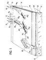
- -la figure 1 représente schématiquement, en perspective, un dispositif de multiplexage conformément à l'invention réalisé dans un seul guide de lumière,
- - la figure 2 représente schématiquement, en vue de dessus, le dispositif de multiplexage de la figure 1,
- la figure 3 représente schématiquement l'élément d'entrée du dispositif de la figure 1 assurant la collimation du faisceau lumineux à traiter,
- -les figures 4a et 4b représentent respectivement, en coupe longitudinale, deux structures possibles pour le réseau du dispositif de multiplexage conformément à l'invention, et
- -la figure 5 représente schématiquement, en vue de dessus, un dispositif de multiplexage conformément à l'invention réalisé dans deux guides de lumière superposés.
- FIG. 1 schematically represents, in perspective, a multiplexing device according to the invention produced in a single light guide,
- FIG. 2 schematically represents, in top view, the multiplexing device of FIG. 1,
- FIG. 3 schematically represents the input element of the device of FIG. 1 ensuring the collimation of the light beam to be treated,
- FIGS. 4a and 4b respectively represent, in longitudinal section, two possible structures for the network of the multiplexing device according to the invention, and
- FIG. 5 schematically represents, in top view, a multiplexing device according to the invention produced in two superimposed light guides.
Sur les figures 1 et 2, on a représenté - schématiquement un dispositif de multiplexage intégré selon l'invention servant à séparer n signaux lumineux, respectivement de longueurs d'onde X,, λ2,..., Xn, transportés par une première fibre optique 2, notamment en silice, et à réinjecter respectivement dans n secondes fibres optiques F,, F.,... Fn, les n signaux lumineux. En particulier, la fibre optique F, ne reçoit que le signal lumineux de longueur d'onde λ1,... et la fibre optique Fn ne reçoit que le signal lumineux de longueur d'onde Xn . Les longueurs d'onde X,, λ2,..., Xn peuvent être comprises entre 0,7 µm et 1,8 µm. Les n signaux lumineux transportés par la première fibre optique 2 forment un unique faisceau lumineux incident 4.In Figures 1 and 2, there is shown - schematically an integrated multiplexing device according to the invention used to separate n light signals, respectively of wavelengths X ,, λ 2 , ..., X n , transported by a first optical fiber 2, in particular made of silica, and to be injected respectively into n second optical fibers F ,, F., ... Fn, the n light signals. In particular, the optical fiber F, receives only the light signal of wavelength λ 1 , ... and the optical fiber F n receives only the light signal of wavelength X n . The wavelengths X ,, λ 2 , ..., X n can be between 0.7 µm and 1.8 µm. The n light signals transported by the first optical fiber 2 form a single
Ce dispositif de multiplexage comprend, comme représenté sur la figure 1, un guide de lumière 6 réalisé sur un substrat semiconducteur monocristatiin 8 par exemple en silicium ou formé de matériau III-V tel que le GaAs. Le substrat est obtenu par clivage d'un bloc semiconducteur afin de présenter des faces E et S rigoureusement parallèles.This multiplexing device comprises, as shown in FIG. 1, a light guide 6 produced on a
Le guide de lumière 6 est constitué de trois couches superposées respectivement 10, 12 et 14. La couche 12, intercalée entre les couches 10 et la couche 14, constitue la couche guidante du guide. Elle présente un indice de réfraction supérieur à celui des couches 10 et 14. Par exemple, la couche inférieure 10 surmontant le substrat 8 est réalisée en oxyde de silicium pur, la couche 12 en oxyde de silicium dopé notamment au phosphore, au germanium ou au titane, et la couche supérieure 14 en oxyde de silicium pur ou dopé avec un élément tel que le bore ou le fluor, diminuant l'indice de réfraction de ladite couche. Les couches d'oxyde pur 10 et 14 présentent, pour une même longueur d'environ 0,8 um, un indice de réfraction par exemple de 1,45 pour de l'oxyde pur et la couche d'oxyde dopé 12 un indice de 1,46. Ce guide de lumière à faible variation d'indice présente des caractéristiques voisines de celles des fibres optiques monomodes en silice généralement utilisées en optique intégrée ; sa faible variation d'indice permet de rester monomode même pour une couche guidante 12 de 10 um.The light guide 6 consists of three superimposed
Dans ce guide de lumière 6, sont intégrés les différents composants optiques du dispositif de multiplexage.In this light guide 6, the various optical components of the multiplexing device are integrated.
Le dispositif de multiplexage comprend à son entrée E un microguide 16, permettant d'assurer un bon couplage entre la première fibre optique 2 transportant les signaux lumineux de longueurs d'onde différentes et le dispositif de multiplexage. Ce microguide 16 d'entrée présente une structure très voisine de celle constituant la fibre optique 2 qui est notamment une fibre monomode réalisée en silice ou oxyde de silicium. Ce microguide 16, comme représenté sur la figure 2, est de préférence un microguide rectiligne.The multiplexing device comprises at its input E a
Une optique achromatique 18 telle qu'un miroir achromatique de forme parabolique permet de collimater le faisceau lumineux 4, issu du microguide d'entrée 16 et contenant les signaux lumineux de longueurs d'onde différentes. Autrement dit, cette optique 18 permet de transformer, comme représenté sur la figure 3, la lumière sortant du microguide 16 assimilée à un point lumineux P en un faisceau de lumière parallèle 20 ; pour ce faire, le point lumineux P doit être situé au foyer de l'optique 18.
Le faisceau de lumière parallèle 20 issu du miroir parabolique 18, comme représenfé sur la figure 2, attaque n réseaux R1, R2,..., R n disposés en cascade et travaillant en régime de Bragg. Ces réseaux sont des structures périodiques ; ils comportent, sous forme de bandes parallèles régulièrement espacées, une alternance de creux et de bosses (figure 4a).The
Le premier réseau R1 permet par exemple de diffracter la partie du faisceau lumineux 22 transportant le signal lumineux ayant la longueur d'onde λ1, et de transmettre le reste 24 du faisceau lumineux, contenant les autres signaux lumineux. La partie 24 du faisceau incident 20 transmise par le premier réseau R, est reçue par le second réseau R2- Ce dernier diffracte à son tour la partie 26 du faisceau lumineux 24 contenant le signal optique de longueur d'onde λ2 et transmet le reste 28 du signal lumineux 24, sur le troisième réseau R3. Ainsi de suite, les n signaux lumineux de longueurs d'onde différentes respectivement λ1, λ2,...,λn sont séparés les uns des autres et envoyés vers les fibres optiques F1, F2,..., Fn correspondantes.The first grating R 1 makes it possible, for example, to diffract the part of the
L'angte de Bragg ou d'attaque αi du réseau Ri, i étant un entier allant de 1 à n, repéré par rapport à la normale audit réseau, est choisi en fonction des possibilités de réalisation technologique de la structure des différents réseaux. Cet angle αi dépend de la longueur d'onde λi à diffracter ainsi que du pas du réseau pi correspondant En particulier, le ième réseau Ri peut être déterminé de façon qu'il réfléchisse la longueur d'onde λi et transmette les autres. Pour cela, il faut que λi=2pisinαi-Cette condition peut être réalisée en choisissant le pas pi du réseau Ri et en faisant varier αi pour effectuer la sélection en longueur d'onde ou bien garder αi constant et faire varier le pas pi du réseau. Pour des raisons pratiques de réalisation des différents réseaux R1, R2,..., Rn, il est préférable de fixer le pas pi et de faire varier αi.The Bragg or attack angle α i of the network R i , i being an integer ranging from 1 to n, identified with respect to the normal to said network, is chosen according to the possibilities of technological realization of the structure of the different networks . This angle α i depends on the wavelength λ i to be diffracted as well as on the pitch of the corresponding network p i In particular, the ith network R i can be determined so that it reflects the wavelength λ i and transmits others. For that, it is necessary that λ i = 2pisinα i- This condition can be realized by choosing the pitch p i of the network R i and by varying α i to make the selection in wavelength or else keep α i constant and make vary the network pitch pi. For practical reasons of realization of the various networks R 1 , R 2 , ..., R n , it is preferable to fix the pitch p i and to vary α i .
Après les réseaux R,, R2,..., Rn, les faisceaux lumineux diffractés, tels que 22 et 26, ne sont plus rigoureusement des faisceaux parallèles. Or, comme tous ces faisceaux doivent sortir perpendiculairement à une face clivée du substrat en silicium 8, c'est-à-dire parallèlement ou perpendiculairement à la face d'entrée E du guide de lumière, par exempte la face parallèle S, n éléments optiques M1, M2,..., Mn sont prévus pour focaliser les faisceaux lumineux diffractés par les différents réseaux. Chaque miroir Mi est associé à un réseau Ri et il permet de focaliser la partie du faisceau lumineux diffractée par ce réseau Ri.After the networks R ,, R 2 , ..., R n , the diffracted light beams, such as 22 and 26, are no longer strictly parallel beams. However, as all these beams must exit perpendicular to a cleaved face of the
De façon à améliorer le couplage en sortie du dispositif de multiplexage avec les différentes fibres optiques F,, F2,... Fn, n microguides de lumière respectivement G1, G2,..., Gn sont intercalés respectivement entre les miroirs M1, M2,..., Mn et les fibres optiques F1, F2,..., Fn. Chaque microguide Gi présente une structure très voisine de la fibre optique F icorrespondante recevant le signal lumineux de longueur d'onde λi-. Comme pour le microguide d'entrée 16 (figure 3) les foyers des éléments optiques M,, M2,..., Mn sont situés juste à l'entrée des microguides G1, G2,..., Gncorrespondants.In order to improve the coupling at the output of the multiplexing device with the different optical fibers F ,, F 2 , ... F n , n light microguides respectively G 1 , G 2 , ..., G n are interposed respectively between the mirrors M 1 , M 2 , ..., M n and the optical fibers F 1 , F 2 , ..., F n . Each microguide G i has a structure very close to the corresponding optical fiber F i receiving the light signal of wavelength λ i -. As for the input microguide 16 (FIG. 3), the focal points of the optical elements M ,, M 2 , ..., M n are located just at the entrance of the microguides G 1 , G 2 , ..., G n correspondents.
De préférence, ces microguides présentent une forme courbe, ce qui contribue à faire sortir les différents signaux lumineux diffractés par les réseaux R,, R2,..., Rn, transportant respectivement le signal lumineux λ1, λ2,..., λn, perpendiculairement à la face clivée S du substrat monocristallin 8 de silicium.Preferably, these microguides have a curved shape, which contributes to bringing out the different light signals diffracted by the networks R ,, R 2 , ..., R n , respectively transporting the light signal λ 1 , λ 2 , .. ., λn, perpendicular to the cleaved face S of the
On va maintenant décrire un procédé de fabrication du dispositif de multiplexage décrit précédemment, dans le cas d'un substrat en silicium monocristallin et d'un guide de lumière en oxyde de silicium.We will now describe a method of manufacturing the multiplexing device described above, in the case of a monocrystalline silicon substrate and a light guide of silicon oxide.
La première étape consiste à faire croître par oxydation thermique du substrat la couche inférieure 10 d'oxyde de silicium allant de 1 à 5 µm d'épaisseur. Cette croissance peut être obtenue à basse température entre 800 et 850°C et sous une pression d'environ 106 Pa ou à plus haute température entre 1000°C et 1150°C sous pression atmosphérique.The first step consists in growing by thermal oxidation of the substrate the
On dépose ensuite par un procédé de dépôt chimique en phase vapeur, assisté ou non par plasma, la couche 12 d'oxyde de silicium 3 dopé au phosphore, au germanium ou au titane. Cette couche d'oxyde de silicium dopé présente une épaisseur allant de 4 à 10 µm. En jouant sur la quantité de dopant introduit, par exemple de 1021 à 1022 atomes/cm3 pour le phosphore, on peut adapter la différence d'indice entre la couche dopée 12 et les couches inférieure 10 et supérieure 14 ; une différence d'indice de 10-3 peut être suffisante.Then deposited by a chemical vapor deposition process, assisted or not by plasma, the
La troisième couche d'oxyde de silicium peut être déposée par un procédé de dépôt chimique en phase vapeur assisté ou non par ptasma Cette couche 14 peut être en oxyde pur ou dopé avec un élément qui diminue l'indice de réfraction de cette couche, tel que le bore ou le fluor Cette couche supérieure représente une épaisseur allant de 1 à 6 µm.The third layer of silicon oxide can be deposited by a chemical vapor deposition process assisted or not by plasma. This
Les étapes suivantes consistent à graver le guide de lumière ainsi réalisé, travers un masque approprié, selon les procédés classiques de photolithographie, de façon à former les différents composants optiques.The following steps consist in etching the light guide thus produced, through an appropriate mask, according to conventional photolithography methods, so as to form the various optical components.
Afin d'obtenir des éléments optiques de forme parfaitement définie, on utilisera une gravure anisotrope comme par exemple une gravure ionique réactive utilisant comme agent d'attaque du tétrafiuorure de carbone ou du trifiuo- rométhane.In order to obtain optical elements of perfectly defined shape, an anisotropic etching will be used such as, for example, reactive ion etching using as an attack agent carbon tetrafluoride or trifiuouroethane.
Pour former le microguide d'entrée 16 et les microguides de sortie G1, G2,..., Gn, on peut uniquement éliminer les parties de la couche supérieure d'oxyde de silicium 14 non en regard de la fibre optique 2 d'amenée des signaux et des fibres optiques F,, F2,..., Fn de sortie desdits signaux, comme représenté sur la figure 1.To form the input microguide 16 and the output microguides G 1 , G 2 , ..., G n , it is only possible to remove the parts of the upper layer of
Pour former les miroirs paraboliques d'entrée 18 et de sortie M1, M2,..., Mn, on peut éliminer, aux emplacements prévus pour ces miroirs, simultanément les trois couches d'oxyde 10, 12 et 14.To form the
Pour ce qui est des réseaux R,, R2,..., Rn, on peut éliminer, comme représenté sur la figure 4a, aux emplacements prévus pour lesdits résaux, la couche supérieure 14 du guide de lumière et partiellement la couche guidante 12. La profondeur des sillons gravés h est déterminée par la bande passante Δλ désirée qui dépend de la force du réseau. Plus la profondeur h est élevée, plus la sélection en longueur d'onde est fine (Δλ faible).As for the networks R ,, R 2 , ..., Rn , it is possible to eliminate, as shown in FIG. 4a, at the locations provided for said networks, the
Dans une variante du procédé de fabrication du dispositif de l'invention, on ne réalise que le dépôt de la couche inférieure 10 et de la couche guidante 12 du guide de lumière, selon les mêmes techniques de dépôt Puis, à l'aide d'un masque approprié, défini selon les procédés classiques de photolithographie, on grave partiellement la couche guidante 12, comme représenté sur la figure 4b, afin de former les différents réseaux. Cette gravure est notamment une gravure anisotrope comme une gravure ionique réactive.In a variant of the method of manufacturing the device of the invention, only the deposition of the
Après cette gravure, on dépose sur l'ensemble de la structure une couche d'oxyde de silicium pur, dont l'épaisseur correspond à celle de la couche supérieure 14 du guide de lumière. Ce dépôt peut être réalisé par un procédé de dépôt chimique en phase vapeur assisté par plasma.After this etching, a layer of pure silicon oxide is deposited over the entire structure, the thickness of which corresponds to that of the
Les autres éléments optiques (miroirs, microguides) sont réalisés comme précédemment par gravure d'une ou plusieurs couches du guide de lumière.The other optical elements (mirrors, microguides) are produced as before by etching one or more layers of the light guide.
Sur la figure 5, on a représenté en perspective un autre mode de réalisation du dispositif de multiplexage conformément à l'invention. Les éléments optiques de ce dispositif jouant les mêmes rôles que ceux décrits précédemment, en référence aux figures 1 et 2, porteront les mêmes références suivies d'un indice a ou d'un symbole '.In Figure 5, there is shown in perspective another embodiment of the multiplexing device according to the invention. The optical elements of this device playing the same roles as those described above, with reference to Figures 1 and 2, will bear the same references followed by an index a or a symbol '.
Ce dispositif de multiplexage permet de séparer n signaux lumineux de longueur d'onde λ1, λ2,..., λn transportés par la fibre optique 2 et de les réinjecter respectivement dans les n secondes fibres optiques F1, F2,..., Fn. Ce dispositif comprend deux guides de lumière superposés 6a, un guide inférieur de forte variation d'indice et un guide supérieur de plus faible variation d'indice.This multiplexing device makes it possible to separate n light signals of wavelength λ 1 , λ 2 , ..., λ n transported by the optical fiber 2 and to reinject them respectively into the n second optical fibers F 1 , F 2 , ..., F n . This device comprises two superimposed light guides 6a, a lower guide with large index variation and an upper guide with small index variation.
Ces deux guides de lumière superposés 6a sont réalisés sur un substrat semiconducteur monocristallin 8a notamment en silicium et sont constitués par un empilement de quatre couches portant respectivement les références 10a, 11, 12a, 14a. Les couches médianes 11 et 12a correspondent respectivement aux couches guidantes du guide inférieur et du guide supérieur. La couche 11 présente un indice de réfraction supérieur à celui des couches 10a et 12a entrant dans la constitution du guide inférieur et la couche 12a présente un indice de réfraction supérieur à celui de la couche 10a et de la couche 14a entrant dans la constitution du guide de lumière supérieur.These two superimposed light guides 6a are produced on a
Pour un substrat 8a en silicium, la couche 10a peut être réalisée en oxyde de silicium non dopé, obtenu par exemple par oxydation thermique du substrat à 800-850°C sous 106 Pa ou à plus haute température, entre 1000°C et 1150°C sous pression atmosphérique ; elle présente par exemple un indice de réfraction de l'ordre de 1,58 pour une longueur d'onde de 0,8 µm et une épaisseur de 1 à 5 u.m. La couche 11 est avantageusement réalisée en nitrure de silicium, matériau présentant un indice de réfraction élevé, de l'ordre de 2 pour la même longueur. Cette couche peut être déposée par exemple sur la couche 10a par un procédé de dépôt chimique en phase vapeur assisté ou non par plasma. Elle présente notamment une épaisseur allant de 0,01 µm à 0,2 µm.For a
La couche 12a peut être en oxyde de silicium dopé notamment au phosphore, au germanium ou au titane. Elle présente un indice de réfraction légèrement supérieur à celui de la couche 10a (supérieur de quelques 10-3) et une épaisseur de 2 à 10 µm. Elle peut être déposée sur la couche 11, par exemple par un procédé de dépôt chimique en phase vapeur, assisté ou non par plasma. La couche supérieure 14a peut également être une couche d'oxyde de silicium pur ou dopé par des éléments diminuant l'indice de réfraction de ladite couche, tel que le bore ou le fluor. Elle peut aussi être formée par un procédé de dépôt chimique en phase vapeur, assisté ou non par plasma. Elle présente un indice de réfraction de l'ordre de 1,45 pour une longueur d'onde de 0,8 µm, et une épaisseur allant de 1 à 6 µm.The
Le guide supérieur de faible différence d'indice, une différence d'indice de 10-3 étant suffisante entre la couche guidante et les couches adjacentes, assure un bon couplage avec la fibre optique 2 transportant les différents signaux à séparer et avec les fibres optiques de sortie de ces différents signaux respectivement F1, F2,..., Fn. Ce guide supérieur est un guide monomode comme les fibres optiques 2 et Fi, même pour une couche guidante 12a de 10 um. Le transport du faisceau lumineux incident 4 dans le dispositif de multiplexage est assuré par le guide supérieur du dispositif.The upper guide with a small difference in index, a difference in index of 10 -3 being sufficient between the guiding layer and the adjacent layers, ensures good coupling with the optical fiber 2 transporting the different signals to be separated and with the optical fibers output of these different signals respectively F 1 , F 2 , ..., F n . This upper guide is a single-mode guide like the optical fibers 2 and F i , even for a
Le guide inférieur à forte variation d'indice (par exemple 0,55) offre une plus grande possibilité de traitement des signaux lumineux que le guide à faible variation d'indice. En effet, il est aisé de réaliser dans la couche guidante 11 d'indice élevé (Si3,N4) des composants optiques tels que des lentilles, des polariseurs etc... alors que ces éléments sont pratiquement impossibles à réaliser dans la couche guidante 12a de faible indice.The lower guide with large index variation (for example 0.55) offers a greater possibility of processing light signals than the guide with small index variation. Indeed, it is easy to produce in the
Ce dispositif de multiplexage comprend comme précédemment, un microguide d'entrée 16a, par exemple rectiligne, de même structure que la fibre optique 2 permettant de limiter les pertes de lumière à l'entrée du dispositif de multiplexage, une optique d'entrée 18a achromatique telle qu'un miroir parabolique servant à rendre parallèle le faisceau lumineux sortant du microguide 16a ainsi que n premiers réseaux R' 1 ,R ' 2 ,..., R ' n disposés en cascade, travaillant en régime de Bragg. This multiplexing device comprises, as before, an input microguide 16a, for example rectilinear, of the same structure as the optical fiber 2 making it possible to limit the light losses at the input of the multiplexing device, an achromatic input optic 18a such as a parabolic mirror used to make the light beam leaving the microguide 16a parallel as well as n first networks R ' 1 , R ' 2 , ..., R ' n arranged in cascade, working in Bra gg regime .
Comme précédemment,chaque réseau R' 1 ,i allant de 1 à n, sert à diffracter par exemple la partie du faisceau lumineux transportant le signal lumineux de longueur d'onde λi et à transmettre le restant du faisceau lumineux en direction du réseau suivant R' 1 +1. Ces réseaux R' 1 , R ' 2 ,..., R' n sont calculés pour coupler le mode du guide supérieur avec le mode du guide inférieur. Ils permettent donc, en plus de la sélection en longueur d'onde, de transférer le faisceau lumineux diffracté par eux du guide supérieur au guide inférieur et plus exactement de la couche guidante 12a en oxyde de silicium dopé à la couche guidante 1 en nitrure de silicium.As before, each network R ′ 1 , i going from 1 to n, serves for example to diffract the part of the light beam transporting the light signal of wavelength λ i and to transmit the remainder of the light beam towards the following network R ' 1 + 1 . These networks R ' 1 , R ' 2 , ..., R ' n are calculated to couple the mode of the upper guide with the mode of the lower guide. They therefore make it possible, in addition to the wavelength selection, to transfer the light beam diffracted by them from the upper guide to the lower guide and more exactly from the
Du fait de ce transfert, d'un guide de lumière à l'autre, il est nécessaire d'associer chaque réseau R' 1 un réseau Ti, jouant le rôle d'une optique réflectrice, permettant de transférer les faisceaux lumineux diffractés par le réseau R' 1 du guide inférieur au guide supérieur, c'est-à-dire de la couche guidante 11 à la couche guidante 12a.Due to this transfer, from one light guide to another, it is necessary to associate each network R ' 1 with a network T i , playing the role of a reflective optic, making it possible to transfer the light beams diffracted by the network R ' 1 of the lower guide to the upper guide, that is to say from the
Les faisceaux lumineux réfléchis respectivement par les réseaux T,, T2,..., Tn sont ensuite respectivement focalisés au moyen d'éléments optiques M' 1, M' 2 ,..., M tels que des miroirs achromatiques paraboliques, sur les secondes fibres optiques F1, F2,..., Fntransportant respectivement les signaux lumineux de longueur d'onde λ1, λ2,...,λn. Des microguides de sortie respectivement G' 1 G 2 ,..., G ' n , courbes, peuvent avantageusement être intercalés respectivement entre les optiques M' 1, M' 2 ,..., M' n et les fibres optiques F,, F2,..., Fn pour favoriser le couplage du dispositif de multiplexage et desdites fibres optiques F1, F2,..., Fn.The light beams respectively reflected by the networks T ,, T 2 , ..., T n are then respectively focused by means of optical elements M ' 1 , M ' 2 , ..., M such as parabolic achromatic mirrors, on the second optical fibers F 1 , F 2 , ..., Fntransporting the light signals of wavelength λ 1 , λ 2 , ..., λ n respectively . Output microguides G ' 1 G 2 , ..., G ' n , curves respectively, can advantageously be interposed between the optics M ' 1 , M ' 2 , ..., M ' n and the optical fibers F, , F 2 , ..., F n to promote the coupling of the multiplexing device and said optical fibers F 1 , F 2 , ..., F n .
Comme précédemment, les miroirs de sortie M M' 2,..., M n et les microguides de sortie G' 1 G 2 ,..., G' n permettent de faire sortir les faisceaux lumineux diffractés, transportant chacun un signal unique, perpendiculairement à une face clivée du substrat.As before, the output mirrors MM ' 2 , ..., M n and the output microguides G ' 1 G 2, ..., G ' n allow the diffracted light beams to exit, each carrying a single signal, perpendicular to a cleaved face of the substrate.
Les angles d'attaque ou angles de Bragg des réseaux R' 1, R ' 2 ,..., R ' n et des réseaux T,, T2,..., Tnsont déterminés en fonction de l'indice effectif des deux guides dans lesquels sont réalisés les différents éléments optiques du dispositif de multiplexage ; ces indices effectifs dépendent de l'épaisseur et de l'indice de réfraction des couches constituant les guides.The angles of attack or Bragg angles of the networks R ' 1 , R ' 2 , ..., R ' n and of the networks T ,, T 2 , ..., T n are determined according to the effective index two guides in which the different optical elements of the multiplexing device are made; these effective indices depend on the thickness and the refractive index of the layers constituting the guides.
Les différents éléments optiques de ce dispositif de multiplexage peuvent être réalisés, comme précédemment, en gravant partiellement au moyen d'une gravure ionique réactive les couches des deux guides avec CHF3 ou CF4 comme agent d'attaque. Les microguides 16a et G peuvent être obtenus en ne gravant que la couche supérieure 14a, les miroirs 18a et M' 1 en gravant les quatre couches 14a, 12a, 11 et 10a et les réseaux R ' 1 et T' 1en gravant la couche supérieure 14a et partiellement la couche 12a (figure 4a).The different optical elements of this multiplexing device can be produced, as before, by partially etching by means of reactive ion etching the layers of the two guides with CHF 3 or CF 4 as an attack agent. The microguides 16a and G can be obtained by only etching the upper layer 14a, 18a mirrors and M '1 by etching the four
Le dispositif de l'invention permet la séparation jusqu'à huit signaux lumineux de longueurs d'onde différentes tout en conservant des pertes totales de lumière acceptables, ce qui n'était pas possible avec les dispositifs de multiplexage de l'art antérieur.The device of the invention allows the separation of up to eight light signals of different wavelengths while retaining acceptable total light losses, which was not possible with the multiplexing devices of the prior art.
La description donnée précédemment n'a bien entendu été donnée qu'à titre explicatif et non limitatif. En effet, toutes modifications dans les modes de réalisation du dispositif de multiplexage selon l'invention peuvent être envisagées sans pour autant sortir du cadre de l'invention. En particulier, les miroirs paraboliques, situés à l'entrée ou à la sortie du dispositif de multiplexage, peuvent être réalisés en ne gravant qu'une ou deux couches des guides de lumière. Par ailleurs, les différents réseaux peuvent être réalisés en ne gravant que la couche supérieure des guides de lumière ou bien en gravant les trois couches desdits guides. De même, les microguides peuvent être obtenus en gravant la couche d'oxyde de silicium dopé 12 ou 12a puis en recouvrant l'ensemble par la couche d'oxyde supérieure. Par ailleurs, l'épaisseur et la nature des différentes couches des guides de lumière peuvent être modifiées à condition toutefois que la couche guidante présente un indice de réfraction légèrement supérieur à celui des deux couches adjacentes du guide correspondant et que cette couche constitue une couche guidante monomode. De même, le substrat peut être réalisé en un autre matériau que le silicium tel que le verre, la première couche d'oxyde de silicium étant alors obtenue par un dépôt chimique en phase vapeur.The description given above has of course been given only for explanatory and not limiting purposes. Indeed, any modifications in the embodiments of the multiplexing device according to the invention can be envisaged without departing from the scope of the invention. In particular, the parabolic mirrors, located at the entrance or at the exit of the multiplexing device, can be produced by engraving only one or two layers of the light guides. Furthermore, the various networks can be produced by only engraving the upper layer of the light guides or else by engraving the three layers of said guides. Likewise, microguides can be obtained by etching the doped
De plus, les différents réseaux ont été décrits comme diffractant le partie du faisceau lumineux ne transportant que l'un des signaux lumineux et transmettant la partie du faisceau lumineux contenant les autres signaux. Bien entendu, il est possible d'utiliser des réseaux transmettant la partie du faisceau lumineux ne contenant que l'un des signaux lumineux et diffractant la partie dudit faisceau contenant tous les autres signaux.In addition, the various gratings have been described as diffracting the part of the light beam carrying only one of the light signals and transmitting the part of the light beam containing the other signals. Of course, it is possible to use gratings transmitting the part of the light beam containing only one of the light signals and diffracting the part of said beam containing all the other signals.
Enfin, le dispositif de l'invention a été décrit pour démultiplexer des signaux lumineux, c'est-à-dire pour séparer des signaux les uns des autres mais bien entendu, ce dispositif peut être aussi utilisé pour multiplexer ces mêmes signaux, c'est-à-dire pour former partir de n signaux lumineux de longueurs d'onde différentes un seul signal lumineux transportant ces signaux. Cette réversibilité dû dispositif de l'invention est liée principalement à l'emploi des miroirs achromatiques paraboliques 18, M,, ..., Mn. Dans ce cas chaque miroir Mi ou M'i sert à transformer le faisceau incident de longueur d'onde λi en un faisceau parallèle et le miroir 18 ou 18a sert à focaliser le faisceau résultant, issu du réseau R1, contenant les n signaux lumineux.Finally, the device of the invention has been described for demultiplexing light signals, that is to say for separating signals from each other but of course, this device can also be used to multiplex these same signals, it that is to say to form from n light signals of different wavelengths a single light signal carrying these signals. This reversibility of the device of the invention is mainly linked to the use of parabolic
Claims (15)
en ce que ce dispositii est réversible.1. Demultplexing device in integrated optics used to separate n light signals of different wavelengths (λ 1 , λ 2 ,.:., Λ n ) constituting an incident light beam (4) transported by a first optical fiber (2 ) and to reinject respectively into n second optical fibers (F ,, F 2 , ..., F n ) the n light signals, this device formed of optical components produced in at least one light guide (6, 6a) being characterized in that it comprises, produced in said guide:
in that this dispositii is reversible.
Applications Claiming Priority (2)
| Application Number | Priority Date | Filing Date | Title |
|---|---|---|---|
| FR8503681A FR2579044B1 (en) | 1985-03-13 | 1985-03-13 | DEVICE FOR MULTIPLEXING MULTIPLE LIGHT SIGNALS IN INTEGRATED OPTICS |
| FR8503681 | 1985-03-31 |
Publications (2)
| Publication Number | Publication Date |
|---|---|
| EP0196948A1 true EP0196948A1 (en) | 1986-10-08 |
| EP0196948B1 EP0196948B1 (en) | 1990-10-03 |
Family
ID=9317145
Family Applications (1)
| Application Number | Title | Priority Date | Filing Date |
|---|---|---|---|
| EP86400499A Expired - Lifetime EP0196948B1 (en) | 1985-03-13 | 1986-03-10 | Reversible demultiplexing device of a plurality of light signals in integrated optics |
Country Status (5)
| Country | Link |
|---|---|
| US (1) | US4740951A (en) |
| EP (1) | EP0196948B1 (en) |
| JP (1) | JPS61212805A (en) |
| DE (1) | DE3674615D1 (en) |
| FR (1) | FR2579044B1 (en) |
Cited By (13)
| Publication number | Priority date | Publication date | Assignee | Title |
|---|---|---|---|---|
| US4747655A (en) * | 1986-01-30 | 1988-05-31 | Fujitsu Limited | Optical wavelength compounding/dividing device |
| WO1989010577A1 (en) * | 1988-04-29 | 1989-11-02 | Bt&D Technologies Limited | Travelling wave optical modulator |
| FR2635198A1 (en) * | 1988-08-03 | 1990-02-09 | Commissariat Energie Atomique | Integrated light-beam switching device |
| EP0359166A2 (en) * | 1988-09-15 | 1990-03-21 | Firma Carl Zeiss | Method of producing image-forming optical elements in planar waveguides |
| EP0365125A2 (en) * | 1988-09-17 | 1990-04-25 | Nortel Networks Corporation | Diffraction grating |
| EP0390416A2 (en) * | 1989-03-28 | 1990-10-03 | AT&T Corp. | Optical multiplexer/demultiplexer using focusing bragg reflectors |
| FR2660440A1 (en) * | 1990-04-03 | 1991-10-04 | Commissariat Energie Atomique | INTEGRATED OPTICAL COMPONENT PROTECTED AGAINST THE ENVIRONMENT AND METHOD FOR MANUFACTURING THE SAME |
| FR2689349A1 (en) * | 1992-03-31 | 1993-10-01 | Alcatel Nv | Wavelength multiplexer for integrated optical system. |
| WO1997036198A1 (en) * | 1996-03-27 | 1997-10-02 | British Telecommunications Public Limited Company | Optical diffraction grating |
| WO1998030925A2 (en) * | 1996-12-20 | 1998-07-16 | Corning Incorporated | Reflective coupling array for optical waveguide |
| EP1004907A2 (en) * | 1998-11-24 | 2000-05-31 | Hewlett-Packard Company | Optical wavelength demultiplexer |
| EP2002296A1 (en) * | 2006-03-31 | 2008-12-17 | Enablence, Inc. | Planar lightwave filter with mixed diffraction elements |
| EP2959503A4 (en) * | 2013-02-22 | 2016-10-26 | Kla Tencor Corp | Systems for providing illumination in optical metrology |
Families Citing this family (105)
| Publication number | Priority date | Publication date | Assignee | Title |
|---|---|---|---|---|
| DE3611246A1 (en) * | 1986-04-04 | 1987-10-15 | Kernforschungsz Karlsruhe | METHOD FOR PRODUCING A PASSIVE OPTICAL COMPONENT WITH ONE OR MORE ECHELETTE GRIDS, AND COMPONENT PRODUCED BY THIS METHOD |
| FR2609180B1 (en) * | 1986-12-31 | 1989-11-03 | Commissariat Energie Atomique | MULTIPLEXER-DEMULTIPLEXER USING A CONCAVE ELLIPTICAL NETWORK AND CONDUCTED IN INTEGRATED OPTICS |
| DE3853964D1 (en) * | 1987-03-16 | 1995-07-20 | Siemens Ag | Arrangement for an integrated optical spectrometer and method for producing such a spectrometer. |
| US4852079A (en) * | 1987-11-23 | 1989-07-25 | Allied-Signal Inc. | Optical spectral analyzer |
| US4926412A (en) * | 1988-02-22 | 1990-05-15 | Physical Optics Corporation | High channel density wavelength division multiplexer with defined diffracting means positioning |
| US4842357A (en) * | 1988-08-08 | 1989-06-27 | The Boeing Company | Integrated wavelength division multiplexed optical sensor |
| US5222163A (en) * | 1988-10-04 | 1993-06-22 | Canon Kabushiki Kaisha | Integrated type optical node and optical information system using the same |
| US5287422A (en) * | 1988-10-04 | 1994-02-15 | Canon Kabushiki Kaisha | Integrated type optical node and optical information system using the same |
| US5253319A (en) * | 1992-02-24 | 1993-10-12 | Corning Incorporated | Planar optical waveguides with planar optical elements |
| US6229945B1 (en) * | 1992-06-24 | 2001-05-08 | British Telecommunications Public Limited Company | Photo induced grating in B2O3 containing glass |
| JP3404040B2 (en) * | 1992-06-24 | 2003-05-06 | ブリテイッシュ・テレコミュニケーションズ・パブリック・リミテッド・カンパニー | Light-induced diffraction grating in B-20.3-containing glass |
| US5355237A (en) * | 1993-03-17 | 1994-10-11 | The United States Of America As Represented By The Administrator Of The National Aeronautics And Space Administration | Wavelength-division multiplexed optical integrated circuit with vertical diffraction grating |
| US5500910A (en) * | 1994-06-30 | 1996-03-19 | The Whitaker Corporation | Passively aligned holographic WDM |
| FR2725795A1 (en) * | 1994-10-13 | 1996-04-19 | Corning Inc | ACHROMATIC DEVICE IN INTEGRATED OPTICS |
| JP3929495B2 (en) * | 1996-01-18 | 2007-06-13 | ブリティッシュ・テレコミュニケーションズ・パブリック・リミテッド・カンパニー | Optical waveguide with photosensitive refractive index cladding |
| US6111674A (en) * | 1996-02-23 | 2000-08-29 | Corning Incorporated | Multiple reflection multiplexer and demultiplexer |
| FR2748573B1 (en) * | 1996-05-10 | 1998-06-05 | Commissariat Energie Atomique | INTEGRATED OPTICAL FILTER |
| US6034938A (en) * | 1996-07-30 | 2000-03-07 | Seagate Technology, Inc. | Data storage system having an optical processing flying head |
| US6226233B1 (en) | 1996-07-30 | 2001-05-01 | Seagate Technology, Inc. | Magneto-optical system utilizing MSR media |
| US6850475B1 (en) | 1996-07-30 | 2005-02-01 | Seagate Technology, Llc | Single frequency laser source for optical data storage system |
| US5850375A (en) * | 1996-07-30 | 1998-12-15 | Seagate Technology, Inc. | System and method using optical fibers in a data storage and retrieval system |
| US6044056A (en) * | 1996-07-30 | 2000-03-28 | Seagate Technology, Inc. | Flying optical head with dynamic mirror |
| US5940549A (en) * | 1996-07-30 | 1999-08-17 | Seagate Technology, Incorporated | Optical system and method using optical fibers for storage and retrieval of information |
| US6081499A (en) * | 1997-05-05 | 2000-06-27 | Seagate Technology, Inc. | Magneto-optical data storage system having an optical-processing flying head |
| US6178150B1 (en) | 1996-07-30 | 2001-01-23 | Seagate Technology Inc. | Offset optics for use with optical heads |
| US6061323A (en) * | 1996-07-30 | 2000-05-09 | Seagate Technology, Inc. | Data storage system having an improved surface micro-machined mirror |
| US6058094A (en) * | 1996-07-30 | 2000-05-02 | Seagate Technology Inc. | Flying magneto-optical head with a steerable mirror |
| US5818986A (en) * | 1996-10-15 | 1998-10-06 | Asawa; Charles K. | Angular Bragg reflection planar channel waveguide wavelength demultiplexer |
| US6421179B1 (en) | 1997-05-02 | 2002-07-16 | Interscience, Inc. | Wavelength division multiplexing system and method using a reconfigurable diffraction grating |
| US6011884A (en) * | 1997-12-13 | 2000-01-04 | Lightchip, Inc. | Integrated bi-directional axial gradient refractive index/diffraction grating wavelength division multiplexer |
| US6011885A (en) * | 1997-12-13 | 2000-01-04 | Lightchip, Inc. | Integrated bi-directional gradient refractive index wavelength division multiplexer |
| US6271970B1 (en) | 1997-12-13 | 2001-08-07 | Lightchip, Inc. | Wavelength division multiplexing/demultiplexing devices using dual homogeneous refractive index lenses |
| US6298182B1 (en) | 1997-12-13 | 2001-10-02 | Light Chip, Inc. | Wavelength division multiplexing/demultiplexing devices using polymer lenses |
| US6289155B1 (en) | 1997-12-13 | 2001-09-11 | Lightchip, Inc. | Wavelength division multiplexing/demultiplexing devices using dual high index of refraction crystalline lenses |
| US5999672A (en) * | 1997-12-13 | 1999-12-07 | Light Chip, Inc. | Integrated bi-directional dual axial gradient refractive index/diffraction grating wavelength division multiplexer |
| US6236780B1 (en) | 1997-12-13 | 2001-05-22 | Light Chip, Inc. | Wavelength division multiplexing/demultiplexing devices using dual diffractive optic lenses |
| US6263135B1 (en) | 1997-12-13 | 2001-07-17 | Lightchip, Inc. | Wavelength division multiplexing/demultiplexing devices using high index of refraction crystalline lenses |
| US6404945B1 (en) | 1997-12-13 | 2002-06-11 | Lightchip, Inc. | Wavelength division multiplexing/demultiplexing devices using homogeneous refractive index lenses |
| US6243513B1 (en) | 1997-12-13 | 2001-06-05 | Lightchip, Inc. | Wavelength division multiplexing/demultiplexing devices using diffractive optic lenses |
| JPH11237514A (en) * | 1998-02-20 | 1999-08-31 | Shin Etsu Chem Co Ltd | Optical fiber for grating, optical fiber preform for grating, and production of this optical fiber preform |
| US6574015B1 (en) | 1998-05-19 | 2003-06-03 | Seagate Technology Llc | Optical depolarizer |
| US6108471A (en) * | 1998-11-17 | 2000-08-22 | Bayspec, Inc. | Compact double-pass wavelength multiplexer-demultiplexer having an increased number of channels |
| US6275630B1 (en) | 1998-11-17 | 2001-08-14 | Bayspec, Inc. | Compact double-pass wavelength multiplexer-demultiplexer |
| US6445479B1 (en) | 1998-12-18 | 2002-09-03 | Lsi Logic Corporation | Electronically controlled optically-active device array for high-speed receiving and transmitting of fiber optic signals |
| US6343169B1 (en) | 1999-02-25 | 2002-01-29 | Lightchip, Inc. | Ultra-dense wavelength division multiplexing/demultiplexing device |
| US6480648B1 (en) | 1999-02-25 | 2002-11-12 | Lightchip, Inc. | Technique for detecting the status of WDM optical signals |
| US6829096B1 (en) | 1999-02-25 | 2004-12-07 | Confluent Photonics Corporation | Bi-directional wavelength division multiplexing/demultiplexing devices |
| US6434299B1 (en) | 1999-06-01 | 2002-08-13 | Lightchip, Inc. | Wavelength division multiplexing/demultiplexing devices having concave diffraction gratings |
| AU6212500A (en) * | 1999-07-13 | 2001-01-30 | Georgia Tech Research Corporation | Serial data to parallel data converter |
| CA2391540A1 (en) * | 1999-11-12 | 2001-05-25 | Romuald Pawluczyk | Volume or stacked holographic diffraction gratings for wavelength division multiplexing and spectroscopy |
| US7773842B2 (en) * | 2001-08-27 | 2010-08-10 | Greiner Christoph M | Amplitude and phase control in distributed optical structures |
| US7519248B2 (en) * | 2000-03-16 | 2009-04-14 | Lightsmyth Technologies Inc | Transmission gratings designed by computed interference between simulated optical signals and fabricated by reduction lithography |
| USRE42407E1 (en) | 2000-03-16 | 2011-05-31 | Steyphi Services De Llc | Distributed optical structures with improved diffraction efficiency and/or improved optical coupling |
| US7194164B2 (en) * | 2000-03-16 | 2007-03-20 | Lightsmyth Technologies Inc | Distributed optical structures with improved diffraction efficiency and/or improved optical coupling |
| USRE41570E1 (en) * | 2000-03-16 | 2010-08-24 | Greiner Christoph M | Distributed optical structures in a planar waveguide coupling in-plane and out-of-plane optical signals |
| US6987911B2 (en) * | 2000-03-16 | 2006-01-17 | Lightsmyth Technologies, Inc. | Multimode planar waveguide spectral filter |
| USRE42206E1 (en) | 2000-03-16 | 2011-03-08 | Steyphi Services De Llc | Multiple wavelength optical source |
| US6965464B2 (en) * | 2000-03-16 | 2005-11-15 | Lightsmyth Technologies Inc | Optical processor |
| US7123794B2 (en) * | 2000-03-16 | 2006-10-17 | Lightsmyth Technologies Inc | Distributed optical structures designed by computed interference between simulated optical signals |
| US6879441B1 (en) | 2000-03-16 | 2005-04-12 | Thomas Mossberg | Holographic spectral filter |
| US6415073B1 (en) | 2000-04-10 | 2002-07-02 | Lightchip, Inc. | Wavelength division multiplexing/demultiplexing devices employing patterned optical components |
| US6563977B1 (en) | 2000-06-27 | 2003-05-13 | Bayspec, Inc. | Compact wavelength multiplexer-demultiplexer providing low polarization sensitivity |
| EP1314059A4 (en) * | 2000-07-31 | 2005-11-09 | Corning Inc | Bulk internal bragg gratings and optical devices |
| US6731839B2 (en) | 2000-07-31 | 2004-05-04 | Corning Incorporated | Bulk internal Bragg gratings and optical devices |
| US6510264B2 (en) * | 2000-07-31 | 2003-01-21 | Corning Incorporated | Bulk internal bragg gratings and optical devices |
| DE10043985A1 (en) * | 2000-09-05 | 2002-03-14 | Cube Optics Ag | Optical modifier and manufacturing method therefor |
| US6795459B2 (en) | 2000-10-18 | 2004-09-21 | Fibera, Inc. | Light frequency locker |
| US6858834B2 (en) * | 2000-10-18 | 2005-02-22 | Fibera, Inc. | Light wavelength meter |
| US6574390B2 (en) * | 2001-02-15 | 2003-06-03 | Infineon Technologies Ag | Configuration to multiplex and/or demultiplex the signals of a plurality of optical data channels and method for the production of the configuration |
| US6762880B2 (en) | 2001-02-21 | 2004-07-13 | Ibsen Photonics A/S | Grating structures and methods of making the grating structures |
| US6542306B2 (en) | 2001-03-16 | 2003-04-01 | Optical Coating Laboratories, Inc. | Compact multiple channel multiplexer/demultiplexer devices |
| US20020154354A1 (en) * | 2001-04-20 | 2002-10-24 | Kannan Raj | Optically interconnecting multiple processors |
| EP1253447A3 (en) * | 2001-04-23 | 2004-06-30 | Omron Corporation | Optical integrated waveguide device, optical transceiver and other optical apparatuses using the optical device |
| US6636658B2 (en) | 2001-04-23 | 2003-10-21 | Optical Coating Laboratory, Inc. | Wavelength division multiplexing/demultiplexing systems |
| DE10127542C2 (en) * | 2001-05-31 | 2003-06-18 | Infineon Technologies Ag | Coupling arrangement for optically coupling a light guide to a light receiver |
| US6922508B2 (en) * | 2001-08-17 | 2005-07-26 | Fujitsu Limited | Optical switching apparatus with adiabatic coupling to optical fiber |
| US6807339B1 (en) * | 2001-09-14 | 2004-10-19 | Fibera, Inc. | Wavelength division multiplexing and de-multiplexing system |
| US6748138B2 (en) * | 2001-09-14 | 2004-06-08 | Fibera, Inc. | Optical grating fabrication |
| US6804060B1 (en) | 2001-09-28 | 2004-10-12 | Fibera, Inc. | Interference filter fabrication |
| US7233739B2 (en) * | 2001-10-22 | 2007-06-19 | Patel C Kumar N | Optical bit stream reader system |
| US6650796B2 (en) | 2002-02-21 | 2003-11-18 | Northrop Grumman Corporation | Waveguide optical frequency router |
| US6959138B2 (en) * | 2002-05-17 | 2005-10-25 | Nanoventions, Inc. | Planar optical waveguide |
| AU2003297344A1 (en) * | 2002-12-17 | 2004-07-14 | Lightsmyth Technologies Incorporated | Optical multiplexing device |
| TW589474B (en) * | 2003-04-29 | 2004-06-01 | Au Optronics Corp | Display panel with the integrated driver circuit |
| US7260290B1 (en) | 2003-12-24 | 2007-08-21 | Lightsmyth Technologies Inc | Distributed optical structures exhibiting reduced optical loss |
| US7181103B1 (en) | 2004-02-20 | 2007-02-20 | Lightsmyth Technologies Inc | Optical interconnect structures incorporating sets of diffractive elements |
| US7305155B2 (en) * | 2004-03-26 | 2007-12-04 | Nippon Sheet Glass Company, Limited | Optical element and wavelength separator using the same |
| WO2005114269A1 (en) * | 2004-05-21 | 2005-12-01 | Pirelli & C. S.P.A. | Method of making grating structures having high aspect ratio |
| US20050280887A1 (en) * | 2004-06-02 | 2005-12-22 | Betin Alexander A | Outcoupler with bragg grating and system and method using same |
| US7359597B1 (en) | 2004-08-23 | 2008-04-15 | Lightsmyth Technologies Inc | Birefringence control in planar optical waveguides |
| US7120334B1 (en) | 2004-08-25 | 2006-10-10 | Lightsmyth Technologies Inc | Optical resonator formed in a planar optical waveguide with distributed optical structures |
| US7330614B1 (en) | 2004-12-10 | 2008-02-12 | Lightsmyth Technologies Inc. | Integrated optical spectrometer incorporating sets of diffractive elements |
| US7760979B2 (en) * | 2005-02-17 | 2010-07-20 | Avago Technologies General Ip (Singapore) Pte. Ltd. | System and method for low loss waveguide bends |
| US7327908B1 (en) | 2005-03-07 | 2008-02-05 | Lightsmyth Technologies Inc. | Integrated optical sensor incorporating sets of diffractive elements |
| US7349599B1 (en) | 2005-03-14 | 2008-03-25 | Lightsmyth Technologies Inc | Etched surface gratings fabricated using computed interference between simulated optical signals and reduction lithography |
| US7643400B1 (en) | 2005-03-24 | 2010-01-05 | Lightsmyth Technologies Inc | Optical encoding of data with distributed diffractive structures |
| US7190856B1 (en) | 2005-03-28 | 2007-03-13 | Lightsmyth Technologies Inc | Reconfigurable optical add-drop multiplexer incorporating sets of diffractive elements |
| US8068709B2 (en) * | 2005-09-12 | 2011-11-29 | Lightsmyth Technologies Inc. | Transmission gratings designed by computed interference between simulated optical signals and fabricated by reduction lithography |
| US7643709B2 (en) * | 2006-05-12 | 2010-01-05 | Interuniversitair Microelektronica Centrum (Imec) | Slanted segmented coupler |
| JP2009205112A (en) * | 2008-02-29 | 2009-09-10 | Sumitomo Electric Ind Ltd | Optical waveguide and method of manufacturing the same |
| CN103154784B (en) | 2010-07-01 | 2016-11-16 | 新港公司 | Optical demultiplexing system |
| US20130287336A1 (en) * | 2012-04-26 | 2013-10-31 | Shih-Yuan Wang | Optical switch |
| ITTO20120538A1 (en) | 2012-06-19 | 2013-12-20 | Thales Alenia Space Italia S P A C On Unico Socio | OPTICAL UNIT AND METROLOGICAL OPTICAL PROJECTIVE SYSTEM INCLUDING THE SAME |
| US9485046B1 (en) * | 2013-04-12 | 2016-11-01 | Alliance Fiber Optic Products, Inc. | Optical spot array pitch compressor |
| TWM507618U (en) | 2014-07-04 | 2015-08-21 | Ezconn Corp | OPTO-electronic micro-module |
Citations (1)
| Publication number | Priority date | Publication date | Assignee | Title |
|---|---|---|---|---|
| GB2105863A (en) * | 1981-09-10 | 1983-03-30 | Standard Telephones Cables Ltd | Optical waveguiding devices |
Family Cites Families (5)
| Publication number | Priority date | Publication date | Assignee | Title |
|---|---|---|---|---|
| US3814498A (en) * | 1972-05-04 | 1974-06-04 | Bell Telephone Labor Inc | Integrated optical circuit devices employing optical gratings |
| JPS5438143A (en) * | 1977-08-31 | 1979-03-22 | Nec Corp | Waveguide type photo coupling circuit |
| DE3019956A1 (en) * | 1980-05-24 | 1981-12-03 | Ibm Deutschland Gmbh, 7000 Stuttgart | MODULAR, FIBER OPTICAL COMMUNICATION SYSTEM |
| CA1255382A (en) * | 1984-08-10 | 1989-06-06 | Masao Kawachi | Hybrid optical integrated circuit with alignment guides |
| US4547262A (en) * | 1984-08-30 | 1985-10-15 | Sperry Corporation | Method for forming thin film passive light waveguide circuit |
-
1985
- 1985-03-13 FR FR8503681A patent/FR2579044B1/en not_active Expired
-
1986
- 1986-03-10 DE DE8686400499T patent/DE3674615D1/en not_active Expired - Lifetime
- 1986-03-10 EP EP86400499A patent/EP0196948B1/en not_active Expired - Lifetime
- 1986-03-11 JP JP61053534A patent/JPS61212805A/en active Pending
- 1986-03-13 US US06/839,704 patent/US4740951A/en not_active Expired - Fee Related
Patent Citations (1)
| Publication number | Priority date | Publication date | Assignee | Title |
|---|---|---|---|---|
| GB2105863A (en) * | 1981-09-10 | 1983-03-30 | Standard Telephones Cables Ltd | Optical waveguiding devices |
Non-Patent Citations (2)
| Title |
|---|
| APPLIED PHYSICS LETTERS, vol. 40, no. 2, janvier 1982, pages 120-122, American Institute of Physics, New York, US; T. SUHARA et al.: "Monolithic integrated microgratings and photodiodes for wavelength demultiplexing" * |
| SOVIET PHYSICS TECHNICAL PHYSICS, vol. 26, no. 6, juin 1981, pages 690-692, American Institute of Physics, New York, US; Yu.A. BYKOVSKII et al.: "Terminal for a fiber-optics communications link with closely spaced channels" * |
Cited By (29)
| Publication number | Priority date | Publication date | Assignee | Title |
|---|---|---|---|---|
| US4747655A (en) * | 1986-01-30 | 1988-05-31 | Fujitsu Limited | Optical wavelength compounding/dividing device |
| WO1989010577A1 (en) * | 1988-04-29 | 1989-11-02 | Bt&D Technologies Limited | Travelling wave optical modulator |
| EP0340043A1 (en) * | 1988-04-29 | 1989-11-02 | Bt&D Technologies Limited | Travelling wave optical modulator |
| FR2635198A1 (en) * | 1988-08-03 | 1990-02-09 | Commissariat Energie Atomique | Integrated light-beam switching device |
| EP0359166A3 (en) * | 1988-09-15 | 1991-02-06 | Firma Carl Zeiss | Method of producing image-forming optical elements in planar waveguides |
| EP0359166A2 (en) * | 1988-09-15 | 1990-03-21 | Firma Carl Zeiss | Method of producing image-forming optical elements in planar waveguides |
| EP0365125A2 (en) * | 1988-09-17 | 1990-04-25 | Nortel Networks Corporation | Diffraction grating |
| EP0365125A3 (en) * | 1988-09-17 | 1990-10-10 | Nortel Networks Corporation | Diffraction grating |
| EP0390416A2 (en) * | 1989-03-28 | 1990-10-03 | AT&T Corp. | Optical multiplexer/demultiplexer using focusing bragg reflectors |
| EP0390416A3 (en) * | 1989-03-28 | 1991-09-11 | AT&T Corp. | Optical multiplexer/demultiplexer using focusing bragg reflectors |
| FR2660440A1 (en) * | 1990-04-03 | 1991-10-04 | Commissariat Energie Atomique | INTEGRATED OPTICAL COMPONENT PROTECTED AGAINST THE ENVIRONMENT AND METHOD FOR MANUFACTURING THE SAME |
| EP0451047A1 (en) * | 1990-04-03 | 1991-10-09 | Commissariat A L'energie Atomique | Environmentally protected integrated optical component and method of manufacturing the same |
| US5210801A (en) * | 1990-04-03 | 1993-05-11 | Commissariat A L'energie Atomique | Environmentally protected integrated optical component and its production process |
| EP0564347A1 (en) * | 1992-03-31 | 1993-10-06 | Alcatel N.V. | Wavelength multiplexer, particularly for optical integrated system |
| US5371813A (en) * | 1992-03-31 | 1994-12-06 | Alcatel N.V. | Wavelength division multiplexer suitable for integrated optical systems |
| FR2689349A1 (en) * | 1992-03-31 | 1993-10-01 | Alcatel Nv | Wavelength multiplexer for integrated optical system. |
| US6052213A (en) * | 1996-03-27 | 2000-04-18 | British Telecommunications Plc | Optical diffraction grating |
| WO1997036198A1 (en) * | 1996-03-27 | 1997-10-02 | British Telecommunications Public Limited Company | Optical diffraction grating |
| AU719957B2 (en) * | 1996-12-20 | 2000-05-18 | Corning Incorporated | Reflective coupling array for optical waveguide |
| WO1998030925A3 (en) * | 1996-12-20 | 1999-03-04 | Corning Inc | Reflective coupling array for optical waveguide |
| WO1998030925A2 (en) * | 1996-12-20 | 1998-07-16 | Corning Incorporated | Reflective coupling array for optical waveguide |
| US6259841B1 (en) * | 1996-12-20 | 2001-07-10 | Corning Incorporated | Reflective coupling array for optical waveguide |
| EP1004907A2 (en) * | 1998-11-24 | 2000-05-31 | Hewlett-Packard Company | Optical wavelength demultiplexer |
| EP1004907A3 (en) * | 1998-11-24 | 2002-07-17 | Agilent Technologies, Inc. (a Delaware corporation) | Optical wavelength demultiplexer |
| EP2002296A1 (en) * | 2006-03-31 | 2008-12-17 | Enablence, Inc. | Planar lightwave filter with mixed diffraction elements |
| EP2002296A4 (en) * | 2006-03-31 | 2009-06-03 | Enablence Inc | Planar lightwave filter with mixed diffraction elements |
| EP2959503A4 (en) * | 2013-02-22 | 2016-10-26 | Kla Tencor Corp | Systems for providing illumination in optical metrology |
| US9512985B2 (en) | 2013-02-22 | 2016-12-06 | Kla-Tencor Corporation | Systems for providing illumination in optical metrology |
| US10203247B2 (en) | 2013-02-22 | 2019-02-12 | Kla-Tencor Corporation | Systems for providing illumination in optical metrology |
Also Published As
| Publication number | Publication date |
|---|---|
| DE3674615D1 (en) | 1990-11-08 |
| US4740951A (en) | 1988-04-26 |
| FR2579044A1 (en) | 1986-09-19 |
| FR2579044B1 (en) | 1988-02-26 |
| EP0196948B1 (en) | 1990-10-03 |
| JPS61212805A (en) | 1986-09-20 |
Similar Documents
| Publication | Publication Date | Title |
|---|---|---|
| EP0196948B1 (en) | Reversible demultiplexing device of a plurality of light signals in integrated optics | |
| EP0451047B1 (en) | Environmentally protected integrated optical component and method of manufacturing the same | |
| EP2286289B1 (en) | Device for coupling an optical fibre and a nanophotonic component | |
| EP0461991B1 (en) | Spatial optical integrated monomode filter and method of manufacture | |
| FR2731280A1 (en) | OPTICAL INSERTION-EXTRACTION MULTIPLEXER WITH HIGH INSULATION | |
| EP0564347A1 (en) | Wavelength multiplexer, particularly for optical integrated system | |
| EP2141520A1 (en) | Coupling device with compensated birefringence | |
| EP0869377B1 (en) | Integrated optical element with polarization effect | |
| EP1022595A1 (en) | Filtering light guide with blaze and linear chirp | |
| EP0783118A1 (en) | Wavelenght-multiplexer | |
| EP1377857A2 (en) | Integrated high spectral resolution optical spectrometer and method for making same | |
| EP3491438B1 (en) | Multi-spectral optical coupler with low receive losses | |
| EP0962792A1 (en) | Compact multiplexer | |
| FR2685498A1 (en) | OPTICAL DEVICE WITH PROXIMITY COUPLING BETWEEN TWO INTEGRATED WAVEGUIDES WITH REDUCED DIMENSIONS AND INTEGRATED OPTICAL COMPONENT BY APPLYING THEM. | |
| EP0916977A1 (en) | Square spectral response demultiplexer | |
| FR2742882A1 (en) | WAVELENGTH DEMULTIPLEXER, REALIZED IN INTEGRATED OPTICS | |
| CA2160217C (en) | Wavelength selective optical coupler | |
| EP1058138A1 (en) | Multiplexer/demultiplexer having three waveguides | |
| EP1509794B1 (en) | Optical filtration device | |
| FR2794858A1 (en) | Optical spectrum analyzer, has input coupler connected to incoming wave guide or optical fibre, wave guides of incrementally increasing length, image production optics and means of photo detection | |
| KR20210151480A (en) | Polymeric waveguide Bragg reflecting tunable wavelength filters | |
| FR2779237A1 (en) | Bragg optical filter network | |
| EP1433006B1 (en) | Optical component with spectral separation | |
| EP1291707A1 (en) | Optical saturable absorber and its use for regenerating a wavelength division multiplexed signal | |
| EP1304587A1 (en) | Arrayed waveguide multiplexor/demultiplexor module |
Legal Events
| Date | Code | Title | Description |
|---|---|---|---|
| PUAI | Public reference made under article 153(3) epc to a published international application that has entered the european phase |
Free format text: ORIGINAL CODE: 0009012 |
|
| AK | Designated contracting states |
Kind code of ref document: A1 Designated state(s): CH DE GB IT LI NL |
|
| RAP1 | Party data changed (applicant data changed or rights of an application transferred) |
Owner name: COMMISSARIAT A L'ENERGIE ATOMIQUE |
|
| 17P | Request for examination filed |
Effective date: 19870306 |
|
| 17Q | First examination report despatched |
Effective date: 19890615 |
|
| GRAA | (expected) grant |
Free format text: ORIGINAL CODE: 0009210 |
|
| AK | Designated contracting states |
Kind code of ref document: B1 Designated state(s): CH DE GB IT LI NL |
|
| REF | Corresponds to: |
Ref document number: 3674615 Country of ref document: DE Date of ref document: 19901108 |
|
| ITF | It: translation for a ep patent filed |
Owner name: JACOBACCI & PERANI S.P.A. |
|
| GBT | Gb: translation of ep patent filed (gb section 77(6)(a)/1977) | ||
| PLBE | No opposition filed within time limit |
Free format text: ORIGINAL CODE: 0009261 |
|
| STAA | Information on the status of an ep patent application or granted ep patent |
Free format text: STATUS: NO OPPOSITION FILED WITHIN TIME LIMIT |
|
| 26N | No opposition filed | ||
| ITTA | It: last paid annual fee | ||
| PGFP | Annual fee paid to national office [announced via postgrant information from national office to epo] |
Ref country code: CH Payment date: 19970314 Year of fee payment: 12 |
|
| PGFP | Annual fee paid to national office [announced via postgrant information from national office to epo] |
Ref country code: NL Payment date: 19970326 Year of fee payment: 12 |
|
| PG25 | Lapsed in a contracting state [announced via postgrant information from national office to epo] |
Ref country code: LI Free format text: LAPSE BECAUSE OF NON-PAYMENT OF DUE FEES Effective date: 19980331 Ref country code: CH Free format text: LAPSE BECAUSE OF NON-PAYMENT OF DUE FEES Effective date: 19980331 |
|
| PG25 | Lapsed in a contracting state [announced via postgrant information from national office to epo] |
Ref country code: NL Free format text: LAPSE BECAUSE OF NON-PAYMENT OF DUE FEES Effective date: 19981001 |
|
| REG | Reference to a national code |
Ref country code: CH Ref legal event code: PL |
|
| NLV4 | Nl: lapsed or anulled due to non-payment of the annual fee |
Effective date: 19981001 |
|
| PGFP | Annual fee paid to national office [announced via postgrant information from national office to epo] |
Ref country code: GB Payment date: 19990304 Year of fee payment: 14 |
|
| PGFP | Annual fee paid to national office [announced via postgrant information from national office to epo] |
Ref country code: DE Payment date: 19990311 Year of fee payment: 14 |
|
| PG25 | Lapsed in a contracting state [announced via postgrant information from national office to epo] |
Ref country code: GB Free format text: LAPSE BECAUSE OF NON-PAYMENT OF DUE FEES Effective date: 20000310 |
|
| GBPC | Gb: european patent ceased through non-payment of renewal fee |
Effective date: 20000310 |
|
| PG25 | Lapsed in a contracting state [announced via postgrant information from national office to epo] |
Ref country code: DE Free format text: LAPSE BECAUSE OF NON-PAYMENT OF DUE FEES Effective date: 20010103 |
|
| PG25 | Lapsed in a contracting state [announced via postgrant information from national office to epo] |
Ref country code: IT Free format text: LAPSE BECAUSE OF NON-PAYMENT OF DUE FEES;WARNING: LAPSES OF ITALIAN PATENTS WITH EFFECTIVE DATE BEFORE 2007 MAY HAVE OCCURRED AT ANY TIME BEFORE 2007. THE CORRECT EFFECTIVE DATE MAY BE DIFFERENT FROM THE ONE RECORDED. Effective date: 20050310 |