EP0196918A2 - Ferromagnetic resonators - Google Patents
Ferromagnetic resonators Download PDFInfo
- Publication number
- EP0196918A2 EP0196918A2 EP86302421A EP86302421A EP0196918A2 EP 0196918 A2 EP0196918 A2 EP 0196918A2 EP 86302421 A EP86302421 A EP 86302421A EP 86302421 A EP86302421 A EP 86302421A EP 0196918 A2 EP0196918 A2 EP 0196918A2
- Authority
- EP
- European Patent Office
- Prior art keywords
- thin film
- strip line
- substrate
- major surface
- ferrimagnetic thin
- Prior art date
- Legal status (The legal status is an assumption and is not a legal conclusion. Google has not performed a legal analysis and makes no representation as to the accuracy of the status listed.)
- Granted
Links
Images


Classifications
-
- H—ELECTRICITY
- H01—ELECTRIC ELEMENTS
- H01P—WAVEGUIDES; RESONATORS, LINES, OR OTHER DEVICES OF THE WAVEGUIDE TYPE
- H01P1/00—Auxiliary devices
- H01P1/20—Frequency-selective devices, e.g. filters
- H01P1/215—Frequency-selective devices, e.g. filters using ferromagnetic material
- H01P1/218—Frequency-selective devices, e.g. filters using ferromagnetic material the ferromagnetic material acting as a frequency selective coupling element, e.g. YIG-filters
Definitions
- the invention relates to ferromagnetic resonators and to filter devices utilising ferromagnetic resonance.
- An MIC band-pass filter using a YIG thin film may be constructed generally as shown in Fig. 1 of the accompanying drawings, for example.
- a dielectric substrate 1 made of alumina or the like has a first main surface coated with a ground conductor 2 and has a second main surface coated with first and second microstrip lines disposed in a parallel arrangement to form input and output transmission lines 3 and 4.
- both ends of each of the strip lines 3 and 4 have heretofore been connected to the ground conductor 2 by respective connnecting conductors. Ends 3a and 4a of the input and output lines 3 and 4 are connected to input and output circuits respectively.
- first and second magnetic resonance elements Adjacent the second main surface of the substrate 1 are first and second magnetic resonance elements, in the form of YIG thin film elements 7 and 8, which are electromagnetically coupled with the respective microstrip lines 3 and 4.
- the YIG thin film elements 7 and 8 are produced by forming a YIG thin film on a main surface of a GGG substrate 9 by the above-mentioned thin film forming technique and patterning the film into circular lands by a selective etching technique, for example photolithography.
- Extending between the first and second YIG thin film elements 7 and 8 is a third microstrip line 10 for providing electromagnetic coupling between the elements.
- the coupling transmission line 10 is formed on a second main surface of the substrate 9, with both ends of the transmission line 10 being connected to the ground conductor 2 by connecting conductors 11 and 12.
- MIC filter devices constructed as described in US-A-4 547 754 are restricted to relatively low centre frequencies of at most several GHz due to two major reasons that will now be explained.
- the first reason is that the YIG thin film elements need to be placed at positions where the magnetic field is maximum for the purpose of magnetic coupling with each microstrip line. However, this condition is not met for relatively high centre frequencies.
- the magnetic field is maximum at the grounding end of the microstrip line and minimum at a position ⁇ g/4 (where Xg is the propagation wavelength) away from the maximum position. Therefore, each YIG thin film element needs to be disposed as near to the grounding end of the microstrip line as possible for good coupling at relatively high centre frequencies.
- the propagation wavelength ⁇ g is expressed in terms of the effective dielectric constant ⁇ eff , determined from the dielectric constants of the dielectric substrate 1 and GGG substrate 9 and the shape of the microstrip lines, as
- each YIG thin film element needs a finite volume for substantial magnetic coupling with the associated microstrip line - for example, for a thickness of 20 to 30 micrometres, the element diameter should be around 2mm - and at a high frequency of several GHz, even if the YIG element is disposed at the grounding end of the microstrip line the distance between this position and the YIG element centre is comparable with Xg/4, resulting virtually in the disposition of the YIG thin film elements at locations of weaker magnetic field, and accordingly resonant high-frequency coupling efficiency between the YIG thin film elements and the microstrip lines is reduced for relatively high resonant frequencies, and the insertion loss between the filter input and the filter output at the resonance frequency (which should be low) becomes relatively high.
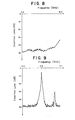
- Figs. 2 and 3 of the accompanying drawings show the insertion loss (in dB) of the filter device of US-A-4 547 754 as a function of the operating frequency (in GHz), and it is apparent that the input/output coupling undesirably increases at frequencies above 4.5 GHz. That is, the device propagates the input signal irrespective of the resonance of the YIG thin film elements, and does not function as a filter.
- a filter of this construction can have a high centre frequency above several GHz as shown in Fig. 4 of the accompanying drawings, which is a plot of isolation (in dB) against frequency (in GHz), but it is suitable only for a fixed band or narrow bandwidth variable filter because of the narrow bandwidth of the high-frequency coupling efficiency and isolation characteristics: a broad band variable filter cannot be realised.
- Fig. 4 shows as a measurement result the isolation characteristics of this filter device for different input frequencies and indicates that an effective filtering function with an isolation of 40 dB or more is accomplished in a narrow band of about three gigahertz between 11.75 and 14.75 GHz.
- a ferromagnetic resonator comprising:
- a ferromagnetic resonator comprising a non-magnetic substrate, a ferrimagnetic thin film element formed on a major surface of said non-magnetic substrate, a strip line electromagnetically coupled to said ferrimagnetic thin film element, a conductive wall of ground potential facing said strip line, and spaced at a predetermined distance therefrom, an end of said strip line being connected to said conductive wall of ground potential, and bias magnetic field means applying a dc magnetic field to said ferrimagnetic thin film perpendicular to said major surface thereof.
- Ferromagnetic resonator embodying the present invention and described hereinbelow are operable at high frequency; and are suitable for use as variable filter devices having a wide frequency band.
- Filter devices embodying the invention are suitable for use in microwave integrated circuits (MI(s).
- Ferromagnetic resonators embodying the invention and described in detail below are of a "short" type having microstrip lines grounded at the ends, and are constructed with the intention of lowering the effective dielectric constant E eff of its transmission system down to almost unity by the utilisation of a so-called suspended substrate strip line configuration or an inverted microstrip line configuration. Fig.
- FIG. 5 shows the structural arrangement of embodiments of this invention, which comprise a device main body 25 including a non-magnetic substrate (for example, a GGG substrate) 21, ferrimagnetic thin film elements (for example, YIG magnetic thin film elements) 22 formed on one main surface of the non-magnetic substrate 21, and strip lines 23 electromagnetically coupled with the ferrimagnetic thin film elements 22, and is further provided with conductive walls 24 which confront the strip lines 23 with a certain spacing formed therebetween and which ground one end of each of the strip lines, and a means 26 for applying a dc bias magnetic field to the ferrimagnetic thin film elements (that is, the YIG magnetic thin film elements) 22, so that transmission lines are formed in the structure of a suspended substrate strip line configuration or an inverted microstrip line configuration.
- a non-magnetic substrate for example, a GGG substrate
- ferrimagnetic thin film elements for example, YIG magnetic thin film elements
- FIG. 5, 6 and 7 show a cross-sectional view, a plan view of the main body 25 and a partially-exploded perspective view of the device, respectively.
- This embodiment employs the suspended substrate strip line structure, and the conductive walls 24 are constructed to form a shielding case which encloses the device main body 25.
- the device main body 25 includes a GGG non-magnetic substrate 21, and its one main surface has first and second YIG magnetic thin film elements 22A and 22B with a certain spacing from each other and a third YIG magnetic thin film element 22C disposed between the YIG elements 22A and 22B for providing the magnetic coupling for them.
- the magnetic thin film elements 22A, 22B and 22C may have a groove in the periphery on one main surface of the magnetic thin film or may have a smaller thickness in the central portion than the peripheral portion so as to suppress a spurious response, as disclosed in the aforementioned US Patent US-A-4 547 754.
- the conductor 27 has sections providing first and second microstrip lines, namely an input strip line 23A and an output strip line 23B disposed parallel to each other and extending across the first and second YIG magnetic thin film elements 22A and 22B, respectively, a central ground pattern 23C located between and parallel to the strip lines 23A and 23B and extending across the third central YIG magnetic thin film element 22C and connected at its opposite ends with the strip lines 23A and 23B, and grounding ends 27A and 27B engaging the grounded surface of part 24B and connecting the strip line 23A to one end of the central ground pattern 23C and the strip line 23B to the other end of the central ground pattern 23C.
- the ground conductive walls 24, which are at ground potential, comprise a first conductive wall section 24A and a second conductive wall section 24B as shown in the partly exploded perspective view of Fig. 7.
- the first conductive wall section 24A has ledges 28A and 28B for supporting the GGG non-magnetic substrate 21 at the ends of the substrate 21 adjacent to the YIG magnetic thin film elements 22A and 22B.
- the ledges 28A and 28B are separated by an interposed recess 29.
- the GGG non-magnetic substrate 21 confronts the inner surface of the conductive wall section 24A with a certain spacing dl being provided by the recess 29.
- the second conductive wall section 24B has recesses 30A and 30B in portions confronting the first and second microstrip lines 23A and 23B, that is, the locations of the first and second YIG magnetic thin film elements 22A and 22B (not shown in Fig. 7).
- the structure is dimensioned such that when the conductive wall sections 24A and 24B are put together with the substrate 21 interleaved therebetween, a protruding section 31 between the recesses 30A and 30B comes into contact with the central ground pattern 23C of the conductive pattern of the conductor 27 so as to establish an electrical connection therebetween, while at the same time the protruding section 31 and the central ground pattern 23C in combination provide isolation between the input and output lines 23A and 23B, and the recesses 30A and 30B provide a certain spacing d2 between the GGG non-magnetic substrate 21 and the confronting inner surfaces of the conductive wall section 24B.
- the dc bias magnetic field application means 26 is constructed in such a way that a pair of cores 32a and 32b have central magnetic poles 32al and 32bl thereof confronting each other and disposed at opposite sides of the device main body 25, with windings 43a and 43b being placed on the respective central magnetic poles 31al and 31bl, so that a dc bias magnetic field is created between the poles.
- the transmission lines are constructed to form a so-called suspended substrate strip line structure, which allows a smaller effective dielectric constant ⁇ eff despite the use of the GGG non-magnetic substrate 21.
- this condition is satisfied up to a frequency as high as 25 GHz for the YIG magnetic thin film elements 22. Accordingly, this structure retains the efficiency of coupling between the input and output lines and the YIG magnetic thin film elements, that is, the YIG resonator, up to such a high frequency, whereby a broadband variable filter operative at high frequencies can be realised.
- the effective dielectric constant ⁇ eff of the microstrip lines with a 50-ohm characteristic impedance is 8.6 for the line on the alumina substrate 2 and 7.3 for the line on the GGG substrate 9.
- the effective dielectric constant ⁇ eff of the 50-ohm microstrip lines is 4.9 for the line on the quartz substrate and 5.1 for the line on the GGG substrate.
- the filter structure embodying the present invention using direct coupling for the YIG resonator, that is, the YIG magnetic thin film elements, enables perfect isolation up to extremely high frequencies owing to the absence of a strip line for linking the resonator elements, and because of the high-frequency isolation between the input and output strip lines provided by the protruding section 31 between the recesses 30A and 30B in the conductive walls 24 and the central ground pattern 23C of the conductive pattern 27, and also the isolation provided by the conductive walls 24 surrounding the device main body 25.
- Fig. 8 is a graph showing the insertion loss plotted against frequency for the filter device described with reference to Figs. 5 to 7, and indicates an isolation of 40 dB or more up to a frequency as high as 17 GHz.
- Fig. 9 shows the characteristics of the filter with a dc bias magnetic field being applied so that the centre frequency is set to 3 GHz. The centre frequency can be varied by adjustment of the magnetic field.
- first and second YIG magnetic thin film elements 22A and 22B can be formed on one main surface of a GGG substrate 21, as shown in Figs. 10 and 11, so that the elements are coupled by a third microstrip line 33 in the same manner as described in connection with Fig. 5.
- the third microstrip line 33 can be formed on a base 24 of polyester film, for example, so that the third microstrip line 33 on the polyester film confronts the first and second YIG magnetic thin film elements 22A and 22B on the GGG non-magnetic substrate 21.
- the third microstrip line 33 may be provided at both of its ends with grounding ends 33A and 33B, which are interposed together with the non-magnetic substrate 21 between the first and second conductive wall sections 24A and 24B and which ends 33A and 33B are in contact with the first conductive wall section 24A of the conductive walls 24 of ground potential.
- the remaining arrangement of Figs. 10 and 11 is common to that of Figs. 5 and 6, and like parts are designated by the same references, so that the explanation thereof need not be repeated.
- This modified arrangement also meets the condition that the YIG magnetic thin film elements are placed in the vicinity of the grounding ends of the strip lines for frequencies up to as high as 25 GHz, and high- efficiency coupling between the strip lines and YIG magnetic thin film elements can be retained.
- the distance from each of two intersections between the first and second microstrip lines 22A and 22B and the third microstrip line 33 to the grounding end becomes equal to Xg/4 at a frequency of 12.5 GHz and, although the frequency with satisfactory isolation is not so high as compared with the arrangement shown in Figs. 5 to 7, a significant improvement is achieved when compared with a conventional filter device.
- the foregoing embodiment is constructed so that the YIG magnetic thin film elements 22 (22A and 22B) are on one surface of the GGG non-magnetic substrate 21 and the conductive pattern 27 such as the first and second strip lines is on the other surface, in an alternative arrangement the conductive pattern 27 is formed on a film made of polyester or the like provided separately from the non-magnetic substrate 21, and then the film with the formation of conductive pattern is placed over the GGG non-magnetic substrate 21.
- FIGs. 12 and 13 show a cross-sectional view and a plan view of the device for the latter case.
- components identical to those shown in Figs. 5 and 6 are designated by common references and an explanation thereof is not repeated.
- the arrangement of Figures 12 and 13 has part of the conductive walls 24, that is, the conductive wall section 24A, removed, and an open wall structure is formed.
- the 50-ohm line has a width of 1.26 mm and an effective dielectric constant f- ef of as small as 1.9. Also in this case, however, when the cores 32a and 32b of the bias magnetic field source are made of material having a shielding effect, the overall structure becomes virtually identical to the suspended substrate microstrip line structure.
- the YIG magnetic thin film elements 22A, 22B and 22C formed on a main surface of the GGG non-magnetic substrate can be produced concurrently by growing an YIG thin film epitaxially on the entire main surface and thereafter patterning the film into the lands by photolithography, so that this embodiment is suitable for volume production.
- the present invention enables a drastic reduction in the effective dielectric constant ⁇ eff of the transmission lines, whereby a filter with a high centre frequency of the order of GHz can be achieved despite the "short" type structure.
- a broadband variable filter having a variable centre frequency from a low frequency to a high frequency of the order of GHz through the provision of a variable bias magnetic field source.
Landscapes
- Control Of Motors That Do Not Use Commutators (AREA)
Abstract
Description
- The invention relates to ferromagnetic resonators and to filter devices utilising ferromagnetic resonance.
- Our US Patent US-A-4 547 754 discloses a filter device utilising a ferrimagnetic thin film of yttrium iron garnet (YIG) formed on a gadolinium-gallium garnet (GGG) substrate by a liquid phase epitaxial (LPE) growth process. Filter devices of this type using YIG thin film elements attract attention for use as microwave integrated circuit (MIC) filters because of the high Q values of their resonance characteristics in the microwave frequency band, compact structure, and suitability for mass production by a selective patterning process by LPE and lithography.
- An MIC band-pass filter using a YIG thin film may be constructed generally as shown in Fig. 1 of the accompanying drawings, for example. A dielectric substrate 1 made of alumina or the like has a first main surface coated with a
ground conductor 2 and has a second main surface coated with first and second microstrip lines disposed in a parallel arrangement to form input andoutput transmission lines strip lines ground conductor 2 by respective connnecting conductors. Ends 3a and 4a of the input andoutput lines thin film elements respective microstrip lines thin film elements GGG substrate 9 by the above-mentioned thin film forming technique and patterning the film into circular lands by a selective etching technique, for example photolithography. Extending between the first and second YIGthin film elements third microstrip line 10 for providing electromagnetic coupling between the elements. Thecoupling transmission line 10 is formed on a second main surface of thesubstrate 9, with both ends of thetransmission line 10 being connected to theground conductor 2 by connectingconductors 11 and 12. - MIC filter devices constructed as described in US-A-4 547 754 are restricted to relatively low centre frequencies of at most several GHz due to two major reasons that will now be explained. The first reason is that the YIG thin film elements need to be placed at positions where the magnetic field is maximum for the purpose of magnetic coupling with each microstrip line. However, this condition is not met for relatively high centre frequencies. In particular, the magnetic field is maximum at the grounding end of the microstrip line and minimum at a position λg/4 (where Xg is the propagation wavelength) away from the maximum position. Therefore, each YIG thin film element needs to be disposed as near to the grounding end of the microstrip line as possible for good coupling at relatively high centre frequencies. The propagation wavelength λg is expressed in terms of the effective dielectric constant εeff, determined from the dielectric constants of the dielectric substrate 1 and
GGG substrate 9 and the shape of the microstrip lines, as -

- With the intention of overcoming the above-mentioned deficiencies, we have proposed in Japanese Patent Application 59-187079 a filter device in which the microstrip lines each have one of their ends open with YIG
thin film elements - A filter of this construction can have a high centre frequency above several GHz as shown in Fig. 4 of the accompanying drawings, which is a plot of isolation (in dB) against frequency (in GHz), but it is suitable only for a fixed band or narrow bandwidth variable filter because of the narrow bandwidth of the high-frequency coupling efficiency and isolation characteristics: a broad band variable filter cannot be realised. Fig. 4 shows as a measurement result the isolation characteristics of this filter device for different input frequencies and indicates that an effective filtering function with an isolation of 40 dB or more is accomplished in a narrow band of about three gigahertz between 11.75 and 14.75 GHz.
- According to a first aspect of the invention there is provided a ferromagnetic resonator comprising:
- a non-magnetic substrate,
- a ferrimagnetic thin film element formed on a major surface of the non-magnetic substrate,
- a strip line disposed at another major surface of the non-magnetic substrate and electromagnetically coupled to the ferrimagnetic thin film element,
- a conductive wall connected or connectable to ground potential, the wall facing the strip line and being spaced at a predetermined distance therefrom,
- an end of the strip line being connected to the conductive wall, and bias magnetic field means for applying a dc magnetic field to the ferrimagnetic thin film element perpendicular to the major surface thereof.
- According to a second aspect of the present invention there is provided a ferromagnetic resonator comprising a non-magnetic substrate, a ferrimagnetic thin film element formed on a major surface of said non-magnetic substrate, a strip line electromagnetically coupled to said ferrimagnetic thin film element, a conductive wall of ground potential facing said strip line, and spaced at a predetermined distance therefrom, an end of said strip line being connected to said conductive wall of ground potential, and bias magnetic field means applying a dc magnetic field to said ferrimagnetic thin film perpendicular to said major surface thereof.
- Ferromagnetic resonator embodying the present invention and described hereinbelow are operable at high frequency; and are suitable for use as variable filter devices having a wide frequency band.
- Filter devices embodying the invention are suitable for use in microwave integrated circuits (MI(s).
- The invention will now be further described, by way of illustrative and non-limiting example, with reference to the accompanying drawings, in which:
- Fig. 1 is a perspective view of a filter device utilising ferromagnetic resonance and having input and output microstrip lines constructed as described in US Patent US-A-4 547 754;
- Figs. 2 and 3 are characteristic graphs showing insertion loss as a function of input frequency for the filter device of US Patent US-A-4 547 754;
- Fig. 4 is a plot of the isolation provided by the above-described modified filter device wherein YIG discs are provided at positions distant from open ends by an odd multiple of λg/4 as a function of input frequency;
- Figs. 5, 6 and 7 are structural views of a ferromagnetic resonator embodying the present invention;
- Figs. 8 and 9 are characteristic graphs for the resonator of Figs. 5, 6 and 7; and
- Figs. 10, 11, 12 and 13 are structural views used to explain other embodiments of this invention.
- Ferromagnetic resonators embodying the invention and described in detail below are of a "short" type having microstrip lines grounded at the ends, and are constructed with the intention of lowering the effective dielectric constant E eff of its transmission system down to almost unity by the utilisation of a so-called suspended substrate strip line configuration or an inverted microstrip line configuration. Fig. 5 shows the structural arrangement of embodiments of this invention, which comprise a device
main body 25 including a non-magnetic substrate (for example, a GGG substrate) 21, ferrimagnetic thin film elements (for example, YIG magnetic thin film elements) 22 formed on one main surface of thenon-magnetic substrate 21, andstrip lines 23 electromagnetically coupled with the ferrimagneticthin film elements 22, and is further provided withconductive walls 24 which confront thestrip lines 23 with a certain spacing formed therebetween and which ground one end of each of the strip lines, and ameans 26 for applying a dc bias magnetic field to the ferrimagnetic thin film elements (that is, the YIG magnetic thin film elements) 22, so that transmission lines are formed in the structure of a suspended substrate strip line configuration or an inverted microstrip line configuration. - A first embodiment of this invention will now be described in more detail with reference to Figs. 5, 6 and 7, which show a cross-sectional view, a plan view of the
main body 25 and a partially-exploded perspective view of the device, respectively. This embodiment employs the suspended substrate strip line structure, and theconductive walls 24 are constructed to form a shielding case which encloses the devicemain body 25. The devicemain body 25 includes a GGGnon-magnetic substrate 21, and its one main surface has first and second YIG magneticthin film elements thin film element 22C disposed between theYIG elements thin film elements non-magnetic substrate 21 opposite to that where the YIG magneticthin film elements conductor 27. Theconductor 27 has sections providing first and second microstrip lines, namely aninput strip line 23A and anoutput strip line 23B disposed parallel to each other and extending across the first and second YIG magneticthin film elements central ground pattern 23C located between and parallel to thestrip lines thin film element 22C and connected at its opposite ends with thestrip lines grounding ends part 24B and connecting thestrip line 23A to one end of thecentral ground pattern 23C and thestrip line 23B to the other end of thecentral ground pattern 23C. - The ground
conductive walls 24, which are at ground potential, comprise a firstconductive wall section 24A and a secondconductive wall section 24B as shown in the partly exploded perspective view of Fig. 7. The firstconductive wall section 24A has ledges 28A and 28B for supporting the GGGnon-magnetic substrate 21 at the ends of thesubstrate 21 adjacent to the YIG magneticthin film elements recess 29. By being placed on the ledges 28A and 28B, the GGGnon-magnetic substrate 21 confronts the inner surface of theconductive wall section 24A with a certain spacing dl being provided by therecess 29. The secondconductive wall section 24B has recesses 30A and 30B in portions confronting the first andsecond microstrip lines thin film elements conductive wall sections substrate 21 interleaved therebetween, aprotruding section 31 between therecesses central ground pattern 23C of the conductive pattern of theconductor 27 so as to establish an electrical connection therebetween, while at the same time theprotruding section 31 and thecentral ground pattern 23C in combination provide isolation between the input andoutput lines recesses non-magnetic substrate 21 and the confronting inner surfaces of theconductive wall section 24B. - The dc bias magnetic field application means 26 is constructed in such a way that a pair of
cores main body 25, withwindings - According to the resonator structure described above, the transmission lines are constructed to form a so-called suspended substrate strip line structure, which allows a smaller effective dielectric constant εeff despite the use of the GGG
non-magnetic substrate 21. Typically, using a GGG substrate of 0.4mm in thickness for thenon-magnetic substrate 21, with spacings dl and d2 of 0.6mm each being provided between the upper and lower surfaces of theGGG substrate 21 and theconductive walls 24, an effective dielectric constant of 2.2 is achieved for a 50-ohm strip line which is 1.25mm in width. When the YIG magneticthin film elements grounding ends strip lines thin film elements 22. Accordingly, this structure retains the efficiency of coupling between the input and output lines and the YIG magnetic thin film elements, that is, the YIG resonator, up to such a high frequency, whereby a broadband variable filter operative at high frequencies can be realised. - The filter device described in connection with Fig. 1 uses a
GGG substrate 9 of high dielectric constant Er = 13, and therefore, even by the combinational use of a dielectric substrate 1 having a small dielectric constant, the effective dielectric constant εeff cannot be made sufficiently small. For example, using an alumina sheet of 1.27mm in thickness (εr = 10) as a dielectric substrate 1 and aGGG substrate 9 which is 0.4mm in thickness, the effective dielectric constant εeff of the microstrip lines with a 50-ohm characteristic impedance is 8.6 for the line on thealumina substrate 2 and 7.3 for the line on theGGG substrate 9. In another example using a quartz substrate (E = 3.8) which is 0.5mm in thickness as a dielectric substrate 1 and aGGG substrate 9 which is 0.4mm in thickness, the effective dielectric constant εeff of the 50-ohm microstrip lines is 4.9 for the line on the quartz substrate and 5.1 for the line on the GGG substrate. - The filter structure embodying the present invention, using direct coupling for the YIG resonator, that is, the YIG magnetic thin film elements, enables perfect isolation up to extremely high frequencies owing to the absence of a strip line for linking the resonator elements, and because of the high-frequency isolation between the input and output strip lines provided by the protruding
section 31 between therecesses conductive walls 24 and thecentral ground pattern 23C of theconductive pattern 27, and also the isolation provided by theconductive walls 24 surrounding the devicemain body 25. - Fig. 8 is a graph showing the insertion loss plotted against frequency for the filter device described with reference to Figs. 5 to 7, and indicates an isolation of 40 dB or more up to a frequency as high as 17 GHz. Fig. 9 shows the characteristics of the filter with a dc bias magnetic field being applied so that the centre frequency is set to 3 GHz. The centre frequency can be varied by adjustment of the magnetic field.
- Although the foregoing embodiment employs direct coupling for the YIG resonator, the present invention is not limited to this. Alternatively, for example, first and second YIG magnetic
thin film elements GGG substrate 21, as shown in Figs. 10 and 11, so that the elements are coupled by athird microstrip line 33 in the same manner as described in connection with Fig. 5. In this case, thethird microstrip line 33 can be formed on abase 24 of polyester film, for example, so that thethird microstrip line 33 on the polyester film confronts the first and second YIG magneticthin film elements non-magnetic substrate 21. Thethird microstrip line 33 may be provided at both of its ends with grounding ends 33A and 33B, which are interposed together with thenon-magnetic substrate 21 between the first and secondconductive wall sections conductive wall section 24A of theconductive walls 24 of ground potential. The remaining arrangement of Figs. 10 and 11 is common to that of Figs. 5 and 6, and like parts are designated by the same references, so that the explanation thereof need not be repeated. - This modified arrangement also meets the condition that the YIG magnetic thin film elements are placed in the vicinity of the grounding ends of the strip lines for frequencies up to as high as 25 GHz, and high- efficiency coupling between the strip lines and YIG magnetic thin film elements can be retained. The distance from each of two intersections between the first and
second microstrip lines third microstrip line 33 to the grounding end becomes equal to Xg/4 at a frequency of 12.5 GHz and, although the frequency with satisfactory isolation is not so high as compared with the arrangement shown in Figs. 5 to 7, a significant improvement is achieved when compared with a conventional filter device. - Although the foregoing embodiment is constructed so that the YIG magnetic thin film elements 22 (22A and 22B) are on one surface of the GGG
non-magnetic substrate 21 and theconductive pattern 27 such as the first and second strip lines is on the other surface, in an alternative arrangement theconductive pattern 27 is formed on a film made of polyester or the like provided separately from thenon-magnetic substrate 21, and then the film with the formation of conductive pattern is placed over the GGGnon-magnetic substrate 21. - Although the above-described embodiments employ a suspended substrate strip line structure, the present invention can be applied equally to the inverted microstrip line structure. Figs. 12 and 13 show a cross-sectional view and a plan view of the device for the latter case. In Figures 12 and 13, components identical to those shown in Figs. 5 and 6 are designated by common references and an explanation thereof is not repeated. The arrangement of Figures 12 and 13 has part of the
conductive walls 24, that is, theconductive wall section 24A, removed, and an open wall structure is formed. - In this structure, with a spacing of 0.4mm produced by the
recesses conductive walls 24 with respect to the surface of the GGGnon-magnetic substrate 21 on the side of the microstrip line, the 50-ohm line has a width of 1.26 mm and an effective dielectric constant f- ef of as small as 1.9. Also in this case, however, when thecores - The YIG magnetic
thin film elements - As described above, the present invention enables a drastic reduction in the effective dielectric constant εeff of the transmission lines, whereby a filter with a high centre frequency of the order of GHz can be achieved despite the "short" type structure.
- It is also possible to construct a broadband variable filter having a variable centre frequency from a low frequency to a high frequency of the order of GHz through the provision of a variable bias magnetic field source.
Claims (2)
Applications Claiming Priority (2)
| Application Number | Priority Date | Filing Date | Title |
|---|---|---|---|
| JP60065874A JPS61224702A (en) | 1985-03-29 | 1985-03-29 | Ferromagnetic resonator |
| JP65874/85 | 1985-03-29 |
Publications (3)
| Publication Number | Publication Date |
|---|---|
| EP0196918A2 true EP0196918A2 (en) | 1986-10-08 |
| EP0196918A3 EP0196918A3 (en) | 1988-08-17 |
| EP0196918B1 EP0196918B1 (en) | 1992-01-15 |
Family
ID=13299558
Family Applications (1)
| Application Number | Title | Priority Date | Filing Date |
|---|---|---|---|
| EP86302421A Expired - Lifetime EP0196918B1 (en) | 1985-03-29 | 1986-04-01 | Ferromagnetic resonators |
Country Status (5)
| Country | Link |
|---|---|
| US (1) | US4679015A (en) |
| EP (1) | EP0196918B1 (en) |
| JP (1) | JPS61224702A (en) |
| CA (1) | CA1248187A (en) |
| DE (1) | DE3683387D1 (en) |
Cited By (2)
| Publication number | Priority date | Publication date | Assignee | Title |
|---|---|---|---|---|
| DE3740376A1 (en) * | 1986-11-28 | 1988-06-01 | Sony Corp | TUNED FILM FILTER WITH FERROMAGNETIC RESONANCE |
| DE3923209A1 (en) * | 1988-07-20 | 1990-01-25 | Hitachi Ltd | MAGNETOSTATIC BAND PASS FILTER |
Families Citing this family (11)
| Publication number | Priority date | Publication date | Assignee | Title |
|---|---|---|---|---|
| US4983936A (en) * | 1986-07-02 | 1991-01-08 | Sony Corporation | Ferromagnetic resonance device |
| JPS63103501A (en) * | 1986-10-20 | 1988-05-09 | Sony Corp | Ferromagnetic resonator |
| JPS6392403U (en) * | 1986-12-05 | 1988-06-15 | ||
| JPH0812966B2 (en) * | 1987-11-17 | 1996-02-07 | 三菱電機株式会社 | Ferrimagnetic thin film resonator |
| US4998080A (en) * | 1989-06-02 | 1991-03-05 | Polytechnic University | Microwave channelizer based on coupled YIG resonators |
| US5424698A (en) * | 1993-12-06 | 1995-06-13 | Motorola, Inc. | Ferrite-semiconductor resonator and filter |
| US5677652A (en) * | 1996-04-24 | 1997-10-14 | Verticom, Inc. | Microwave ferrite resonator with parallel permanent magnet bias |
| CN1123946C (en) * | 1997-07-24 | 2003-10-08 | Tdk株式会社 | Magnetostatic wave device |
| WO2002031522A1 (en) * | 2000-10-09 | 2002-04-18 | Regents Of The University Of Minnesota | Method and apparatus for magnetic resonance imaging and spectroscopy using microstrip transmission line coils |
| CN114914647B (en) * | 2022-05-17 | 2023-04-28 | 电子科技大学 | Tunable broadband band-stop filter based on ferrite material |
| CN118399046B (en) * | 2024-06-26 | 2024-09-03 | 成都威频科技有限公司 | A low frequency narrow band YIG bandpass filter |
Family Cites Families (2)
| Publication number | Priority date | Publication date | Assignee | Title |
|---|---|---|---|---|
| US4197517A (en) * | 1978-11-03 | 1980-04-08 | The United States Of America As Represented By The Secretary Of The Navy | High speed frequency tunable microwave filter |
| CA1204181A (en) * | 1982-12-06 | 1986-05-06 | Yoshikazu Murakami | Ferromagnetic resonator |
-
1985
- 1985-03-29 JP JP60065874A patent/JPS61224702A/en active Granted
-
1986
- 1986-03-27 CA CA000505320A patent/CA1248187A/en not_active Expired
- 1986-03-27 US US06/844,984 patent/US4679015A/en not_active Expired - Fee Related
- 1986-04-01 DE DE8686302421T patent/DE3683387D1/en not_active Expired - Lifetime
- 1986-04-01 EP EP86302421A patent/EP0196918B1/en not_active Expired - Lifetime
Cited By (4)
| Publication number | Priority date | Publication date | Assignee | Title |
|---|---|---|---|---|
| DE3740376A1 (en) * | 1986-11-28 | 1988-06-01 | Sony Corp | TUNED FILM FILTER WITH FERROMAGNETIC RESONANCE |
| FR2607640A1 (en) * | 1986-11-28 | 1988-06-03 | Sony Corp | FILTER GIVES THIN FILES |
| US4945324A (en) * | 1986-11-28 | 1990-07-31 | Sony Corporation | Thin film ferromagnetic resonance tuned filter |
| DE3923209A1 (en) * | 1988-07-20 | 1990-01-25 | Hitachi Ltd | MAGNETOSTATIC BAND PASS FILTER |
Also Published As
| Publication number | Publication date |
|---|---|
| JPS61224702A (en) | 1986-10-06 |
| EP0196918A3 (en) | 1988-08-17 |
| EP0196918B1 (en) | 1992-01-15 |
| US4679015A (en) | 1987-07-07 |
| DE3683387D1 (en) | 1992-02-27 |
| CA1248187A (en) | 1989-01-03 |
| JPH0575202B2 (en) | 1993-10-20 |
Similar Documents
| Publication | Publication Date | Title |
|---|---|---|
| CA2249489C (en) | High-frequency transmission line, dielectric resonator, filter, duplexer, and communication device | |
| CA2063119C (en) | Miniature dual mode planar filters | |
| US3732508A (en) | Strip line to waveguide transition | |
| JP3409729B2 (en) | Dielectric resonator device, duplexer and communication device | |
| US3740675A (en) | Yig filter having a single substrate with all transmission line means located on a common surface thereof | |
| US6538527B2 (en) | Resonator, filter, duplexer, and communication device | |
| EP0196918B1 (en) | Ferromagnetic resonators | |
| US3904997A (en) | Trapped-radiation microwave transmission line | |
| GB2131628A (en) | Magnetically tuned resonant circuit | |
| GB2371415A (en) | Filter, multiplexer and communication apparatus | |
| US4521753A (en) | Tuned resonant circuit utilizing a ferromagnetically coupled interstage line | |
| US3831114A (en) | Encapsulated microstrip circulator with mode elimination means | |
| JP4105017B2 (en) | Waveguide type dielectric filter | |
| US7183874B2 (en) | Casing contained filter | |
| JP2630387B2 (en) | Dielectric filter | |
| JPH0465562B2 (en) | ||
| US4871988A (en) | Microwave transmission line of the symmetrical type and with two coplanar conductors | |
| GB2345583A (en) | Coplanar rail line transmission line | |
| KR100396922B1 (en) | Magnetostatic Wave Filter | |
| CA1277377C (en) | Ferrimagnetic resonator device | |
| JPH0577201B2 (en) | ||
| JPH07105646B2 (en) | Ferromagnetic thin film filter | |
| JPH0328563Y2 (en) | ||
| JPS6165502A (en) | Ferromagnetic thin film filter | |
| JPH0258401A (en) | Ferrimagnetic thin film filter |
Legal Events
| Date | Code | Title | Description |
|---|---|---|---|
| PUAI | Public reference made under article 153(3) epc to a published international application that has entered the european phase |
Free format text: ORIGINAL CODE: 0009012 |
|
| AK | Designated contracting states |
Kind code of ref document: A2 Designated state(s): DE FR GB NL |
|
| PUAL | Search report despatched |
Free format text: ORIGINAL CODE: 0009013 |
|
| AK | Designated contracting states |
Kind code of ref document: A3 Designated state(s): DE FR GB NL |
|
| 17P | Request for examination filed |
Effective date: 19890120 |
|
| 17Q | First examination report despatched |
Effective date: 19910104 |
|
| GRAA | (expected) grant |
Free format text: ORIGINAL CODE: 0009210 |
|
| AK | Designated contracting states |
Kind code of ref document: B1 Designated state(s): DE FR GB NL |
|
| REF | Corresponds to: |
Ref document number: 3683387 Country of ref document: DE Date of ref document: 19920227 |
|
| ET | Fr: translation filed | ||
| PLBE | No opposition filed within time limit |
Free format text: ORIGINAL CODE: 0009261 |
|
| STAA | Information on the status of an ep patent application or granted ep patent |
Free format text: STATUS: NO OPPOSITION FILED WITHIN TIME LIMIT |
|
| 26N | No opposition filed | ||
| PGFP | Annual fee paid to national office [announced via postgrant information from national office to epo] |
Ref country code: GB Payment date: 19970324 Year of fee payment: 12 |
|
| PGFP | Annual fee paid to national office [announced via postgrant information from national office to epo] |
Ref country code: FR Payment date: 19970409 Year of fee payment: 12 |
|
| PGFP | Annual fee paid to national office [announced via postgrant information from national office to epo] |
Ref country code: NL Payment date: 19970428 Year of fee payment: 12 |
|
| PG25 | Lapsed in a contracting state [announced via postgrant information from national office to epo] |
Ref country code: GB Free format text: LAPSE BECAUSE OF NON-PAYMENT OF DUE FEES Effective date: 19980401 |
|
| PG25 | Lapsed in a contracting state [announced via postgrant information from national office to epo] |
Ref country code: FR Free format text: THE PATENT HAS BEEN ANNULLED BY A DECISION OF A NATIONAL AUTHORITY Effective date: 19980430 |
|
| PG25 | Lapsed in a contracting state [announced via postgrant information from national office to epo] |
Ref country code: NL Free format text: LAPSE BECAUSE OF NON-PAYMENT OF DUE FEES Effective date: 19981101 |
|
| GBPC | Gb: european patent ceased through non-payment of renewal fee |
Effective date: 19980401 |
|
| NLV4 | Nl: lapsed or anulled due to non-payment of the annual fee |
Effective date: 19981101 |
|
| REG | Reference to a national code |
Ref country code: FR Ref legal event code: ST |
|
| PGFP | Annual fee paid to national office [announced via postgrant information from national office to epo] |
Ref country code: DE Payment date: 20030409 Year of fee payment: 18 |
|
| PG25 | Lapsed in a contracting state [announced via postgrant information from national office to epo] |
Ref country code: DE Free format text: LAPSE BECAUSE OF NON-PAYMENT OF DUE FEES Effective date: 20041103 |