EP0196875A1 - Optical component mounting - Google Patents
Optical component mounting Download PDFInfo
- Publication number
- EP0196875A1 EP0196875A1 EP86302258A EP86302258A EP0196875A1 EP 0196875 A1 EP0196875 A1 EP 0196875A1 EP 86302258 A EP86302258 A EP 86302258A EP 86302258 A EP86302258 A EP 86302258A EP 0196875 A1 EP0196875 A1 EP 0196875A1
- Authority
- EP
- European Patent Office
- Prior art keywords
- component
- optical
- fibre
- heating means
- solder
- Prior art date
- Legal status (The legal status is an assumption and is not a legal conclusion. Google has not performed a legal analysis and makes no representation as to the accuracy of the status listed.)
- Granted
Links
Images


Classifications
-
- G—PHYSICS
- G02—OPTICS
- G02B—OPTICAL ELEMENTS, SYSTEMS OR APPARATUS
- G02B6/00—Light guides; Structural details of arrangements comprising light guides and other optical elements, e.g. couplings
- G02B6/24—Coupling light guides
- G02B6/42—Coupling light guides with opto-electronic elements
- G02B6/4201—Packages, e.g. shape, construction, internal or external details
- G02B6/4219—Mechanical fixtures for holding or positioning the elements relative to each other in the couplings; Alignment methods for the elements, e.g. measuring or observing methods especially used therefor
- G02B6/4236—Fixing or mounting methods of the aligned elements
- G02B6/4238—Soldering
-
- G—PHYSICS
- G02—OPTICS
- G02B—OPTICAL ELEMENTS, SYSTEMS OR APPARATUS
- G02B6/00—Light guides; Structural details of arrangements comprising light guides and other optical elements, e.g. couplings
- G02B6/24—Coupling light guides
- G02B6/42—Coupling light guides with opto-electronic elements
- G02B6/4201—Packages, e.g. shape, construction, internal or external details
- G02B6/4219—Mechanical fixtures for holding or positioning the elements relative to each other in the couplings; Alignment methods for the elements, e.g. measuring or observing methods especially used therefor
- G02B6/422—Active alignment, i.e. moving the elements in response to the detected degree of coupling or position of the elements
- G02B6/4226—Positioning means for moving the elements into alignment, e.g. alignment screws, deformation of the mount
-
- H—ELECTRICITY
- H05—ELECTRIC TECHNIQUES NOT OTHERWISE PROVIDED FOR
- H05K—PRINTED CIRCUITS; CASINGS OR CONSTRUCTIONAL DETAILS OF ELECTRIC APPARATUS; MANUFACTURE OF ASSEMBLAGES OF ELECTRICAL COMPONENTS
- H05K3/00—Apparatus or processes for manufacturing printed circuits
- H05K3/30—Assembling printed circuits with electric components, e.g. with resistors
- H05K3/32—Assembling printed circuits with electric components, e.g. with resistors electrically connecting electric components or wires to printed circuits
- H05K3/34—Assembling printed circuits with electric components, e.g. with resistors electrically connecting electric components or wires to printed circuits by soldering
- H05K3/3494—Heating processes for reflow soldering
Definitions
- This invention relates to optical components and methods of mounting optical components.
- the invention has an important application in the field of assembling optical devices for optical communication systems.
- a method of mounting an optical component on a substrate comprising providing a component with dedicated heating means and fixing the component to the substrate with solder, wherein the component and solder are heated locally by the dedicated heating means.
- the temperature of the heating means is electrically controlled.
- the heating means comprises a resistive heating element.
- the heating means may be provided by bonding or otherwise affixing a miniature resistor to the component.
- the heating means may be provided by deposition of a resistive ink film on a suitably insulated surface on the component.
- the insulated surface may be a ceramic layer.
- Metallised contacts may be provided to allow simple electrical connection to the resistive film.
- an optical component comprises dedicated heating means to facilitate solder mounting of the component.
- the heating means may be a resistive ink film deposited on an insulating surface on the component, and the resistive film may have metallised contacts for electrical connections.
- Figure 1 shows an optical fibre 10 attached to a carrier plate 12, forming an optical fibre carrier assembly 1.
- a laser submount 2 comprises a semiconductor laser 13, mounted on a copper submount 14.
- Such a submount may typically have dimensions of approximately 6mm x 4mm x 1.5mm.
- a groove 15 is provided in the submount 14 so that solder 17 used to fix the fibre carrier assembly onto the stage 16 of submount 14 is prevented from contacting the laser 13.
- solder 17 which may be in the form of a preform or solder paste, is then applied to the stage 16.
- the fibre end 11 must next be optically aligned with the emitting area of the laser 13. Conventionally, this is done by operating the laser under low duty-cycle pulsed conditions, and manipulating the fibre carrier so as to maximise the optical power coupled into the fibre.
- a sophisticated detector 19 must be provided to monitor the light which emerges (in the direction arrowed) from the remote end 18 of the fibre 10. The alignment position is optimal where the power of the transmitted light is a maximum.
- FIG. 2 shows a fibre carrier assembly 3, modified in accordance with the invention to incorporate a suitable heating element 20 as heating means.
- the heating element shown is a so-called chip resistor.
- Chip resistors of this form are commercially available, and comprise a ceramic substrate 21, with a layer of resistive ink 22 deposited on one face. Electrical contact is made via the metallised contacts 23 on each end.
- the ink is usually covered with an electrically insulating glaze.
- An additional metallic surface (not shown), isolated from the ink, may also be provided so that the resistor can be attached to the component with a suitable high temperature solder prior to mounting. Alternatively, where appropriate, the resistor may be attached by fusing a glass frit, for example.
- the chip resistor is usually attached with its resistive face next to the carrier plate 12 for best heat conduction.
- Resistance values for the chip resistor of between 1 and 10 ohms have been found particularly convenient for use according to the present invention.
- the modified fibre carrier assembly 3 which forms the optical component to be fixed, is gripped in a clamp 30, and held over the laser submount 2.
- the clamp 30 grips the metallised ends 23 of the chip resistor 20, and also in this case performs the additional function of allowing electrical contact to be made with the resistor.
- This may be by way of special conductive paths 31, as illustrated, or alternatively, the two jaws of such a clamp, suitably insulated from one another may be direct electrical conductors themselves.
- the submount may be placed on a heating platform (not shown), and its temperature raised, this time to just below the solder melting point. The incremental heat which the dedicated heating element 20 will need to supply is thereby reduced. Potentially damaging stresses induced by differential thermal contraction between submount 14 and fibre carrier 3 on cooling are also thereby limited.
- the carrier assembly 3 is then lowered onto the solder 17.
- the heat from the chip resistor then melts the solder locally.
- the solder conducts heat away from the fibre carrier, and to achieve even the very localised melting needed for mounting by this method, it is normally necessary to increase the current through the resistor at this stage.
- any current changes must be made with care to avoid burning out the resistor, for example, as the rate of thermal dissipation alters.
- Precise control and monitoring of the component temperature is therefore desirable, and may be achieved by a method which is described later.
- the fibre may then be moved to obtain the required correct alignment of fibre end 11 with the lasing facet of the laser 13. Alignment may be made either by using a conventional technique or, when appropriate, the improved method explained in detail below.
- the current through the heating element 20 is then reduced to allow the solder 17 to solidify and fix the fibre and carrier 3 onto the submount.
- the component may then be released from the clamp 30 and the temperature of the heating platform, if used, returned to normal.
- each component could be mounted in like fashion. In this event, the substrate background temperature, being below the solder melting point, need not be lowered to normal until all of the components were mounted.
- the invention has been described, by way of example, with reference to mounting an optical fibre carrier assembly on a laser submount, the invention in its main aspects has general application, both to the modification of other optical components, for example lenses, and to the mounting of such appropriately adapted optical components.
- the heating element shown as a chip resistor in the above example, may also be provided in alternative forms.
- a layer of conductive ink or other conductive material could be printed directly onto a suitably insulated component surface. Such insulation would be essential where the body of the component (eg.
- fibre carrier might otherwise short circuit the heating element current path.
- the printing of such layers onto substrates may be done by the same methods as are used in the fabrication of thick film hybrid circuits or chip resistors.
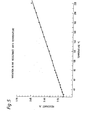
- FIG. 5 is a graph of the variation of resistance with temperature of an ink film resistor of the type described in the foregoing discussion. Of course, if preferred, resistors having a greater thermal variation of resistance than that shown could be used.
- an improved alignment method disclosed below eliminates the requirement to pulse the laser at all, thus substantially reducing the risk of damage.
- More advanced semiconductor lasers now being produced generally incorporate means of current confinement in their structures to enhance the lasing performance.
- such lasers are also only sensitive to injected light, which may induce a photocurrent in a passive (ie. not lasing) laser, in the immediate vicinity of the emitting region of the laser facet.
- the area of maximum photosensitivity may thus conveniently coincide or be close to the area of maximum lasing output. This property may therefore allow laser to fibre alignment to be achieved at high temperatures without the need to pulse drive the laser.
- this may be done by making preliminary measurements at room temperature, before starting the mounting procedure, when the laser can lase without detriment, and any offset between lasing and photocurrent maxima can be easily determined. Subsequently, during the mounting process, the offset is taken into account and the fibre fixed with a corresponding displacement from the photocurrent maximum.
Landscapes
- Physics & Mathematics (AREA)
- General Physics & Mathematics (AREA)
- Optics & Photonics (AREA)
- Optical Couplings Of Light Guides (AREA)
- Mounting And Adjusting Of Optical Elements (AREA)
- Led Device Packages (AREA)
- Mechanical Coupling Of Light Guides (AREA)
- Semiconductor Lasers (AREA)
Abstract
Description
- This invention relates to optical components and methods of mounting optical components. The invention has an important application in the field of assembling optical devices for optical communication systems.
- The importance of achieving accurate mutual alignment of individual components in any optical system is well known. The miniature dimensions of components used in modern optical communication systems render such alignment very difficult both to achieve and to maintain. For example, one of the main problems in the construction of semiconductor laser transmitters is that of efficiently coupling the optical power from a semiconductor laser diode into a monomode fibre. To obtain efficient coupling, the fibre end must be very precisely aligned with the emitting area of the laser facet. When such alignment is achieved, the fibre must then be fixed in place, ideally by a method which ensures that alignment is sustained throughout the device lifetime.
- In the past various methods of mounting have been proposed or employed in an effort to meet the required demands of accuracy and longevity of alignment. Traditionally, components have been fixed by soldering. However, where a number of separate components are to be mounted on the same substrate a series of solders must usually be used, with each successive component being fixed with a progressively lower melting point solder. The first mounted components are not then loosened when others are fixed subsequently. Nevertheless, there are obvious problems if it is necessary, for maintainance purposes, for example, to remove a first mounted component, fixed with a high melting point solder, without disturbing those later mounted components, fixed with lower melting point solders.
- Some methods of restricting the applied soldering heat to the immediate locality of a component have been tried in an attempt to avoid the problems involved in the use of a series of solders. Such methods include the use of a hot gas jet, or direct thermal conduction from a heated clamp. However, because of drawbacks including difficulties in ensuring adequate heat transfer and, more significantly, the difficulty of avoiding alignment perturbations, these techniques have generally proved unsatisfactory, even for laboratory applications.
- The adoption of organic adhesives has been successful for fixing some components, but such adhesives are not generally acceptable for several reasons. Firstly/component replacement is considered difficult, if not wholly impractical. Secondly, during ageing, adhesives may be subject to shrinkage, with the likelihood of adverse consequences on component alignment. Thirdly, also with ageing, adhesives are liable to outgas undesirable organic substances. Enclosed in component packages, such as, for example, a laser transmitter, these substances can cause severe degradation and premature failure of the components.
- It is one object of the present invention to provide a method of mounting optical components, which permits some of the above disadvantages to be overcome or mitigated.
- It is a second object of the present invention to provide an improved optical component adapted to facilitate mounting by the improved method.
- According to the present invention there is provided a method of mounting an optical component on a substrate, the method comprising providing a component with dedicated heating means and fixing the component to the substrate with solder, wherein the component and solder are heated locally by the dedicated heating means.
- Preferably the temperature of the heating means is electrically controlled.
- Conveniently, the heating means comprises a resistive heating element.
- The heating means may be provided by bonding or otherwise affixing a miniature resistor to the component.
- Alternatively, the heating means may be provided by deposition of a resistive ink film on a suitably insulated surface on the component. The insulated surface may be a ceramic layer. Metallised contacts may be provided to allow simple electrical connection to the resistive film.
- According to a second aspect of the present invention, an optical component comprises dedicated heating means to facilitate solder mounting of the component.
- The heating means may be a resistive ink film deposited on an insulating surface on the component, and the resistive film may have metallised contacts for electrical connections.
- The present invention will now be described by way of example and with reference to the accompanying drawings, in which;
- Figure 1 is a schematic illustration of the prior art, showing an optical fibre carrier, conventionally prepared and mounted on a semiconductor laser submount.
- Figure 2 shows schematically an optical fibre carrier adapted according to the second aspect of the present invention. The inset illustrates a resistive heating element which forms the heating means.
- Figure 3 illustrates schematically the mounting of the modified carrier onto a laser submount by a method according to the present invention.
- Figure 4 shows, again in schematic, the final arrangement after mounting.
- Figure 5 is a graph of the change in resistance with temperature of a heating element (of the type shown in the Figure 2 inset).
- A conventional method of mounting will first be described with reference to Figure 1. The mounting of an optical fibre carrier on a semiconductor laser submount is taken as an example.
- Figure 1 shows an
optical fibre 10 attached to acarrier plate 12, forming an optical fibre carrier assembly 1. Alaser submount 2 comprises asemiconductor laser 13, mounted on acopper submount 14. Such a submount may typically have dimensions of approximately 6mm x 4mm x 1.5mm. - A
groove 15 is provided in thesubmount 14 so thatsolder 17 used to fix the fibre carrier assembly onto thestage 16 ofsubmount 14 is prevented from contacting thelaser 13. - During the mounting process the
submount assembly 2 is placed on a temperature controlled heating platform (not shown) and its temperature is raised to slightly above the melting point of the solder to be used. (For normal indium-based solder, this temperature is around 118*C.)Solder 17, which may be in the form of a preform or solder paste, is then applied to thestage 16. The fibre carrier assembly 1, held in a clamp attached to a precision manipulator stack (not shown), is then lowered onto the molten solder. - The fibre end 11 must next be optically aligned with the emitting area of the
laser 13. Conventionally, this is done by operating the laser under low duty-cycle pulsed conditions, and manipulating the fibre carrier so as to maximise the optical power coupled into the fibre. Asophisticated detector 19 must be provided to monitor the light which emerges (in the direction arrowed) from theremote end 18 of thefibre 10. The alignment position is optimal where the power of the transmitted light is a maximum. - When the fibre is in alignment with the laser, the temperature of the heating platform is lowered to allow the solder to solidify and so fix the fibre in position. Finally, the fibre carrier assembly 1 can be released from its clamp (not shown). The completed arrangment is then as illustrated in Figure 1.
- Component modification and mounting according to the present invention will now be described, also with regard to the mounting of an optical fibre carrier onto a laser submount, and with reference to Figures 2 to 5.
- Figure 2 shows a
fibre carrier assembly 3, modified in accordance with the invention to incorporate asuitable heating element 20 as heating means. The heating element shown (see also inset) is a so-called chip resistor. Chip resistors of this form are commercially available, and comprise aceramic substrate 21, with a layer ofresistive ink 22 deposited on one face. Electrical contact is made via themetallised contacts 23 on each end. The ink is usually covered with an electrically insulating glaze. An additional metallic surface (not shown), isolated from the ink, may also be provided so that the resistor can be attached to the component with a suitable high temperature solder prior to mounting. Alternatively, where appropriate, the resistor may be attached by fusing a glass frit, for example. The chip resistor is usually attached with its resistive face next to thecarrier plate 12 for best heat conduction. - Resistance values for the chip resistor of between 1 and 10 ohms have been found particularly convenient for use according to the present invention.
- In mounting, as shown in Figure 3, the modified
fibre carrier assembly 3, which forms the optical component to be fixed, is gripped in aclamp 30, and held over thelaser submount 2. In this example, theclamp 30 grips the metallised ends 23 of thechip resistor 20, and also in this case performs the additional function of allowing electrical contact to be made with the resistor. This may be by way of specialconductive paths 31, as illustrated, or alternatively, the two jaws of such a clamp, suitably insulated from one another may be direct electrical conductors themselves. By passing an electrical current via theconductive paths 31 through the chip resistor the temperature of thefibre carrier assembly 3 alone is raised to above the melting point of thesolder 17. - Although it is no longer essential, some background heating of the
submount 2 is still preferable. As before, the submount may be placed on a heating platform (not shown), and its temperature raised, this time to just below the solder melting point. The incremental heat which thededicated heating element 20 will need to supply is thereby reduced. Potentially damaging stresses induced by differential thermal contraction betweensubmount 14 andfibre carrier 3 on cooling are also thereby limited. - The
carrier assembly 3 is then lowered onto thesolder 17. The heat from the chip resistor then melts the solder locally. During this process the solder conducts heat away from the fibre carrier, and to achieve even the very localised melting needed for mounting by this method, it is normally necessary to increase the current through the resistor at this stage. However, any current changes must be made with care to avoid burning out the resistor, for example, as the rate of thermal dissipation alters. - Precise control and monitoring of the component temperature is therefore desirable, and may be achieved by a method which is described later.
- When a satisfactory local melt is achieved, the fibre may then be moved to obtain the required correct alignment of fibre end 11 with the lasing facet of the
laser 13. Alignment may be made either by using a conventional technique or, when appropriate, the improved method explained in detail below. The current through theheating element 20 is then reduced to allow thesolder 17 to solidify and fix the fibre andcarrier 3 onto the submount. The component may then be released from theclamp 30 and the temperature of the heating platform, if used, returned to normal. - The completed assembly is shown in Figure 4.
- If other components were to be mounted onto the same substrate, each component could be mounted in like fashion. In this event, the substrate background temperature, being below the solder melting point, need not be lowered to normal until all of the components were mounted.
- Although the invention has been described, by way of example, with reference to mounting an optical fibre carrier assembly on a laser submount, the invention in its main aspects has general application, both to the modification of other optical components, for example lenses, and to the mounting of such appropriately adapted optical components.
- The heating element, shown as a chip resistor in the above example, may also be provided in alternative forms. For instance, a layer of conductive ink or other conductive material could be printed directly onto a suitably insulated component surface. Such insulation would be essential where the body of the component (eg.
- fibre carrier) might otherwise short circuit the heating element current path. The printing of such layers onto substrates may be done by the same methods as are used in the fabrication of thick film hybrid circuits or chip resistors.
- As noted earlier, precise control of component temperature during the mounting process is desirable. The use of a resistive heating element (with a suitable temperature response) allows this to be done in a simple and convenient manner, without the need for a separate temperature sensor. The electrical resistance of most materials is a function of temperature. Although efforts are usually made in resistor construction to minimise this dependence, it is still present and can be used to provide a measure of the actual temperature of the resistor. It is merely necessary to employ suitable known circuitry to measure the resistance of the resistive heating element as it is heated. The heating current passing through the resistor may then be controlled to achieve the required temperature. Figure 5 is a graph of the variation of resistance with temperature of an ink film resistor of the type described in the foregoing discussion. Of course, if preferred, resistors having a greater thermal variation of resistance than that shown could be used.
- For achieving accurate component alignment in the particular case of an optical fibre and a semiconductor laser, the conventional technique mentioned earlier has some disadvantages.
- As the temperature is raised, the optical output from a laser decreases sharply. At soldering temperatures, where lasing is not possible at all, output is limited to very low power spontaneous emission. High peak pulsed currents are needed even to obtain these emissions. Although operated on low duty cycles, under such conditions device reliability can be adversely affected. Additionally, alignment made using spontaneous emission may not be correct for lasing operation at normal temperatures.
- The use of flat ended optical fibres which permit fairly large misalignment tolerances (of the order of ±1µm), can reduce the likelihood of a problem arising from this latter possibility, but at the expense of reduced overall optical coupling efficiency. Where increased optical coupling efficiency is demanded, the relative positioning of the fibre and the lasing facet is much more critical, and alignment tolerances to better than *0.5nm, or even ±0.2µm, are then needed.
- It is an advantage of the present invention that the conditions under which the laser operates need not be as severe as previously, since the background temperature need not be as high, and the soldering heat is localised.
- However, an improved alignment method disclosed below eliminates the requirement to pulse the laser at all, thus substantially reducing the risk of damage.
- More advanced semiconductor lasers now being produced generally incorporate means of current confinement in their structures to enhance the lasing performance. As a consequence, such lasers are also only sensitive to injected light, which may induce a photocurrent in a passive (ie. not lasing) laser, in the immediate vicinity of the emitting region of the laser facet. In these lasers the area of maximum photosensitivity may thus conveniently coincide or be close to the area of maximum lasing output. This property may therefore allow laser to fibre alignment to be achieved at high temperatures without the need to pulse drive the laser.
- Referring again to Figure 3, in the improved alignment technique, whilst the
solder 17 is still molten, light from asource 32 at theremote end 18 of thefibre 10 is coupled into the fibre. The photocurrent induced in the laser 13 (acting as a photodetector), by the light emerging from the end 11 of the fibre, is measured (eg. with a picoammeter), and the fibre is then positioned to maximise this current. For a laser with lasing maximum and photocurrent maximum coincident, as with most newer laser structures, for example, the fibre can be fixed at that position. Otherwise, the offset of lasing and photocurrent maxima must first be determined. Conveniently, this may be done by making preliminary measurements at room temperature, before starting the mounting procedure, when the laser can lase without detriment, and any offset between lasing and photocurrent maxima can be easily determined. Subsequently, during the mounting process, the offset is taken into account and the fibre fixed with a corresponding displacement from the photocurrent maximum. - It should be observed that some lasers, notably older types of stripe laser, which are sensitive to injected light over essentially the whole length of the laser facet, such that no unique photocurrent maximum is identifiable, cannot be aligned by this technique.
Claims (14)
Priority Applications (1)
| Application Number | Priority Date | Filing Date | Title |
|---|---|---|---|
| AT86302258T ATE49305T1 (en) | 1985-03-29 | 1986-03-26 | ASSEMBLY FOR OPTICAL COMPONENT. |
Applications Claiming Priority (2)
| Application Number | Priority Date | Filing Date | Title |
|---|---|---|---|
| GB8508280 | 1985-03-29 | ||
| GB858508280A GB8508280D0 (en) | 1985-03-29 | 1985-03-29 | Optical component mounting |
Publications (2)
| Publication Number | Publication Date |
|---|---|
| EP0196875A1 true EP0196875A1 (en) | 1986-10-08 |
| EP0196875B1 EP0196875B1 (en) | 1990-01-03 |
Family
ID=10576903
Family Applications (1)
| Application Number | Title | Priority Date | Filing Date |
|---|---|---|---|
| EP86302258A Expired - Lifetime EP0196875B1 (en) | 1985-03-29 | 1986-03-26 | Optical component mounting |
Country Status (7)
| Country | Link |
|---|---|
| US (1) | US4798439A (en) |
| EP (1) | EP0196875B1 (en) |
| JP (1) | JPS61240210A (en) |
| AT (1) | ATE49305T1 (en) |
| CA (1) | CA1280876C (en) |
| DE (1) | DE3668074D1 (en) |
| GB (1) | GB8508280D0 (en) |
Cited By (7)
| Publication number | Priority date | Publication date | Assignee | Title |
|---|---|---|---|---|
| GB2230647A (en) * | 1989-04-03 | 1990-10-24 | Tektronix Inc | Electro-optical transducer module and method of fabricating such a module |
| EP0223242B1 (en) * | 1985-11-20 | 1992-06-03 | Medtronic, Inc. | Method for delivering light from multiple light emitting diodes over a single optical fiber |
| EP0800102A1 (en) * | 1996-04-02 | 1997-10-08 | Coherent-ADLAS GmbH & Co. KG | Module comprising a fixed component and process for the fixation of this component |
| FR2840838A1 (en) * | 2002-06-12 | 2003-12-19 | Ct De Transfert De Technologie | Method of sealing fibre optic to substrate uses ceramic laser welded to form stable joint |
| WO2009118916A1 (en) * | 2008-03-27 | 2009-10-01 | Nec Corporation | Multi-chip hybrid-mounted device and method of manufacturing the same |
| EP3640693A1 (en) | 2013-05-10 | 2020-04-22 | M-Squared Lasers Limited | Method and apparatus for mounting optical components |
| US11588297B2 (en) * | 2019-05-29 | 2023-02-21 | Alcon Inc. | Optical component mounting system |
Families Citing this family (39)
| Publication number | Priority date | Publication date | Assignee | Title |
|---|---|---|---|---|
| US4867524A (en) * | 1988-09-08 | 1989-09-19 | United Technologies Corporation | Metallic bond for mounting of optical fibers to integrated optical chips |
| US4946553A (en) * | 1988-09-08 | 1990-08-07 | United Technologies Corporation | Apparatus for interfacing an optical fiber to an optical source |
| US4976506A (en) * | 1989-02-13 | 1990-12-11 | Pavlath George A | Methods for rugged attachment of fibers to integrated optics chips and product thereof |
| JP2503282B2 (en) * | 1989-12-08 | 1996-06-05 | 富士通株式会社 | Light-receiving element carrier and light-receiving module having the carrier |
| FR2668267B1 (en) * | 1990-10-19 | 1992-12-11 | Thomson Hybrides | METHOD FOR ALIGNING THE OPTICAL AXES OF A FIBER AND AN OPTOELECTRONIC COMPONENT, AND DEVICE OBTAINED BY THIS METHOD. |
| FR2674033B1 (en) * | 1991-03-14 | 1993-07-23 | Corning Inc | INTEGRATED OPTICAL COMPONENT LINKED BETWEEN AN INTEGRATED WAVEGUIDE AND AN OPTICAL FIBER, OPERATING IN A WIDE AREA OF TEMPERATURE. |
| US5276754A (en) * | 1992-07-06 | 1994-01-04 | Motorola, Inc. | Optoelectronic mount and method for making |
| US5307434A (en) * | 1992-07-16 | 1994-04-26 | At&T Bell Laboratories | Article that comprises a laser coupled to an optical fiber |
| GB2296101B (en) * | 1994-12-12 | 1998-04-01 | Northern Telecom Ltd | Optically coupling optical fibres to injection lasers |
| US5553182A (en) * | 1995-02-14 | 1996-09-03 | Mcdonnell Douglas Corporation | Alignment fixture and associated method for controllably positioning on optical fiber |
| US5606635A (en) * | 1995-06-07 | 1997-02-25 | Mcdonnell Douglas Corporation | Fiber optic connector having at least one microactuator for precisely aligning an optical fiber and an associated fabrication method |
| AU7116396A (en) * | 1995-06-07 | 1998-04-14 | Mcdonnell Douglas Corporation | An alignment apparatus for precisely aligning an optical fiber and an associated fabrication method |
| US5602955A (en) * | 1995-06-07 | 1997-02-11 | Mcdonnell Douglas Corporation | Microactuator for precisely aligning an optical fiber and an associated fabrication method |
| US6074103A (en) * | 1996-10-15 | 2000-06-13 | Sdl, Inc. | Aligning an optical fiber with electroluminescent semiconductor diodes and other optical components |
| US6216939B1 (en) * | 1998-12-31 | 2001-04-17 | Jds Uniphase Photonics C.V. | Method for making a hermetically sealed package comprising at least one optical fiber feedthrough |
| US6892444B1 (en) * | 2000-09-21 | 2005-05-17 | Axsun Technologies, Inc. | Optical system manufacturing and alignment system |
| US6546172B2 (en) | 2001-02-20 | 2003-04-08 | Avanti Optics Corporation | Optical device |
| US6546173B2 (en) * | 2001-02-20 | 2003-04-08 | Avanti Optics Corporation | Optical module |
| US6443631B1 (en) | 2001-02-20 | 2002-09-03 | Avanti Optics Corporation | Optical module with solder bond |
| US6956999B2 (en) | 2001-02-20 | 2005-10-18 | Cyberoptics Corporation | Optical device |
| US20040212802A1 (en) * | 2001-02-20 | 2004-10-28 | Case Steven K. | Optical device with alignment compensation |
| US20020135767A1 (en) * | 2001-03-16 | 2002-09-26 | Richard Jenkin A. | Optical alignment element method |
| US6679636B1 (en) | 2001-06-29 | 2004-01-20 | Network Elements, Inc. | Method and apparatus for maintaining alignment of a laser diode with an optical fiber |
| AU2002322644A1 (en) * | 2001-07-27 | 2003-02-17 | Gigabit Optics Corporation | System and method for optical multiplexing and/or demultiplexing |
| US6758610B2 (en) | 2001-12-10 | 2004-07-06 | Jds Uniphase Corporation | Optical component attachment to optoelectronic packages |
| FR2833360B1 (en) * | 2001-12-10 | 2004-02-20 | Ifotec | OPTICAL INTERCONNECTION MODULE |
| US6671975B2 (en) | 2001-12-10 | 2004-01-06 | C. William Hennessey | Parallel kinematic micromanipulator |
| US6846113B2 (en) * | 2002-05-17 | 2005-01-25 | Archcom Technology, Inc. | Packaging for high power pump laser modules |
| US20040264870A1 (en) * | 2002-08-20 | 2004-12-30 | Skunes Timothy A. | Optical alignment mount with height adjustment |
| US20040114882A1 (en) * | 2002-12-12 | 2004-06-17 | Marquez Christian L. | Low cost integrated heater substrate for active optical fiber alignment |
| US6883978B2 (en) * | 2003-06-26 | 2005-04-26 | Matsushita Electric Industrial Co., Ltd. | Low cost package design for fiber coupled optical component |
| US7284913B2 (en) | 2003-07-14 | 2007-10-23 | Matsushita Electric Industrial Co., Ltd. | Integrated fiber attach pad for optical package |
| US7410088B2 (en) * | 2003-09-05 | 2008-08-12 | Matsushita Electric Industrial, Co., Ltd. | Solder preform for low heat stress laser solder attachment |
| US7021838B2 (en) | 2003-12-16 | 2006-04-04 | Matsushita Electric Industrial Co., Ltd. | Optimizing alignment of an optical fiber to an optical output port |
| US7140783B2 (en) * | 2004-02-06 | 2006-11-28 | Matsushita Electric Industrial Co., Ltd. | Diamond 2D scan for aligning an optical fiber to an optical output port |
| JP4916644B2 (en) * | 2004-03-29 | 2012-04-18 | 株式会社フジクラ | Submount, optical module, and optical module manufacturing method |
| US7263260B2 (en) * | 2005-03-14 | 2007-08-28 | Matsushita Electric Industrial Co., Ltd. | Low cost, high precision multi-point optical component attachment |
| DE102012215265B4 (en) * | 2012-08-28 | 2022-09-22 | OSRAM Opto Semiconductors Gesellschaft mit beschränkter Haftung | METHOD OF MAKING A LASER DIODE, HOLDER AND LASER DIODE |
| WO2014192040A1 (en) * | 2013-05-29 | 2014-12-04 | 三菱電機株式会社 | Optical element supporting body, wavelength conversion apparatus, and method for manufacturing optical element supporting body |
Citations (5)
| Publication number | Priority date | Publication date | Assignee | Title |
|---|---|---|---|---|
| US4237474A (en) * | 1978-10-18 | 1980-12-02 | Rca Corporation | Electroluminescent diode and optical fiber assembly |
| EP0050051A1 (en) * | 1980-09-23 | 1982-04-21 | Thomson-Csf | Method of aligning an optical fibre with an opto-electronic device; adaptor and coupling head comprising the use of this method |
| CA1151277A (en) * | 1981-02-11 | 1983-08-02 | Northern Telecom Limited | Method of anchoring optical fiber in the hermetic laser package |
| DE3307466A1 (en) * | 1983-03-03 | 1984-09-06 | Standard Elektrik Lorenz Ag, 7000 Stuttgart | Device for mounting a transducer and an optical fibre terminating in front of the transducer |
| EP0126003A1 (en) * | 1983-05-17 | 1984-11-21 | ETAT FRANCAIS représenté par le Ministre des PTT (Centre National d'Etudes des Télécommunications) | Method and apparatus for connecting an optical fibre to an integrated optics component comprising a waveguide |
Family Cites Families (10)
| Publication number | Priority date | Publication date | Assignee | Title |
|---|---|---|---|---|
| US3289046A (en) * | 1964-05-19 | 1966-11-29 | Gen Electric | Component chip mounted on substrate with heater pads therebetween |
| DE2455742C2 (en) * | 1974-11-25 | 1976-10-14 | Hoechst Ag | METHOD AND DEVICE FOR RECORDING AND DELETING DEFORMED IMAGES |
| US4136357A (en) * | 1977-10-03 | 1979-01-23 | National Semiconductor Corporation | Integrated circuit package with optical input coupler |
| US4399541A (en) * | 1981-02-17 | 1983-08-16 | Northern Telecom Limited | Light emitting device package having combined heater/cooler |
| JPS57138191A (en) * | 1981-02-19 | 1982-08-26 | Kokusai Denshin Denwa Co Ltd <Kdd> | United structure of semiconductor laser and optical fiber |
| JPS57192908A (en) * | 1981-05-25 | 1982-11-27 | Nec Corp | Fixing method for soldering |
| US4460915A (en) * | 1981-12-28 | 1984-07-17 | Intel Corporation | Plastic package for radiation sensitive semiconductor devices |
| JPS58114978A (en) * | 1981-12-28 | 1983-07-08 | Seiko Epson Corp | Liquid crystal optical printer |
| US4561006A (en) * | 1982-07-06 | 1985-12-24 | Sperry Corporation | Integrated circuit package with integral heating circuit |
| US4685766A (en) * | 1983-01-22 | 1987-08-11 | Canon Kabushiki Kaisha | Optical device |
-
1985
- 1985-03-29 GB GB858508280A patent/GB8508280D0/en active Pending
-
1986
- 1986-03-21 US US07/842,230 patent/US4798439A/en not_active Expired - Lifetime
- 1986-03-24 CA CA000504795A patent/CA1280876C/en not_active Expired - Lifetime
- 1986-03-26 DE DE8686302258T patent/DE3668074D1/en not_active Expired - Lifetime
- 1986-03-26 AT AT86302258T patent/ATE49305T1/en not_active IP Right Cessation
- 1986-03-26 EP EP86302258A patent/EP0196875B1/en not_active Expired - Lifetime
- 1986-03-27 JP JP61069733A patent/JPS61240210A/en active Granted
Patent Citations (5)
| Publication number | Priority date | Publication date | Assignee | Title |
|---|---|---|---|---|
| US4237474A (en) * | 1978-10-18 | 1980-12-02 | Rca Corporation | Electroluminescent diode and optical fiber assembly |
| EP0050051A1 (en) * | 1980-09-23 | 1982-04-21 | Thomson-Csf | Method of aligning an optical fibre with an opto-electronic device; adaptor and coupling head comprising the use of this method |
| CA1151277A (en) * | 1981-02-11 | 1983-08-02 | Northern Telecom Limited | Method of anchoring optical fiber in the hermetic laser package |
| DE3307466A1 (en) * | 1983-03-03 | 1984-09-06 | Standard Elektrik Lorenz Ag, 7000 Stuttgart | Device for mounting a transducer and an optical fibre terminating in front of the transducer |
| EP0126003A1 (en) * | 1983-05-17 | 1984-11-21 | ETAT FRANCAIS représenté par le Ministre des PTT (Centre National d'Etudes des Télécommunications) | Method and apparatus for connecting an optical fibre to an integrated optics component comprising a waveguide |
Cited By (8)
| Publication number | Priority date | Publication date | Assignee | Title |
|---|---|---|---|---|
| EP0223242B1 (en) * | 1985-11-20 | 1992-06-03 | Medtronic, Inc. | Method for delivering light from multiple light emitting diodes over a single optical fiber |
| GB2230647A (en) * | 1989-04-03 | 1990-10-24 | Tektronix Inc | Electro-optical transducer module and method of fabricating such a module |
| GB2230647B (en) * | 1989-04-03 | 1993-02-24 | Tektronix Inc | Electro-optical transducer module and a method of fabricating such a module |
| EP0800102A1 (en) * | 1996-04-02 | 1997-10-08 | Coherent-ADLAS GmbH & Co. KG | Module comprising a fixed component and process for the fixation of this component |
| FR2840838A1 (en) * | 2002-06-12 | 2003-12-19 | Ct De Transfert De Technologie | Method of sealing fibre optic to substrate uses ceramic laser welded to form stable joint |
| WO2009118916A1 (en) * | 2008-03-27 | 2009-10-01 | Nec Corporation | Multi-chip hybrid-mounted device and method of manufacturing the same |
| EP3640693A1 (en) | 2013-05-10 | 2020-04-22 | M-Squared Lasers Limited | Method and apparatus for mounting optical components |
| US11588297B2 (en) * | 2019-05-29 | 2023-02-21 | Alcon Inc. | Optical component mounting system |
Also Published As
| Publication number | Publication date |
|---|---|
| GB8508280D0 (en) | 1985-05-09 |
| EP0196875B1 (en) | 1990-01-03 |
| CA1280876C (en) | 1991-03-05 |
| ATE49305T1 (en) | 1990-01-15 |
| DE3668074D1 (en) | 1990-02-08 |
| JPH0530248B2 (en) | 1993-05-07 |
| US4798439A (en) | 1989-01-17 |
| JPS61240210A (en) | 1986-10-25 |
Similar Documents
| Publication | Publication Date | Title |
|---|---|---|
| US4798439A (en) | Optical component mounting | |
| JPS6319610A (en) | Assembly for light transmission | |
| US4807956A (en) | Opto-electronic head for the coupling of a semi-conductor device with an optic fiber, and a method to align this semi-conductor device with this fiber | |
| US4399541A (en) | Light emitting device package having combined heater/cooler | |
| US8821042B2 (en) | Optical module with lens assembly directly mounted on carrier by soldering and laser diode indirectly mounted on carrier through sub-mount | |
| EP0872748B1 (en) | Method for hermetically sealing optical fiber feedthrough and hermetically sealed structure | |
| JP3290055B2 (en) | How to place and solder elements | |
| US5307434A (en) | Article that comprises a laser coupled to an optical fiber | |
| US5123074A (en) | Substrate for mounting optical components and electric circuit components thereon and method for making same | |
| US20040179562A1 (en) | High speed optical transmission assembly | |
| EP0477841B1 (en) | Laser diode module and method for fabricating the same | |
| US5930600A (en) | Diode-laser module with a bonded component and method for bonding same | |
| JP2003078088A (en) | Thermoelectric module mounting apparatus and temperature control method thereof | |
| JP4087190B2 (en) | OPTICAL DEVICE, OPTICAL DEVICE START-UP METHOD AND DRIVE METHOD, AND OPTICAL COMMUNICATION DEVICE | |
| JP3379818B2 (en) | Manufacturing method of multi-beam semiconductor laser | |
| US7483456B2 (en) | Diode laser module and method for the production thereof | |
| EP1570306B1 (en) | Method for forming an attachment to an optical fiber and optical fiber attachment | |
| CA1151277A (en) | Method of anchoring optical fiber in the hermetic laser package | |
| JP2618475B2 (en) | Bonding method of LED array chip and heat sink substrate | |
| JP4043886B2 (en) | Semiconductor laser device start-up method and optical communication device using semiconductor laser device | |
| JP3469833B2 (en) | Semiconductor laser module, overcurrent limiting circuit therefor, and method of driving semiconductor laser module | |
| US20180366616A1 (en) | Carrier for an optoelectronic component, method of producing a carrier for an optoelectronic component, wafer and soldering method | |
| JP2002111113A (en) | Optical module | |
| JPH04243181A (en) | Semiconductor laser module | |
| JPH06201954A (en) | Optical bench |
Legal Events
| Date | Code | Title | Description |
|---|---|---|---|
| PUAI | Public reference made under article 153(3) epc to a published international application that has entered the european phase |
Free format text: ORIGINAL CODE: 0009012 |
|
| AK | Designated contracting states |
Kind code of ref document: A1 Designated state(s): AT BE CH DE FR GB IT LI LU NL SE |
|
| 17P | Request for examination filed |
Effective date: 19870314 |
|
| 17Q | First examination report despatched |
Effective date: 19880905 |
|
| GRAA | (expected) grant |
Free format text: ORIGINAL CODE: 0009210 |
|
| RAP1 | Party data changed (applicant data changed or rights of an application transferred) |
Owner name: BRITISH TELECOMMUNICATIONS PUBLIC LIMITED COMPANY |
|
| AK | Designated contracting states |
Kind code of ref document: B1 Designated state(s): AT BE CH DE FR GB IT LI LU NL SE |
|
| REF | Corresponds to: |
Ref document number: 49305 Country of ref document: AT Date of ref document: 19900115 Kind code of ref document: T |
|
| ITF | It: translation for a ep patent filed | ||
| REF | Corresponds to: |
Ref document number: 3668074 Country of ref document: DE Date of ref document: 19900208 |
|
| ET | Fr: translation filed | ||
| PLBE | No opposition filed within time limit |
Free format text: ORIGINAL CODE: 0009261 |
|
| STAA | Information on the status of an ep patent application or granted ep patent |
Free format text: STATUS: NO OPPOSITION FILED WITHIN TIME LIMIT |
|
| 26N | No opposition filed | ||
| ITTA | It: last paid annual fee | ||
| PGFP | Annual fee paid to national office [announced via postgrant information from national office to epo] |
Ref country code: CH Payment date: 19940211 Year of fee payment: 9 |
|
| PGFP | Annual fee paid to national office [announced via postgrant information from national office to epo] |
Ref country code: AT Payment date: 19940214 Year of fee payment: 9 |
|
| PGFP | Annual fee paid to national office [announced via postgrant information from national office to epo] |
Ref country code: SE Payment date: 19940216 Year of fee payment: 9 |
|
| PGFP | Annual fee paid to national office [announced via postgrant information from national office to epo] |
Ref country code: BE Payment date: 19940224 Year of fee payment: 9 |
|
| PGFP | Annual fee paid to national office [announced via postgrant information from national office to epo] |
Ref country code: NL Payment date: 19940331 Year of fee payment: 9 Ref country code: LU Payment date: 19940331 Year of fee payment: 9 |
|
| EPTA | Lu: last paid annual fee | ||
| EAL | Se: european patent in force in sweden |
Ref document number: 86302258.8 |
|
| PG25 | Lapsed in a contracting state [announced via postgrant information from national office to epo] |
Ref country code: LU Free format text: LAPSE BECAUSE OF NON-PAYMENT OF DUE FEES Effective date: 19950326 Ref country code: AT Effective date: 19950326 |
|
| PG25 | Lapsed in a contracting state [announced via postgrant information from national office to epo] |
Ref country code: SE Effective date: 19950327 |
|
| PG25 | Lapsed in a contracting state [announced via postgrant information from national office to epo] |
Ref country code: LI Effective date: 19950331 Ref country code: CH Effective date: 19950331 Ref country code: BE Effective date: 19950331 |
|
| BERE | Be: lapsed |
Owner name: BRITISH TELECOMMUNICATIONS P.L.C. Effective date: 19950331 |
|
| PG25 | Lapsed in a contracting state [announced via postgrant information from national office to epo] |
Ref country code: NL Effective date: 19951001 |
|
| REG | Reference to a national code |
Ref country code: CH Ref legal event code: PL |
|
| NLV4 | Nl: lapsed or anulled due to non-payment of the annual fee |
Effective date: 19951001 |
|
| EUG | Se: european patent has lapsed |
Ref document number: 86302258.8 |
|
| PGFP | Annual fee paid to national office [announced via postgrant information from national office to epo] |
Ref country code: DE Payment date: 19960227 Year of fee payment: 11 |
|
| PGFP | Annual fee paid to national office [announced via postgrant information from national office to epo] |
Ref country code: FR Payment date: 19970210 Year of fee payment: 12 |
|
| PG25 | Lapsed in a contracting state [announced via postgrant information from national office to epo] |
Ref country code: DE Effective date: 19971202 |
|
| PGFP | Annual fee paid to national office [announced via postgrant information from national office to epo] |
Ref country code: GB Payment date: 19980220 Year of fee payment: 13 |
|
| PG25 | Lapsed in a contracting state [announced via postgrant information from national office to epo] |
Ref country code: FR Free format text: THE PATENT HAS BEEN ANNULLED BY A DECISION OF A NATIONAL AUTHORITY Effective date: 19980331 |
|
| REG | Reference to a national code |
Ref country code: FR Ref legal event code: ST |
|
| PG25 | Lapsed in a contracting state [announced via postgrant information from national office to epo] |
Ref country code: GB Free format text: LAPSE BECAUSE OF NON-PAYMENT OF DUE FEES Effective date: 19990326 |
|
| GBPC | Gb: european patent ceased through non-payment of renewal fee |
Effective date: 19990326 |
|
| PG25 | Lapsed in a contracting state [announced via postgrant information from national office to epo] |
Ref country code: IT Free format text: LAPSE BECAUSE OF NON-PAYMENT OF DUE FEES;WARNING: LAPSES OF ITALIAN PATENTS WITH EFFECTIVE DATE BEFORE 2007 MAY HAVE OCCURRED AT ANY TIME BEFORE 2007. THE CORRECT EFFECTIVE DATE MAY BE DIFFERENT FROM THE ONE RECORDED. Effective date: 20050326 |