EP0195232A2 - Piezoresistive strain sensing device - Google Patents
Piezoresistive strain sensing device Download PDFInfo
- Publication number
- EP0195232A2 EP0195232A2 EP86101679A EP86101679A EP0195232A2 EP 0195232 A2 EP0195232 A2 EP 0195232A2 EP 86101679 A EP86101679 A EP 86101679A EP 86101679 A EP86101679 A EP 86101679A EP 0195232 A2 EP0195232 A2 EP 0195232A2
- Authority
- EP
- European Patent Office
- Prior art keywords
- sensing device
- crystal
- strain sensing
- piezoresistive strain
- semiconductor single
- Prior art date
- Legal status (The legal status is an assumption and is not a legal conclusion. Google has not performed a legal analysis and makes no representation as to the accuracy of the status listed.)
- Granted
Links
- 239000013078 crystal Substances 0.000 claims abstract description 75
- 239000000758 substrate Substances 0.000 claims abstract description 43
- 239000004065 semiconductor Substances 0.000 claims abstract description 38
- 239000010409 thin film Substances 0.000 claims description 19
- 238000004519 manufacturing process Methods 0.000 claims description 9
- 239000010410 layer Substances 0.000 description 18
- XUIMIQQOPSSXEZ-UHFFFAOYSA-N Silicon Chemical compound [Si] XUIMIQQOPSSXEZ-UHFFFAOYSA-N 0.000 description 13
- 229910052710 silicon Inorganic materials 0.000 description 10
- 239000010703 silicon Substances 0.000 description 10
- 239000010408 film Substances 0.000 description 4
- 238000005259 measurement Methods 0.000 description 4
- 238000000034 method Methods 0.000 description 4
- VYPSYNLAJGMNEJ-UHFFFAOYSA-N Silicium dioxide Chemical compound O=[Si]=O VYPSYNLAJGMNEJ-UHFFFAOYSA-N 0.000 description 2
- 238000001514 detection method Methods 0.000 description 2
- 239000002019 doping agent Substances 0.000 description 2
- 239000011521 glass Substances 0.000 description 2
- 238000002161 passivation Methods 0.000 description 2
- 238000004544 sputter deposition Methods 0.000 description 2
- 239000002344 surface layer Substances 0.000 description 2
- 238000007738 vacuum evaporation Methods 0.000 description 2
- XAGFODPZIPBFFR-UHFFFAOYSA-N aluminium Chemical compound [Al] XAGFODPZIPBFFR-UHFFFAOYSA-N 0.000 description 1
- 229910052782 aluminium Inorganic materials 0.000 description 1
- 229910052681 coesite Inorganic materials 0.000 description 1
- 229910052906 cristobalite Inorganic materials 0.000 description 1
- 230000007423 decrease Effects 0.000 description 1
- 238000000151 deposition Methods 0.000 description 1
- 230000008021 deposition Effects 0.000 description 1
- 230000005611 electricity Effects 0.000 description 1
- 238000005530 etching Methods 0.000 description 1
- 238000001704 evaporation Methods 0.000 description 1
- 230000008020 evaporation Effects 0.000 description 1
- 229910052732 germanium Inorganic materials 0.000 description 1
- GNPVGFCGXDBREM-UHFFFAOYSA-N germanium atom Chemical compound [Ge] GNPVGFCGXDBREM-UHFFFAOYSA-N 0.000 description 1
- 239000012212 insulator Substances 0.000 description 1
- 239000011159 matrix material Substances 0.000 description 1
- 238000002844 melting Methods 0.000 description 1
- 239000011347 resin Substances 0.000 description 1
- 229920005989 resin Polymers 0.000 description 1
- 230000035945 sensitivity Effects 0.000 description 1
- 239000000377 silicon dioxide Substances 0.000 description 1
- 229910052682 stishovite Inorganic materials 0.000 description 1
- 239000000126 substance Substances 0.000 description 1
- 229910052905 tridymite Inorganic materials 0.000 description 1
Images


Classifications
-
- G—PHYSICS
- G01—MEASURING; TESTING
- G01L—MEASURING FORCE, STRESS, TORQUE, WORK, MECHANICAL POWER, MECHANICAL EFFICIENCY, OR FLUID PRESSURE
- G01L9/00—Measuring steady of quasi-steady pressure of fluid or fluent solid material by electric or magnetic pressure-sensitive elements; Transmitting or indicating the displacement of mechanical pressure-sensitive elements, used to measure the steady or quasi-steady pressure of a fluid or fluent solid material, by electric or magnetic means
- G01L9/0041—Transmitting or indicating the displacement of flexible diaphragms
- G01L9/0051—Transmitting or indicating the displacement of flexible diaphragms using variations in ohmic resistance
- G01L9/0052—Transmitting or indicating the displacement of flexible diaphragms using variations in ohmic resistance of piezoresistive elements
-
- G—PHYSICS
- G01—MEASURING; TESTING
- G01L—MEASURING FORCE, STRESS, TORQUE, WORK, MECHANICAL POWER, MECHANICAL EFFICIENCY, OR FLUID PRESSURE
- G01L1/00—Measuring force or stress, in general
- G01L1/18—Measuring force or stress, in general using properties of piezo-resistive materials, i.e. materials of which the ohmic resistance varies according to changes in magnitude or direction of force applied to the material
-
- G—PHYSICS
- G01—MEASURING; TESTING
- G01L—MEASURING FORCE, STRESS, TORQUE, WORK, MECHANICAL POWER, MECHANICAL EFFICIENCY, OR FLUID PRESSURE
- G01L5/00—Apparatus for, or methods of, measuring force, work, mechanical power, or torque, specially adapted for specific purposes
- G01L5/16—Apparatus for, or methods of, measuring force, work, mechanical power, or torque, specially adapted for specific purposes for measuring several components of force
- G01L5/161—Apparatus for, or methods of, measuring force, work, mechanical power, or torque, specially adapted for specific purposes for measuring several components of force using variations in ohmic resistance
- G01L5/162—Apparatus for, or methods of, measuring force, work, mechanical power, or torque, specially adapted for specific purposes for measuring several components of force using variations in ohmic resistance of piezoresistors
-
- G—PHYSICS
- G01—MEASURING; TESTING
- G01L—MEASURING FORCE, STRESS, TORQUE, WORK, MECHANICAL POWER, MECHANICAL EFFICIENCY, OR FLUID PRESSURE
- G01L9/00—Measuring steady of quasi-steady pressure of fluid or fluent solid material by electric or magnetic pressure-sensitive elements; Transmitting or indicating the displacement of mechanical pressure-sensitive elements, used to measure the steady or quasi-steady pressure of a fluid or fluent solid material, by electric or magnetic means
- G01L9/02—Measuring steady of quasi-steady pressure of fluid or fluent solid material by electric or magnetic pressure-sensitive elements; Transmitting or indicating the displacement of mechanical pressure-sensitive elements, used to measure the steady or quasi-steady pressure of a fluid or fluent solid material, by electric or magnetic means by making use of variations in ohmic resistance, e.g. of potentiometers, electric circuits therefor, e.g. bridges, amplifiers or signal conditioning
- G01L9/06—Measuring steady of quasi-steady pressure of fluid or fluent solid material by electric or magnetic pressure-sensitive elements; Transmitting or indicating the displacement of mechanical pressure-sensitive elements, used to measure the steady or quasi-steady pressure of a fluid or fluent solid material, by electric or magnetic means by making use of variations in ohmic resistance, e.g. of potentiometers, electric circuits therefor, e.g. bridges, amplifiers or signal conditioning of piezo-resistive devices
- G01L9/065—Measuring steady of quasi-steady pressure of fluid or fluent solid material by electric or magnetic pressure-sensitive elements; Transmitting or indicating the displacement of mechanical pressure-sensitive elements, used to measure the steady or quasi-steady pressure of a fluid or fluent solid material, by electric or magnetic means by making use of variations in ohmic resistance, e.g. of potentiometers, electric circuits therefor, e.g. bridges, amplifiers or signal conditioning of piezo-resistive devices with temperature compensating means
-
- H—ELECTRICITY
- H01—ELECTRIC ELEMENTS
- H01L—SEMICONDUCTOR DEVICES NOT COVERED BY CLASS H10
- H01L27/00—Devices consisting of a plurality of semiconductor or other solid-state components formed in or on a common substrate
- H01L27/02—Devices consisting of a plurality of semiconductor or other solid-state components formed in or on a common substrate including semiconductor components specially adapted for rectifying, oscillating, amplifying or switching and having at least one potential-jump barrier or surface barrier; including integrated passive circuit elements with at least one potential-jump barrier or surface barrier
- H01L27/04—Devices consisting of a plurality of semiconductor or other solid-state components formed in or on a common substrate including semiconductor components specially adapted for rectifying, oscillating, amplifying or switching and having at least one potential-jump barrier or surface barrier; including integrated passive circuit elements with at least one potential-jump barrier or surface barrier the substrate being a semiconductor body
- H01L27/08—Devices consisting of a plurality of semiconductor or other solid-state components formed in or on a common substrate including semiconductor components specially adapted for rectifying, oscillating, amplifying or switching and having at least one potential-jump barrier or surface barrier; including integrated passive circuit elements with at least one potential-jump barrier or surface barrier the substrate being a semiconductor body including only semiconductor components of a single kind
- H01L27/0802—Resistors only
-
- H—ELECTRICITY
- H01—ELECTRIC ELEMENTS
- H01L—SEMICONDUCTOR DEVICES NOT COVERED BY CLASS H10
- H01L29/00—Semiconductor devices adapted for rectifying, amplifying, oscillating or switching, or capacitors or resistors with at least one potential-jump barrier or surface barrier, e.g. PN junction depletion layer or carrier concentration layer; Details of semiconductor bodies or of electrodes thereof ; Multistep manufacturing processes therefor
- H01L29/66—Types of semiconductor device ; Multistep manufacturing processes therefor
- H01L29/84—Types of semiconductor device ; Multistep manufacturing processes therefor controllable by variation of applied mechanical force, e.g. of pressure
Definitions
- the present invention relates to a piezoresistive strain sensing device in which diffused resistors are formed in a semiconductor single-crystal substrate. More particularly, it relates to a piezoresistive strain sensing device which is well suited to sensitively and precisely detect a stress field acting on an IC chip within a semiconductor package.
- a semiconductor strain sensor as disclosed in the official gazette of Japanese Patent Application Laid-open No. 56-140229.
- a bridge circuit is formed by diffused resistors on a diaphragm of silicon, and a strain is measured by detecting the fractional change in resistivity based on the deformation of the diaphragm attendant upon a surface strain.
- An object of the present invention is to provide a piezoresistive strain sensing device which sensitively and precisely detects a stress field acting in an observation surface.
- the piezoresistive strain sensing device of the present invention consists in that p-type and n-type diffused resistors are formed in a semiconductor single-crystal substrate and that one set of diffused strain gauge is constructed of resistor gauges of both the diffused layers.
- the piezoresistance effect in a semiconductor such as silicon is expressed as: using a resistivity f and a stress tensor X each of which is denoted by a tensor of the second order, and a tensor ⁇ of the fourth order.
- the tensor of the second order such as f or X is given by a six-component vector notation
- the tensor % of the fourth order is expressed as a 6 x 6-element tensor.
- Eq. (1) can be expressed as:
- ⁇ is called the "components of the piezoresistance tensor" and consists, in general, of 21 components. The number of the independent components decreases in a crystal of good symmetry, and it becomes 3 in a crystal having the cubic symmetry such as silicon or germanium.
- a diffused strain gauge for detection needs to be constructed of a plurality of independent diffused resistors.
- at least two sorts of diffused resistors must be formed.
- the piezoresistance coefficients which are sensitivities to a stress differ greatly, depending upon the kinds of dopants.
- diffused resistors of the p-type and n-type are formed on a semiconductor substrate having a crystal plane, all of the crystal plane indices (h, k, l) of which have values different from zero, and three independent resistance components are detected in each of the regions, whereby six independent resistance components on the same plane become detectible.
- the three-dimensional stress field acting in the observation plane can be uniquely determined.
- stress components which affect the fractional changes of resistivity are four components, and the resistivity changes which are independently detectible are of three components, so that the stress field acting in the crystal plane cannot be uniquely determined.
- the piezoresistance coefficients ⁇ ⁇ differ depending upon the kinds of dopants used for diffused resistors, the resistivity changes can be independently detected in the respective diffused regions of the p-type diffused resistor and the n-type diffused resistor which are arranged in proximity to each other, and hence, the resistivity changes of six components can be independently measured in both the regions.
- p-type and n-type diffused resistors are formed in the surface layer of a semiconductor substrate having a crystal plane orientation as to which at least one of crystal plane indices (h, k, l) becomes zero (however, all the indices h, k and t do not become zero simultaneously), whereby four resistor gauges capable of independent measurements can be provided, and the four stress components influential on the resistivity changes can be uniquely determined. Further, it is readily derived from Eq. (1) or Eq. (2) that the same holds within a crystal plane in which the direction of the crystal axis ⁇ 100> is included.
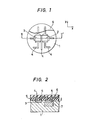
- a strain sensor is constructed by making a p-type diffused resistor 3 and an n-type diffused resistor 2 on an n-type silicon (100) substrate 1 by the use of the CMOS process.
- Fig. 1 shows a plan view
- Fig. 2 shows a sectional view taken along line II - II' in Fig. 1 and illustrates the formed states of the diffused resistors.
- the p-type diffused resistor 3 and the n-type diffused resistor 2, which is buried in a p-type diffused resistor layer 7, are respectively made in the shape of rectangles in proximity to each other, and electrode terminals 4 are provided on the four sides of each rectangle.
- the electrode terminals 4 are isolated by an SiO2film 5, and the whole surface is covered with a passivation film 6.
- the direction along the line II - II' is set to be the x-direction, and the direction orthogonal thereto in the same plane is set to be the y-direction. A method of measuring the changes of a resistivity in each diffused resistor will be described.
- four independent resistivity changes can be measured within the (100) crystal plane of silicon, and this brings forth the effect that stresses G' x and G' y in the directions of two axes, a shear stress ⁇ xy and a stress G' z perpendicular to the plane, which act on the crystal plane, can be uniquely determined.
- FIG. 3 shows a plan view of a thin-film stress/strain sensor to which the present invention is applied.
- a single-crystal thin film of silicon having the (100) plane is formed on a film substrate (of, for example, PIQ) 8, and p-type diffused resistors 3 and n-type diffused resistors 2 are formed as shown in the figure.
- the ends of these diffused resistors 2 and 3 on one side are connected by a common pattern 12, and are held in communication with a common electrode terminal 13.
- the single-crystal thin film is produced by a thin-film manufacturing process such as vacuum evaporation, CVD (Chemical Vapored Deposition), sputtering evaporation or epitaxial growth.
- a thin-film manufacturing process such as vacuum evaporation, CVD (Chemical Vapored Deposition), sputtering evaporation or epitaxial growth.
- ⁇ ij denotes a piezoresistance coefficient in the case where the direction of the ⁇ 001> crystal axis is brought into agreement with the directions of the right-angled three axes. Since the resistivity changes in the p-type diffused resistors 3 and the n-type diffused resistors 2 are independently measured, the four components of stresses ( ⁇ ' x , ⁇ ' y , ⁇ ' z , ⁇ ' xy ) are uniquely determined. From this fact, it is apparent that the thin-film stress/strain sensor for semiconductors can be constructed.
- FIG. 4 is a sectional view in the case where a semiconductor pressure sensor is constructed.
- a p-type diffused resistor 3 and an n-type diffused resistor 2 are formed to construct a gauge.
- the single-crystal substrate I is bonded to a glass substratum 10 by a low-melting glass 9.
- an n + -type diffused resistor 11 is formed in a p-type diffused layer 7, to construct a p/n-junction, whereupon the temperature of the gauge is detected.
- a temperature compensation circuit is formed, and measurements in a wide temperature range become possible.
- the silicon substrate may be in the shape of the disc, a high degree of etching technique as in the case of making a diaphragm is dispensed with, to bring forth the effect that the available percentage in production is enhanced.
- a fourth embodiment of the piezoresistive strain sensing device of the present invention will be described with reference to Figs. 5 and 6.
- This embodiment is a stress sensor which is fabricated using an n-type silicon (111) single-crystal disc 21 as a substrate
- Fig. 5 is a plan view
- Fig. 6 is a schematic sectional view taken along line VI - VI' in Fig. 5.
- Six diffused resistors 22 and 23 formed on the substrate 21 consist of three p-type diffused layers 22 and three n-type diffused layers 23, and the ends of the respective layers 22 or 23 on one side are connected by a single aluminum pattern 24 or 32. It is assumed that the individual diffused resistors 22 or 23 be formed at angular intervals of 45 °.
- the direction of the line VI - VI' agree with the direction of the ⁇ 112> crystal axis.
- the ends of the three p-type diffused resistors 22 on one side are connected to a common electrode terminal 29 through the single common Al pattern 24, whereas the ends thereof on the other side are connected to separate electrode terminals 31 through separate Al patterns 30.
- the ends of the three n-type diffused resistors23 on one side are connected to a common electrode terminal 33 through the single common Al pattern 32, whereas the ends thereof on the other side are connected to separate electrode terminals 35 through separate Al patterns 34.
- the n-type diffused resistors 23 are formed in a p-type diffused layer 25.
- the p-type diffused layer 25 is formed with an n-type diffused resistor 28, to simultaneously make a p/n - junction for temperature compensation. Now, the operation of this sensor will be described.
- the embodiment thus far described brings forth the effect that a sensor for detecting a three-dimensional stress field can be realized, and the effect that measurements at temperatures in a wide range are permitted by utilizing a p/n-junction for temperature compensation.
- the individual diffused resistors 22 or 23 are formed at the angular intervals of 45 °. This takes it into consideration that, on the (111) crystal plane, the lengthwise directions of the resistor layers are brought into agreement with the ⁇ 112> crystal axis and the ⁇ 110> crystal axis, while one resistor layer is arranged in the direction of 45 ° between them. In principle, however, the directions of the arrangement of the resistor layers may be as desired (except a case where two or more resistors become parallel among the same kind of diffused resistor layers).
- the number of the arrangement in each kind of diffused layers may well be four or more. Since the number of stress components acting independently is six, the stress components are uniquely determined when there are at least three diffused resistors in each kind of layers, namely, at least six resistors in total. In the case of forming at least four diffused resistors in the same kind of diffused layers, at least three of them may extend in crystal orientations differing from one another.
- the semiconductor single-crystal substrate may well be replaced with a single-crystal thin film produced by a thin-film manufacturing process such as vacuum evaporation, CVD, sputtering or epitaxial growth.
- a thin-film manufacturing process such as vacuum evaporation, CVD, sputtering or epitaxial growth.
Abstract
Description
- The present invention relates to a piezoresistive strain sensing device in which diffused resistors are formed in a semiconductor single-crystal substrate. More particularly, it relates to a piezoresistive strain sensing device which is well suited to sensitively and precisely detect a stress field acting on an IC chip within a semiconductor package.
- As a device wherein a mechanical stress resulting from the application of a strain is converted into an electric signal by utilizing the piezoresistance effect of a semiconductor, there has heretofore been, for example, a semiconductor strain sensor as disclosed in the official gazette of Japanese Patent Application Laid-open No. 56-140229. In this device, a bridge circuit is formed by diffused resistors on a diaphragm of silicon, and a strain is measured by detecting the fractional change in resistivity based on the deformation of the diaphragm attendant upon a surface strain. There has also been made the trial in which a diffused resistor is formed on a silicon substrate, and the substrate is buried in a-resin as sensing means, thereby to detect a two-dimensional stress field acting within a surface formed with the diffused resistor. In either case, however, the detection on a specified stress component is aimed at, and the use has been limited. A three-dimensional stress field exists in a general structure, and mechanical strain - electricity transducers including the prior- art semiconductor strain sensor have had the problem that the three-dimensional stress field cannot be separately detected.
- An object of the present invention is to provide a piezoresistive strain sensing device which sensitively and precisely detects a stress field acting in an observation surface.
- The piezoresistive strain sensing device of the present invention consists in that p-type and n-type diffused resistors are formed in a semiconductor single-crystal substrate and that one set of diffused strain gauge is constructed of resistor gauges of both the diffused layers.
- In general, the piezoresistance effect in a semiconductor such as silicon is expressed as:

- Since, in general, the tensor of the second order such as f or X is given by a six-component vector notation, the tensor % of the fourth order is expressed as a 6 x 6-element tensor. To the end of studying a three-dimensional stress field, when the directions of three right-angled axes are respectively set as x-, y- and z-directions and xx, yy, zz, yz, zx and xy are respectively rewritten as 1 - 6, Eq. (1) can be expressed as:

- When a diffused resistor is formed on any desired single-crystal substrate and the fractional change of the resistivity thereof is detected, there are, in general, 6 stress components contributive to the fractional change of the resistivity. Since, however, the fractional change of the resistivity is detected in a two-dimensional plane formed with the diffused resistor, only 3 resistance components can be independently measured on the plane. Accordingly, when one diffused resistor is used, it is impossible in principle to separately detect the stress components.
- Therefore, a diffused strain gauge for detection needs to be constructed of a plurality of independent diffused resistors. In order to detect six independent resistance components on the same plane, at least two sorts of diffused resistors must be formed. The piezoresistance coefficients which are sensitivities to a stress differ greatly, depending upon the kinds of dopants. Accordingly, diffused resistors of the p-type and n-type are formed on a semiconductor substrate having a crystal plane, all of the crystal plane indices (h, k, ℓ) of which have values different from zero, and three independent resistance components are detected in each of the regions, whereby six independent resistance components on the same plane become detectible. Thus, the three-dimensional stress field acting in the observation plane can be uniquely determined.
- Next, when the (100) plane is assumed the xy-plane and a conventional crystal axis <001> is brought into agreement with the x-axis, the piezoresistance effect which is observed within the plane is expressed as:

- Accordingly, stress components which affect the fractional changes of resistivity are four components, and the resistivity changes which are independently detectible are of three components, so that the stress field acting in the crystal plane cannot be uniquely determined. Since, however, the piezoresistance coefficients παβ differ depending upon the kinds of dopants used for diffused resistors, the resistivity changes can be independently detected in the respective diffused regions of the p-type diffused resistor and the n-type diffused resistor which are arranged in proximity to each other, and hence, the resistivity changes of six components can be independently measured in both the regions. Accordingly, p-type and n-type diffused resistors are formed in the surface layer of a semiconductor substrate having a crystal plane orientation as to which at least one of crystal plane indices (h, k, ℓ) becomes zero (however, all the indices h, k and t do not become zero simultaneously), whereby four resistor gauges capable of independent measurements can be provided, and the four stress components influential on the resistivity changes can be uniquely determined. Further, it is readily derived from Eq. (1) or Eq. (2) that the same holds within a crystal plane in which the direction of the crystal axis <100> is included.
-
- Fig. 1 is a plan view of a first embodiment of a piezoresistive strain sensing device according to the present invention;
- Fig. 2 is a sectional view taken along line II - II' in Fig. 1;
- Fig. 3 is a plan view of a second embodiment of the piezoresistive strain sensing device of the present invention;
- Fig. 4 is a sectional view of a third embodiment of the piezoresistive strain sensing device of the present invention;
- Fig. 5 is a plan view of a fourth embodiment of the piezoresistive strain sensing device of the present invention; and
- Fig. 6 is a sectional view taken along line VI - VI' in Fig. 5.
- Now, one embodiment of a piezoresistive strain sensing device according to the present invention will be described with reference to Figs. 1 and 2. In this embodiment, a strain sensor is constructed by making a p-type diffused
resistor 3 and an n-type diffusedresistor 2 on an n-type silicon (100) substrate 1 by the use of the CMOS process. Fig. 1 shows a plan view, while Fig. 2 shows a sectional view taken along line II - II' in Fig. 1 and illustrates the formed states of the diffused resistors. The p-type diffusedresistor 3 and the n-type diffusedresistor 2, which is buried in a p-type diffusedresistor layer 7, are respectively made in the shape of rectangles in proximity to each other, andelectrode terminals 4 are provided on the four sides of each rectangle. Theelectrode terminals 4 are isolated by anSiO2film 5, and the whole surface is covered with apassivation film 6. Regarding the directions of the sides of the rectangles, the direction along the line II - II' is set to be the x-direction, and the direction orthogonal thereto in the same plane is set to be the y-direction. A method of measuring the changes of a resistivity in each diffused resistor will be described. Current is caused to flow across the two electrodes opposing in the x-direction, and the potential difference across both the electrodes is measured, whereby δfxx in the equation (3) mentioned before is measured. A similar method is performed across the two electrodes opposing in the y-direction, whereby δfyy in Eq. (3) is measured. In addition, current is caused to flow across the electrodes opposing in the x-direction, and the potential difference across the electrodes opposing in the y-direction is measured, whereby δfxy in Eq. (3) is determined. Thus, the resistivity changes of the three independent components can be measured with the single diffused resistor. When δfxy is measured with either of the p-type and n-type diffused resistors, and besides, three of δfnxx, δfnyy, δfpxx and δfpyy are measured, four independent resistivity changes can be measured within the single crystal plane. - According to the present embodiment, four independent resistivity changes can be measured within the (100) crystal plane of silicon, and this brings forth the effect that stresses G'x and G'y in the directions of two axes, a shear stress τxy and a stress G'z perpendicular to the plane, which act on the crystal plane, can be uniquely determined.
- Next, a second embodiment of the piezoresistive strain sensing device of the present invention will be described with reference to Fig. 3. This figure shows a plan view of a thin-film stress/strain sensor to which the present invention is applied. A single-crystal thin film of silicon having the (100) plane is formed on a film substrate (of, for example, PIQ) 8, and p-type diffused
resistors 3 and n-type diffusedresistors 2 are formed as shown in the figure. The ends of these diffusedresistors common pattern 12, and are held in communication with acommon electrode terminal 13. The single-crystal thin film is produced by a thin-film manufacturing process such as vacuum evaporation, CVD (Chemical Vapored Deposition), sputtering evaporation or epitaxial growth. Here, when the p-type diffusedresistors 3 are arranged along the conventional crystal axis <011> and the n-type diffusedresistors 2 along <001>, the resistivity changes of the respective resistors are expressed as:
- In Eq. (4), πij denotes a piezoresistance coefficient in the case where the direction of the <001> crystal axis is brought into agreement with the directions of the right-angled three axes. Since the resistivity changes in the p-type diffused
resistors 3 and the n-type diffusedresistors 2 are independently measured, the four components of stresses (δ'x, δ'y, δ'z, δ'xy) are uniquely determined. From this fact, it is apparent that the thin-film stress/strain sensor for semiconductors can be constructed. - Next, a third embodiment of the piezoresistive strain sensing device of the present invention will be described with reference to Fig. 4. This figure is a sectional view in the case where a semiconductor pressure sensor is constructed. In the surface layer of an n-type silicon (100) single-crystal substrate 1 in the shape of a disc, a p-type diffused
resistor 3 and an n-type diffusedresistor 2 are formed to construct a gauge. The single-crystal substrate I is bonded to aglass substratum 10 by a low-melting glass 9. Further, an n+-type diffusedresistor 11 is formed in a p-type diffusedlayer 7, to construct a p/n-junction, whereupon the temperature of the gauge is detected. Thus, a temperature compensation circuit is formed, and measurements in a wide temperature range become possible. Moreover, since the silicon substrate may be in the shape of the disc, a high degree of etching technique as in the case of making a diaphragm is dispensed with, to bring forth the effect that the available percentage in production is enhanced. - According to the embodiments thus far described, since four resistivity changes within the (100) crystal plane of a semiconductor can be measured, it is possible to realize a piezoresistive strain sensing device which can uniquely determine the four stress components acting on the (100) crystal plane; stress components in the directions of right-angled three axes, two of them being contained in the plane, and a shear stress acting within the plane.
- Next, a fourth embodiment of the piezoresistive strain sensing device of the present invention will be described with reference to Figs. 5 and 6. This embodiment is a stress sensor which is fabricated using an n-type silicon (111) single-
crystal disc 21 as a substrate Fig. 5 is a plan view, while Fig. 6 is a schematic sectional view taken along line VI - VI' in Fig. 5. Six diffusedresistors substrate 21 consist of three p-type diffusedlayers 22 and three n-type diffusedlayers 23, and the ends of therespective layers single aluminum pattern resistors resistors 22 on one side are connected to acommon electrode terminal 29 through the singlecommon Al pattern 24, whereas the ends thereof on the other side are connected to separateelectrode terminals 31 throughseparate Al patterns 30. Likewise, the ends of the three n-type diffused resistors23 on one side are connected to acommon electrode terminal 33 through the singlecommon Al pattern 32, whereas the ends thereof on the other side are connected to separateelectrode terminals 35 throughseparate Al patterns 34. The n-type diffusedresistors 23 are formed in a p-type diffusedlayer 25. In addition, theAl patterns 24 etc. are isolated by an SiO2 insulator film 26, and the whole surface is covered with apassivation film 27. The p-type diffusedlayer 25 is formed with an n-type diffusedresistor 28, to simultaneously make a p/n-junction for temperature compensation. Now, the operation of this sensor will be described. - Right-angled 3 axes are given with the x-direction being the direction of the line VI - VI', the y-direction being a direction orthogonal thereto within the plane and the z-direction being a direction perpendicular to the plane, and stresses in the axial directions and shear stresses within respective planes are respectively denoted by δ' and τ. In Fig. 5, a resistivity on the line VI - VI' is denoted by δ2, that on the left side thereof is denoted by fl, and that on the right side thereof is denoted by δ3. Then, the corresponding resistivity changes are expressed as:

- As the diffused resistors of the p-type diffused
layers 22 and those of the n-type diffusedlayers 23, the values of the piezoresistance coefficients πi (i = d, P, ...) are different, so that six sorts of independent resistivity changes can be measured. Since stress components contributive to the respective resistivity changes are of six sorts, the respective components of the stress tensor or the three-dimensional stress field are/is separately detected by solving the matrix of Eq. (2). - The embodiment thus far described brings forth the effect that a sensor for detecting a three-dimensional stress field can be realized, and the effect that measurements at temperatures in a wide range are permitted by utilizing a p/n-junction for temperature compensation.
- In the foregoing embodiment, the individual diffused
resistors - Although the three diffused resistors are arranged in each kind of diffused layers, the number of the arrangement in each kind of diffused layers may well be four or more. Since the number of stress components acting independently is six, the stress components are uniquely determined when there are at least three diffused resistors in each kind of layers, namely, at least six resistors in total. In the case of forming at least four diffused resistors in the same kind of diffused layers, at least three of them may extend in crystal orientations differing from one another.
- In an actual measurement, changes in the resistivities of the diffused resistors are respectively detected.
- In each of the foregoing embodiments, the semiconductor single-crystal substrate may well be replaced with a single-crystal thin film produced by a thin-film manufacturing process such as vacuum evaporation, CVD, sputtering or epitaxial growth.
- According to each embodiment described above, six sorts of independent resistivity changes caused by the piezoresistance effect can be detected on an identical semiconductor single-crystal substrate and hence, a stress sensor for determining a three-dimensional stress field can be realized.
Claims (22)
Applications Claiming Priority (4)
| Application Number | Priority Date | Filing Date | Title |
|---|---|---|---|
| JP54473/85 | 1985-03-20 | ||
| JP5447385A JPH0697697B2 (en) | 1985-03-20 | 1985-03-20 | Semiconductor pressure converter |
| JP54474/85 | 1985-03-20 | ||
| JP5447485A JPS61214583A (en) | 1985-03-20 | 1985-03-20 | Semiconductor pressure converter |
Publications (3)
| Publication Number | Publication Date |
|---|---|
| EP0195232A2 true EP0195232A2 (en) | 1986-09-24 |
| EP0195232A3 EP0195232A3 (en) | 1989-10-25 |
| EP0195232B1 EP0195232B1 (en) | 1991-12-11 |
Family
ID=26395238
Family Applications (1)
| Application Number | Title | Priority Date | Filing Date |
|---|---|---|---|
| EP86101679A Expired EP0195232B1 (en) | 1985-03-20 | 1986-02-10 | Piezoresistive strain sensing device |
Country Status (3)
| Country | Link |
|---|---|
| US (1) | US4739381A (en) |
| EP (1) | EP0195232B1 (en) |
| DE (1) | DE3682793D1 (en) |
Cited By (9)
| Publication number | Priority date | Publication date | Assignee | Title |
|---|---|---|---|---|
| US5076106A (en) * | 1990-03-21 | 1991-12-31 | Amp Incorporated | Normal force transducer |
| US5341688A (en) * | 1991-12-26 | 1994-08-30 | Kabushiki Kaisha Toyota Chuo Kenkyusho | Force transducer |
| EP0625701A1 (en) * | 1987-04-24 | 1994-11-23 | Enplas Laboratories, Inc. | Force detector using piezoresistive elements |
| EP0729019A2 (en) * | 1995-02-27 | 1996-08-28 | Motorola, Inc. | Method of forming a piezoresistive pressure sensor and a piezoresistive pressure sensor |
| EP1496344A2 (en) * | 2003-07-09 | 2005-01-12 | Austriamicrosystems AG | Integrated semiconductive arrangement and procedure for producing a pressure dependent signal as well as a temperature dependent signal |
| EP1785710A2 (en) | 2005-11-10 | 2007-05-16 | Honeywell International Inc. | Pressure Sensor Housing and Configuration |
| EP3323778A1 (en) * | 2016-11-22 | 2018-05-23 | NXP USA, Inc. | Mems device and method for calibrating a mems device |
| CN110333221A (en) * | 2019-07-15 | 2019-10-15 | 天津大学 | { 110 } crystal face plane stress component measurement method and system |
| WO2021185003A1 (en) * | 2020-03-19 | 2021-09-23 | 深圳纽迪瑞科技开发有限公司 | Pressure-induction structure and electronic product |
Families Citing this family (13)
| Publication number | Priority date | Publication date | Assignee | Title |
|---|---|---|---|---|
| US4873871A (en) * | 1988-06-17 | 1989-10-17 | Motorola, Inc. | Mechanical field effect transistor sensor |
| US5119166A (en) * | 1990-02-06 | 1992-06-02 | Honeywell Inc. | Hall effect element aligned to reduce package-induced offsets |
| US5172205A (en) * | 1990-09-26 | 1992-12-15 | Nissan Motor Co., Ltd. | Piezoresistive semiconductor device suitable for use in a pressure sensor |
| JP3114453B2 (en) * | 1993-10-05 | 2000-12-04 | 株式会社日立製作所 | Physical quantity detection sensor and process state detector |
| JP4161410B2 (en) * | 1997-07-25 | 2008-10-08 | 株式会社デンソー | Pressure detection device |
| US6550337B1 (en) | 2000-01-19 | 2003-04-22 | Measurement Specialties, Inc. | Isolation technique for pressure sensing structure |
| US7082835B2 (en) * | 2003-06-18 | 2006-08-01 | Honeywell International Inc. | Pressure sensor apparatus and method |
| DE102004003853B4 (en) * | 2004-01-26 | 2009-12-17 | Infineon Technologies Ag | Device and method for compensation of piezo influences on an integrated circuit arrangement |
| US7921731B2 (en) * | 2007-12-03 | 2011-04-12 | The United States Of America As Represented By The Administrator Of The National Aeronautics And Space Administration | Two-axis direct fluid shear stress sensor |
| JP5686392B2 (en) * | 2010-11-24 | 2015-03-18 | ザ ガヴァナーズ オブ ザ ユニバーシティー オブ アルバータThe Governors Of The University Of Alberta | New embedded 3D stress and temperature sensor using silicon doping operation |
| JP5649478B2 (en) * | 2011-02-16 | 2015-01-07 | 三菱電機株式会社 | Semiconductor device and test method thereof |
| US10352792B2 (en) * | 2017-02-15 | 2019-07-16 | Texas Instruments Incorporated | Device and method for on-chip mechanical stress sensing |
| CN113227954A (en) * | 2018-12-20 | 2021-08-06 | 深圳纽迪瑞科技开发有限公司 | Pressure sensing device, pressure sensing method and electronic terminal |
Citations (10)
| Publication number | Priority date | Publication date | Assignee | Title |
|---|---|---|---|---|
| US3132788A (en) * | 1961-10-25 | 1964-05-12 | Axel H Johnson | Tape transporting means for a magnetic recorder |
| US3277698A (en) * | 1963-11-15 | 1966-10-11 | Bell Telephone Labor Inc | Stress sensing semiconductive devices |
| US3491274A (en) * | 1965-06-04 | 1970-01-20 | Centre Electron Horloger | Diffused resistance in an integrated circuit |
| US3537319A (en) * | 1968-07-26 | 1970-11-03 | Gen Electric | Silicon diaphragm with optimized integral strain gages |
| US3899695A (en) * | 1973-09-24 | 1975-08-12 | Nat Semiconductor Corp | Semiconductor pressure transducer employing novel temperature compensation means |
| JPS5660066A (en) * | 1979-10-19 | 1981-05-23 | Nec Corp | Semiconductor strain detector |
| WO1981003086A1 (en) * | 1980-04-14 | 1981-10-29 | Motorola Inc | Silicon pressure sensor |
| JPS56140229A (en) * | 1980-04-02 | 1981-11-02 | Toshiba Corp | Pressure converter |
| JPS5795673A (en) * | 1980-12-05 | 1982-06-14 | Toshiba Corp | Pressure sensitive semiconductor device |
| EP0146709B1 (en) * | 1983-12-16 | 1990-07-18 | Hitachi, Ltd. | Pressure sensor |
Family Cites Families (6)
| Publication number | Priority date | Publication date | Assignee | Title |
|---|---|---|---|---|
| US3123788A (en) * | 1964-03-03 | Piezoresistive gage | ||
| FR1522471A (en) * | 1967-03-15 | 1968-04-26 | Csf | Stress measuring device |
| US4028564A (en) * | 1971-09-22 | 1977-06-07 | Robert Bosch G.M.B.H. | Compensated monolithic integrated current source |
| US3818289A (en) * | 1972-04-10 | 1974-06-18 | Raytheon Co | Semiconductor integrated circuit structures |
| US3922705A (en) * | 1973-06-04 | 1975-11-25 | Gen Electric | Dielectrically isolated integral silicon diaphram or other semiconductor product |
| US4510671A (en) * | 1981-08-31 | 1985-04-16 | Kulite Semiconductor Products, Inc. | Dielectrically isolated transducer employing single crystal strain gages |
-
1986
- 1986-02-10 EP EP86101679A patent/EP0195232B1/en not_active Expired
- 1986-02-10 DE DE8686101679T patent/DE3682793D1/en not_active Expired - Lifetime
- 1986-03-12 US US06/838,954 patent/US4739381A/en not_active Expired - Lifetime
Patent Citations (10)
| Publication number | Priority date | Publication date | Assignee | Title |
|---|---|---|---|---|
| US3132788A (en) * | 1961-10-25 | 1964-05-12 | Axel H Johnson | Tape transporting means for a magnetic recorder |
| US3277698A (en) * | 1963-11-15 | 1966-10-11 | Bell Telephone Labor Inc | Stress sensing semiconductive devices |
| US3491274A (en) * | 1965-06-04 | 1970-01-20 | Centre Electron Horloger | Diffused resistance in an integrated circuit |
| US3537319A (en) * | 1968-07-26 | 1970-11-03 | Gen Electric | Silicon diaphragm with optimized integral strain gages |
| US3899695A (en) * | 1973-09-24 | 1975-08-12 | Nat Semiconductor Corp | Semiconductor pressure transducer employing novel temperature compensation means |
| JPS5660066A (en) * | 1979-10-19 | 1981-05-23 | Nec Corp | Semiconductor strain detector |
| JPS56140229A (en) * | 1980-04-02 | 1981-11-02 | Toshiba Corp | Pressure converter |
| WO1981003086A1 (en) * | 1980-04-14 | 1981-10-29 | Motorola Inc | Silicon pressure sensor |
| JPS5795673A (en) * | 1980-12-05 | 1982-06-14 | Toshiba Corp | Pressure sensitive semiconductor device |
| EP0146709B1 (en) * | 1983-12-16 | 1990-07-18 | Hitachi, Ltd. | Pressure sensor |
Non-Patent Citations (4)
| Title |
|---|
| PATENT ABSTRACTS OF JAPAN vol. 5, no. 121 (E-68)(793) 5 August 1981; & JP-A-56 060 066 (NIPPON DENKI K.K.) 23.05.1981 * |
| PATENT ABSTRACTS OF JAPAN vol. 6, no. 18 (P-100)(896) 2 February 1982; & JP-A-56 140 229 (TOKYO SHIBAURA DENKI K.K.) 02.11.1981 * |
| PATENT ABSTRACTS OF JAPAN vol. 6, no. 182 (E-131)(1060) 18 September 1982; & JP-A-57 095 673 (TOKYO SHIBAURA DENKI K.K.) 14.06.1982 * |
| PHYSICAL REVIEW vol. 94, no. 1, 1 April 1954, pages 42-49; C.S. SMITH: "Piezoresistance Effect in Germanium and Silicon" * |
Cited By (14)
| Publication number | Priority date | Publication date | Assignee | Title |
|---|---|---|---|---|
| EP0625701A1 (en) * | 1987-04-24 | 1994-11-23 | Enplas Laboratories, Inc. | Force detector using piezoresistive elements |
| US5076106A (en) * | 1990-03-21 | 1991-12-31 | Amp Incorporated | Normal force transducer |
| US5341688A (en) * | 1991-12-26 | 1994-08-30 | Kabushiki Kaisha Toyota Chuo Kenkyusho | Force transducer |
| EP0729019A2 (en) * | 1995-02-27 | 1996-08-28 | Motorola, Inc. | Method of forming a piezoresistive pressure sensor and a piezoresistive pressure sensor |
| EP0729019A3 (en) * | 1995-02-27 | 1996-12-11 | Motorola Inc | Method of forming a piezoresistive pressure sensor and a piezoresistive pressure sensor |
| DE10331096B4 (en) * | 2003-07-09 | 2014-02-13 | Austriamicrosystems Ag | Integrated semiconductor device and method |
| EP1496344A3 (en) * | 2003-07-09 | 2008-02-06 | Austriamicrosystems AG | Integrated semiconductive arrangement and procedure for producing a pressure dependent signal as well as a temperature dependent signal |
| EP1496344A2 (en) * | 2003-07-09 | 2005-01-12 | Austriamicrosystems AG | Integrated semiconductive arrangement and procedure for producing a pressure dependent signal as well as a temperature dependent signal |
| EP1785710A2 (en) | 2005-11-10 | 2007-05-16 | Honeywell International Inc. | Pressure Sensor Housing and Configuration |
| EP1785710A3 (en) * | 2005-11-10 | 2008-06-25 | Honeywell International Inc. | Pressure Sensor Housing and Configuration |
| EP3323778A1 (en) * | 2016-11-22 | 2018-05-23 | NXP USA, Inc. | Mems device and method for calibrating a mems device |
| US10683202B2 (en) | 2016-11-22 | 2020-06-16 | Nxp Usa, Inc. | MEMS device and method for calibrating a MEMS device |
| CN110333221A (en) * | 2019-07-15 | 2019-10-15 | 天津大学 | { 110 } crystal face plane stress component measurement method and system |
| WO2021185003A1 (en) * | 2020-03-19 | 2021-09-23 | 深圳纽迪瑞科技开发有限公司 | Pressure-induction structure and electronic product |
Also Published As
| Publication number | Publication date |
|---|---|
| EP0195232B1 (en) | 1991-12-11 |
| US4739381A (en) | 1988-04-19 |
| DE3682793D1 (en) | 1992-01-23 |
| EP0195232A3 (en) | 1989-10-25 |
Similar Documents
| Publication | Publication Date | Title |
|---|---|---|
| EP0195232B1 (en) | Piezoresistive strain sensing device | |
| US10775248B2 (en) | MEMS strain gauge sensor and manufacturing method | |
| EP0311695B1 (en) | Force and moment detector using resistor | |
| US5485753A (en) | Piezoresistive silicon pressure sensor implementing long diaphragms with large aspect ratios | |
| US4430895A (en) | Piezoresistive accelerometer | |
| EP0735352B1 (en) | Force transducer and method of fabrication thereof | |
| US6973836B2 (en) | Semiconductor pressure sensor having diaphragm | |
| KR840002283B1 (en) | Silicon pressure sensor | |
| KR930003148B1 (en) | Pressure sensor | |
| US5239870A (en) | Semiconductor acceleration sensor with reduced cross axial sensitivity | |
| JPH0479420B2 (en) | ||
| US10910500B2 (en) | Load sensing devices, packages, and systems | |
| JPH0833409B2 (en) | Acceleration measuring device and manufacturing method thereof | |
| US20190074231A1 (en) | Stress Sensor for Semiconductor Components | |
| US4565097A (en) | Method and apparatus for transducer error cancellation | |
| EP0456190B1 (en) | Piezoresistive accelerometer | |
| US3329023A (en) | Semiconductor strain gage transducers | |
| US6763719B2 (en) | Acceleration sensor | |
| US7536919B2 (en) | Strain gauge | |
| US4422063A (en) | Semiconductor strain gauge | |
| CN111498795B (en) | Pressure sensor chip with isolation groove array structure and preparation method thereof | |
| US20050268726A1 (en) | Thick film strain gage sensor | |
| JPH0697697B2 (en) | Semiconductor pressure converter | |
| RU2050033C1 (en) | Integral tension transducer | |
| CN116678544B (en) | Silicon strain gauge and manufacturing method thereof |
Legal Events
| Date | Code | Title | Description |
|---|---|---|---|
| PUAI | Public reference made under article 153(3) epc to a published international application that has entered the european phase |
Free format text: ORIGINAL CODE: 0009012 |
|
| AK | Designated contracting states |
Kind code of ref document: A2 Designated state(s): DE FR GB |
|
| PUAL | Search report despatched |
Free format text: ORIGINAL CODE: 0009013 |
|
| AK | Designated contracting states |
Kind code of ref document: A3 Designated state(s): DE FR GB |
|
| 17P | Request for examination filed |
Effective date: 19890912 |
|
| 17Q | First examination report despatched |
Effective date: 19900723 |
|
| GRAA | (expected) grant |
Free format text: ORIGINAL CODE: 0009210 |
|
| AK | Designated contracting states |
Kind code of ref document: B1 Designated state(s): DE FR GB |
|
| REF | Corresponds to: |
Ref document number: 3682793 Country of ref document: DE Date of ref document: 19920123 |
|
| ET | Fr: translation filed | ||
| PLBE | No opposition filed within time limit |
Free format text: ORIGINAL CODE: 0009261 |
|
| STAA | Information on the status of an ep patent application or granted ep patent |
Free format text: STATUS: NO OPPOSITION FILED WITHIN TIME LIMIT |
|
| 26N | No opposition filed | ||
| REG | Reference to a national code |
Ref country code: GB Ref legal event code: IF02 |
|
| PGFP | Annual fee paid to national office [announced via postgrant information from national office to epo] |
Ref country code: FR Payment date: 20040122 Year of fee payment: 19 |
|
| PGFP | Annual fee paid to national office [announced via postgrant information from national office to epo] |
Ref country code: GB Payment date: 20040202 Year of fee payment: 19 |
|
| PGFP | Annual fee paid to national office [announced via postgrant information from national office to epo] |
Ref country code: DE Payment date: 20040304 Year of fee payment: 19 |
|
| PG25 | Lapsed in a contracting state [announced via postgrant information from national office to epo] |
Ref country code: GB Free format text: LAPSE BECAUSE OF NON-PAYMENT OF DUE FEES Effective date: 20050210 |
|
| PG25 | Lapsed in a contracting state [announced via postgrant information from national office to epo] |
Ref country code: DE Free format text: LAPSE BECAUSE OF NON-PAYMENT OF DUE FEES Effective date: 20050901 |
|
| GBPC | Gb: european patent ceased through non-payment of renewal fee |
Effective date: 20050206 |
|
| PG25 | Lapsed in a contracting state [announced via postgrant information from national office to epo] |
Ref country code: FR Free format text: LAPSE BECAUSE OF NON-PAYMENT OF DUE FEES Effective date: 20051031 |
|
| REG | Reference to a national code |
Ref country code: FR Ref legal event code: ST Effective date: 20051031 |