EP0193462B1 - High frequency pin-type diode with abrupt junctions - Google Patents
High frequency pin-type diode with abrupt junctions Download PDFInfo
- Publication number
- EP0193462B1 EP0193462B1 EP19860400379 EP86400379A EP0193462B1 EP 0193462 B1 EP0193462 B1 EP 0193462B1 EP 19860400379 EP19860400379 EP 19860400379 EP 86400379 A EP86400379 A EP 86400379A EP 0193462 B1 EP0193462 B1 EP 0193462B1
- Authority
- EP
- European Patent Office
- Prior art keywords
- diode
- layers
- layer
- zone
- pin
- Prior art date
- Legal status (The legal status is an assumption and is not a legal conclusion. Google has not performed a legal analysis and makes no representation as to the accuracy of the status listed.)
- Expired
Links
- 239000000758 substrate Substances 0.000 claims description 16
- 230000007704 transition Effects 0.000 claims description 15
- 229910052698 phosphorus Inorganic materials 0.000 claims description 11
- 239000012535 impurity Substances 0.000 claims description 6
- XUIMIQQOPSSXEZ-UHFFFAOYSA-N Silicon Chemical compound [Si] XUIMIQQOPSSXEZ-UHFFFAOYSA-N 0.000 claims description 5
- 229910052710 silicon Inorganic materials 0.000 claims description 5
- 239000010703 silicon Substances 0.000 claims description 5
- 238000009792 diffusion process Methods 0.000 description 7
- 238000000407 epitaxy Methods 0.000 description 7
- 230000007423 decrease Effects 0.000 description 6
- 238000010586 diagram Methods 0.000 description 4
- 230000015556 catabolic process Effects 0.000 description 3
- 239000002800 charge carrier Substances 0.000 description 3
- 238000005553 drilling Methods 0.000 description 3
- 239000000463 material Substances 0.000 description 3
- 238000000034 method Methods 0.000 description 3
- 239000000969 carrier Substances 0.000 description 2
- 238000001465 metallisation Methods 0.000 description 2
- ZOXJGFHDIHLPTG-UHFFFAOYSA-N Boron Chemical compound [B] ZOXJGFHDIHLPTG-UHFFFAOYSA-N 0.000 description 1
- OAICVXFJPJFONN-UHFFFAOYSA-N Phosphorus Chemical compound [P] OAICVXFJPJFONN-UHFFFAOYSA-N 0.000 description 1
- 229910018885 Pt—Au Inorganic materials 0.000 description 1
- 230000005540 biological transmission Effects 0.000 description 1
- 229910052796 boron Inorganic materials 0.000 description 1
- 238000005520 cutting process Methods 0.000 description 1
- 229940082150 encore Drugs 0.000 description 1
- 238000009776 industrial production Methods 0.000 description 1
- 238000004519 manufacturing process Methods 0.000 description 1
- 230000000873 masking effect Effects 0.000 description 1
- 230000003071 parasitic effect Effects 0.000 description 1
- 239000011574 phosphorus Substances 0.000 description 1
- 239000004065 semiconductor Substances 0.000 description 1
- 239000007858 starting material Substances 0.000 description 1
Images

Classifications
-
- H—ELECTRICITY
- H01—ELECTRIC ELEMENTS
- H01L—SEMICONDUCTOR DEVICES NOT COVERED BY CLASS H10
- H01L29/00—Semiconductor devices adapted for rectifying, amplifying, oscillating or switching, or capacitors or resistors with at least one potential-jump barrier or surface barrier, e.g. PN junction depletion layer or carrier concentration layer; Details of semiconductor bodies or of electrodes thereof ; Multistep manufacturing processes therefor
- H01L29/66—Types of semiconductor device ; Multistep manufacturing processes therefor
- H01L29/86—Types of semiconductor device ; Multistep manufacturing processes therefor controllable only by variation of the electric current supplied, or only the electric potential applied, to one or more of the electrodes carrying the current to be rectified, amplified, oscillated or switched
- H01L29/861—Diodes
- H01L29/868—PIN diodes
Definitions
- the present invention relates to the field of semiconductors, and more specifically a PIN type microwave diode, on silicon, with low series resistance, produced by epitaxy of lightly doped layers, of P and N conductivity types, on an intrinsic or high substrate. resistivity.
- PIN diodes are well known and they are normally obtained by scattering in a high resistivity substrate: P-type scattering on one side of the substrate wafer, and N-type scattering on the other side of this wafer.
- the drawback is that, as a consequence of the diffusion process, the doping rate of the P and N layers is very high at the surface of the wafer and very low at the interface between the doped layer and the undoped substrate.
- PI and IN which are not abrupt: this obliges to apply a reverse bias voltage high to reduce the losses in the layers P and N, but it is then necessary to increase the thickness of the substrate I so that the diode is not destroyed by breakdown when the voltage of the microwave signal is added to the reverse bias voltage.
- the increase in the thickness of the substrate 1 causes the resistance in the forward direction of the diode to increase.
- the invention proposes a PIN diode, whose transitions PI and 1-N, between P and intrinsic layers on the one hand and between intrinsic and N layers on the other hand, are steep, and whose substrate, that is to say -to say the intrinsic layer has a high resistivity, which is equivalent to a low direct series resistance.
- the abrupt transitions are obtained by means of two layers P and N - one on each face of the substrate - which are epitaxial, instead of being diffused according to the prior art.
- these two layers are from 10 to 100 times less doped than the diffused or epitaxial layers of the prior art: their doping level is of the order of approximately 101 7 to 1018, compared to a doping level of 1 'order from 1019 to 1020 in diffused or epitaxial diodes according to known art.
- the doping level being constant throughout the thickness of the epitaxial layers - except in two overdoped wells for metallization with low contact resistance - the junctions are steep.
- the invention relates to a PIN type microwave diode according to claim 1.
- Figure 1 shows a sectional view of a PIN diode according to the prior art. Very simple in structure, it is obtained from a wafer of material - generally silicon - of high resistivity p, around 4000 ⁇ / cm, of type P not compensated which is called 1 (intrinsic) or 7 t, that is to say P involuntarily doped: the level of doping is indeed very low, of the order of 2.10 12 at.cm- 3 . It is the material of this wafer which provides the layer 1 marked 1.
- P-type impurities for example boron
- N-type impurities for example phosphorus
- Two metallizations - not shown - deposited on the external faces of layers 2 and 3 ensure an ohmic contact making contact of very low resistance. They are produced according to a known process such as Ni-Au or by the "chain" SiPt-Ti-Pt-Au.
- the level of doping in the thickness of layers 2 and 3 changes, for example, from 1020 or 10 1 9 to around 2.1012 at the PI junction and at the IN junction: this is represented by curve 5 for layer 2, and by curve 6 for layer 3.
- transistions P-I and I-N are not abrupt but gradual, and this occurs on the resistances of layers 2 and 3, which vary with the voltage to which they are subjected.
- the reverse bias voltage -V is greater than the piercing voltage -Vp.
- Vp being the voltage for which zone I of the diode is in charge of space, that is to say does not contain any more carriers of free charges (electrons and holes), but only fixed charges which are due to atoms ionized impurities (negatively for the P- or ⁇ type).
- the second case of the operating range of a PIN diode is that where the reverse voltage is lower than the piercing voltage -Vp.
- the resistances Rp and R N of the layers P and N, 2 and 3 respectively, are at or near their maximum values, since, according to FIG. 3, the resistance increases when the voltage decreases.
- the sum of the lengths W 1 and W 2 of the two zones is equal to the length W of the zone I.
- the loss introduced in reverse voltage is lower as p is higher in pW 2 / S.
- the PIN diode according to the invention is produced - collectively of course - from a perfectly ground silicon wafer and therefore of well controlled thickness, which corresponds to zone I marked 8.
- This wafer is not intentionally doped, that is to say that its level of impurities is around 1012.
- the doping levels, during the epitaxies are 10 to 100 times less than the usual doping levels: they are at the level of 5.1016 to 5.1018 at.cm -3, while we know of epitaxial diodes but at levels higher than 1019 at.cm -3 , which introduces mechanical stresses between highly doped layers and zone I, and therefore decreases the lifetime ⁇ , like this has been said.
- the substrate 8 which now constitutes the zone I, of well defined length W, is undoped, at a level of 2.1012 for example, represented by the line 13.
- the doping level of the layers P 9 and N 10 is represented by the horizontal lines 14 and 15, around 5.1016-5.1018. Since the doping rate was kept constant throughout the duration of the epitaxies - except the final overdoping for the contacts - and there is no diffusion of impurities in the substrate, or zone I, the PI transitions and I ⁇ N are steep and represented by lines 16 and 17 respectively, almost vertical on this graph.
- the PIN diode according to the invention has much less mechanical stress than the diodes according to the known art, since the P and N layers are less doped: consequently, the lifetime ⁇ of the charge carriers is higher, which decreases direct resistance R D.
- the PIN diode according to the invention is of general use, but it is especially used in microwave.
Description
La présente invention concerne le domaine des semiconducteurs, et plus précisément une diode hyperfréquence de type PIN, sur silicium, à faible résistance série, réalisée par épitaxie de couches peu dopées, de types de conductivité P et N, sur un substrat intrinsèque ou de haute résistivité.The present invention relates to the field of semiconductors, and more specifically a PIN type microwave diode, on silicon, with low series resistance, produced by epitaxy of lightly doped layers, of P and N conductivity types, on an intrinsic or high substrate. resistivity.
Les diodes PIN sont bien connues et elles sont normalement obtenues par diffusions dans un substrat de haute résistivité: une diffusion de type P sur une face de la tranche de substrat, et une diffusion de type N sur l'autre face de cette tranche. L'inconvénient est que, comme conséquence du procédé de diffusion, le taux de dopage des couches P et N est très élevé en surface de la tranche et très faible à l'interface entre couche dopée et substrat non dopé. Il y a donc deux transistions, P-I et I-N, qui ne sont pas abruptes: ceci oblige à appliquer une tension inverse de polarisation élevée pour réduire les pertes dans les couches P et N, mais il est alors nécessaire d'augmenter l'épaisseur du substrat I pour que la diode ne soit pas détruite par claquage lorsqu'à la tension inverse de polarisation est ajoutée la tension du signal hyperfréquence. Or l'augmentation de l'épaisseur du substrat 1 entraine l'augmentation de la résistance en sens direct de la diode.PIN diodes are well known and they are normally obtained by scattering in a high resistivity substrate: P-type scattering on one side of the substrate wafer, and N-type scattering on the other side of this wafer. The drawback is that, as a consequence of the diffusion process, the doping rate of the P and N layers is very high at the surface of the wafer and very low at the interface between the doped layer and the undoped substrate. There are therefore two transistions, PI and IN, which are not abrupt: this obliges to apply a reverse bias voltage high to reduce the losses in the layers P and N, but it is then necessary to increase the thickness of the substrate I so that the diode is not destroyed by breakdown when the voltage of the microwave signal is added to the reverse bias voltage. However, the increase in the thickness of the substrate 1 causes the resistance in the forward direction of the diode to increase.
L'invention propose une diode PIN, dont les transitions P-I et 1-N, entre couches P et intrinsèque d'une part et entre couches intrinsèque et N d'autre part, sont abruptes, et dont le substrat, c'est-à-dire la couche intrinsèque a une résistivité élevée, ce qui équivaut à une faible résistance série en direct. Les transitions abruptes sont obtenues au moyen de deux couches P et N - une sur chaque face du substrat - qui sont épitaxiées, au lieu d'être diffusées selon l'art antérieur. De plus, ces deux couches sont de 10 à 100 fois moins dopées que les couches diffusées ou épitaxiées de l'art antérieur: leur niveau de dopage est de l'ordre de 1017 environ à 1018, comparé à un niveau de dopage de l'ordre de 1019 à 1020 dans les diodes diffusées ou épitaxiées suivant l'art connu. Le niveau de dopage étant constant dans toute l'épaisseur des couches épitaxiées - sauf en deux caissons surdopés pour métallisation à faible résistance de contact - les jonctions sont abruptes.The invention proposes a PIN diode, whose transitions PI and 1-N, between P and intrinsic layers on the one hand and between intrinsic and N layers on the other hand, are steep, and whose substrate, that is to say -to say the intrinsic layer has a high resistivity, which is equivalent to a low direct series resistance. The abrupt transitions are obtained by means of two layers P and N - one on each face of the substrate - which are epitaxial, instead of being diffused according to the prior art. In addition, these two layers are from 10 to 100 times less doped than the diffused or epitaxial layers of the prior art: their doping level is of the order of approximately 101 7 to 1018, compared to a doping level of 1 'order from 1019 to 1020 in diffused or epitaxial diodes according to known art. The doping level being constant throughout the thickness of the epitaxial layers - except in two overdoped wells for metallization with low contact resistance - the junctions are steep.
De façon plus précise, l'invention concerne une diode hyperfréquence de type PIN selon la revendication 1.More specifically, the invention relates to a PIN type microwave diode according to claim 1.
L'invention sera mieux comprise par la description qui suit d'un exemple de réalisation de diode PIN et des explications de son fonctionnement, ainsi que de son procédé de fabrication, cette description s'appuyant sur les figures jointes en annexes, qui représentent:
- - figure 1: vue en coupe d'une diode PIN selon l'art connu, superposée au profil de dopage de cette diode,
- - figure 2: schéma équivalent d'une diode PIN soumise à une tension inverse de polarisation supérieure à la tension de perçage,
- - figure 3: courbe des capacités et résistances d'une diode PIN, en fonction de la tension,
- - figure 4: schéma équivalent d'une diode PIN soumise à une tension inverse de polarisation inférieure à la tension de perçage,
- - figure 5: vue en coupe d'une diode PIN selon l'invention superposée à son profil de dopage.
- FIG. 1: sectional view of a PIN diode according to known art, superimposed on the doping profile of this diode,
- - Figure 2: equivalent diagram of a PIN diode subjected to a reverse bias voltage greater than the piercing voltage,
- FIG. 3: curve of the capacities and resistances of a PIN diode, as a function of the voltage,
- - Figure 4: equivalent diagram of a PIN diode subjected to a reverse bias voltage lower than the piercing voltage,
- - Figure 5: sectional view of a PIN diode according to the invention superimposed on its doping profile.
La simplicité de l'invention, et les caractéristiques de la diode PIN qui en résulte, seront mieux comprises par un exposé préalable des conditions de fonctionnement d'une diode PIN, et par comparaison avec une diode PIN selon l'art antérieur.The simplicity of the invention, and the characteristics of the resulting PIN diode, will be better understood by a prior description of the operating conditions of a PIN diode, and by comparison with a PIN diode according to the prior art.
La figure 1 représente une vue en coupe d'une diode PIN selon l'art connu. De structure très simple, elle est obtenue à partir d'une tranche de matériau - généralement du silicium - de haute résistivité p, environ 4000 Ω/cm, de type P non compensé que l'on dénomme 1 (intrinsèque) ou 7t, c'est-à-dire P involontairement dopé: le niveau de dopage est en effet très faible, de l'ordre de 2.1012 at.cm-3. C'est le matériau de cette tranche qui fournit la couche 1 repérée 1.Figure 1 shows a sectional view of a PIN diode according to the prior art. Very simple in structure, it is obtained from a wafer of material - generally silicon - of high resistivity p, around 4000 Ω / cm, of type P not compensated which is called 1 (intrinsic) or 7 t, that is to say P involuntarily doped: the level of doping is indeed very low, of the order of 2.10 12 at.cm- 3 . It is the material of this wafer which provides the layer 1 marked 1.
Par deux diffusions successives, et en prenant bien entendu les mesures de masquages appropriées, on diffuse des impuretés de type P, par exemple du bore, sur une face de la tranche pour créer une couche P repérée 2, puis des impuretés de type N, par exemple du phosphore, sur l'autre face de la tranche, pour créer une couche N repérée 3. Les deux diffusions sont en général menées à la même profondeur, de l'ordre de 20 µm par exemple.By two successive diffusions, and of course by taking the appropriate masking measures, P-type impurities, for example boron, are diffused on one face of the wafer to create a layer P marked 2, then N-type impurities, for example phosphorus, on the other face of the wafer, to create a layer N marked 3. The two diffusions are generally carried out at the same depth, of the order of 20 μm for example.
Deux métallisations - non représentées - déposées sur les faces externes des couches 2 et 3 assurent un contact ohmique de prise de contact de très faible résistance. Elles sont réalisées selon un procédé connu tel que Ni-Au ou par la "chaine" SiPt-Ti-Pt-Au.Two metallizations - not shown - deposited on the external faces of
Sur cette vue en coupe d'une diode PIN selon l'art connu a été superposé le profil de dopage des couches, dont le niveau "n" est porté en ordonnées. Les opérations de diffusion apportent un taux de dopage - P ou N selon la couche considérée - qui est de l'ordre de 1019 à 1020 en surface, c'est-à-dire sur les faces externes des couches 2 et 3. Or, c'est une conséquence de la diffusion que ces niveaux de dopage ne sont pas constants sur toute l'épaisseur de la couche diffusée, puisqu'il y a un front de dopage qui s'appauvrit au fur et à mesure qu'il pénètre dans la tranche initialement non dopée. Il en résulte que, si le substrat ou couche intrinsèque 1 est à l'origine, par exemple, au niveau 2.1012, le niveau de dopage dans l'épaisseur des couches 2 et 3 évolue, par exemple, de 1020 ou 1019 à environ 2.1012 à la jonction P-I et à la jonction I-N: c'est ce qui est représenté par la courbe 5 pour la couche 2, et par la courbe 6 pour la couche 3.On this sectional view of a PIN diode according to the prior art, the doping profile of the layers, the level "n" of which is plotted on the ordinate, has been superimposed. Diffusion operations provide a doping rate - P or N depending on the layer considered - which is of the order of 10 19 to 10 2 0 at the surface, that is to say on the external faces of
On dit alors que les transistions P-I et I-N ne sont pas abruptes mais graduelles, et cela intervient sur les résistances des couches 2 et 3, qui varient avec la tension à laquelle elles sont soumises.We then say that the transistions P-I and I-N are not abrupt but gradual, and this occurs on the resistances of
C'est donc un objet de la présente invention que de réaliser une diode PIN à transitions abruptes.It is therefore an object of the present invention to produce a PIN diode with abrupt transitions.
Il faut considérer trois domaines de tension pour une diode PIN.There are three voltage ranges to consider for a PIN diode.
Dans le premier cas, la tension inverse de polarisation -V est supérieure à la tension de perçage -Vp. -V >-VpIn the first case, the reverse bias voltage -V is greater than the piercing voltage -Vp. -V> -Vp
Vp étant la tension pour laquelle la zone I de la diode est en charge d'espace, c'est-à-dire ne contient plus de porteurs de charges libres (électrons et trous), mais uniquement des charges fixes qui sont dues aux atomes d'impuretés ionisées (négativement pour le type P- ou π).Vp being the voltage for which zone I of the diode is in charge of space, that is to say does not contain any more carriers of free charges (electrons and holes), but only fixed charges which are due to atoms ionized impurities (negatively for the P- or π type).
La tension de perçage est donnée en première approximation par l'expression:
- W = épaisseur de la zone I, en microns
- po = résistivité du matériau de départ, par exemple 4000Ω/c m dans l'exemple cité et pour la formule employée,
- préel: résistivité réelle de la zone 1 de la diode PIN réalisée.
- W = thickness of zone I, in microns
- p o = resistivity of the starting material, for example 4000Ω / cm in the example cited and for the formula used,
- preel: real resistivity of zone 1 of the PIN diode produced.
Comme on cherche une tension de perçage Vp la plus faible possible, pour avoir une capacité la plus faible possible de la zone I, il est nécessaire de réaliser la diode selon un processus qui conserve à p sa valeur initale (préel = po) ou, mieux, qui l'augmente.As we are looking for the lowest possible piercing voltage Vp, to have the lowest possible capacitance in zone I, it is necessary to make the diode according to a process which retains at p its initial value (preel = po) or, better, which increases it.
En charge d'espace, le schéma équivalent d'une diode PIN est donné par la figure 2, dans laquelle:
- - Rp (V) représente la résistance de la couche P pour un potentiel V
- - RN (V) représente la résistance de la couche N pour un potentiel V,
- - C représente la capacité de la zone I. C'est bien une capacité puisqu'elle est, dans ce cas, dépourvue d'électrons et de trous, et sa valeur est, comme cela est connu, donnée par l'expression

- avec ε = constante diélectrique du matériau I
- S = section offerte au passage du courant par la diode PIN
- W = longueur, ou épaisseur de la zone I.
- - Rp (V) represents the resistance of layer P for a potential V
- - R N (V) represents the resistance of the N layer for a potential V,
- - C represents the capacity of zone I. It is indeed a capacity since it is, in this case, devoid of electrons and holes, and its value is, as is known, given by the expression
- with ε = dielectric constant of the material I
- S = section offered for current flow by the PIN diode
- W = length, or thickness of zone I.
Mais, comme le montre la figure 3 qui donne les courbes de capacité et de résistance d'une diode PIN en fonction de la tension inverse, les résistances Rp et RN diminuent lorsque la tension V augmente. Simultanément, la capacité décroit dans une fraction 7 de la courbe, qui correspond aux basses fréquences, jusqu'à la valeur de la tension de perçage Vp, puis diminue beaucoup plus lentement avec la tension et cela d'autant plus lentement que les transitions sont moins graduelles.However, as shown in FIG. 3 which gives the capacitance and resistance curves of a PIN diode as a function of the reverse voltage, the resistances Rp and R N decrease when the voltage V increases. Simultaneously, the capacity decreases in a fraction 7 of the curve, which corresponds to the low frequencies, up to the value of the piercing voltage Vp, then decreases much more slowly with the voltage and this all the more slowly as the transitions are less gradual.
Plus les diffusions des couches 2 et 3 d'une diode PIN sont profondes, plus les résistances Rp et RN sont élevées, pour une tension donnée, car la résistance des transitions P-I et I-N dans la partie qui n'est pas en charge d'espace peut être importante. Si la diode est placée en shunt dans une ligne de transmission, elle amène une perte proportionnelle à (Rp + RN)C2 de sorte que des transitions pas assez abruptes obligent à appliquer une tension de polarisation élevée afin de réduire les pertes, en réduisant Rp, RN et C.The deeper the diffusions of
Mais ceci est un inconvénient, car la tension de claquage Vc d'une diode doit toujours être supérieure à la somme de la tension inverse de polarisation et de la tension de crête du signal hyperfréquence. Or, la tension de claquage Vc est liée à l'épaisseur W de la zone I par l'expression approximative: Vc = (10 à 15)WmicromètresHowever, this is a drawback, since the breakdown voltage Vc of a diode must always be greater than the sum of the reverse bias voltage and the peak voltage of the microwave signal. However, the breakdown voltage Vc is linked to the thickness W of the zone I by the approximate expression: Vc = (10 to 15) Wmicrometers
Si on augmente W pour augmenter Vc, on augmente simultanément la tension de perçage Vp, mais surtout la résistance de la diode en sens direct, ce qui est un inconvénient majeur.If we increase W to increase Vc, we simultaneously increase the piercing voltage Vp, but especially the resistance of the diode in the forward direction, which is a major drawback.
Le second cas de domaine de fonctionnement d'une diode PIN est celui où la tension inverse est inférieure à la tension de perçage -Vp.The second case of the operating range of a PIN diode is that where the reverse voltage is lower than the piercing voltage -Vp.
Le schéma équivalent de la diode est alors donné par la figure 4.The equivalent diagram of the diode is then given in FIG. 4.
Les résistances Rp et RN des couches P et N, 2 et 3 respectivement, sont à leurs valeurs maximales ou en sont proches, puisque, selon la figure 3, la résistance augmente lorsque la tension diminue.The resistances Rp and R N of the layers P and N, 2 and 3 respectively, are at or near their maximum values, since, according to FIG. 3, the resistance increases when the voltage decreases.
La zone 1 est constituée par une première zone en charge d'espace équivalente à une capacité Ci = eS/Wi, dont W1 est la longueur de cette zone, et par une deuxième zone qui n'est pas en charge d'espace, équivalente à une capacité C2 = eS/W2, shuntée par une résistance de valeur pW2/S. Bien entendu, la somme des longueurs W1 et W2 des deux zones est égale à la longueur W de la zone I.Zone 1 is constituted by a first zone in charge of space equivalent to a capacity Ci = eS / Wi, of which W 1 is the length of this zone, and by a second zone which is not in charge of space, equivalent to a capacitance C 2 = eS / W 2 , shunted by a resistor of value pW 2 / S. Of course, the sum of the lengths W 1 and W 2 of the two zones is equal to the length W of the zone I.
La perte introduite en tension inverse est d'autant plus faible que p est élevé dans pW2/S.The loss introduced in reverse voltage is lower as p is higher in pW 2 / S.
Le troisième cas concerne la tension directe, en- trainant le passage d'un courant direct ID. La zone 1 est alors entièrement remplie de porteurs de charge injectés, trous et électrons en quantité égale, représentant une charge QD pour chacun des types de porteurs. Elle est équivalente en première approximation à une résistance RD telle que:
- - q = charge de l'électron = 1,6.10-19C
- - µn et µp = mobilités des charges N et P respectivement,
- - n = nombre de charges
- - W = longueur de la zone I, ou encore épaisseur de la couche I
- - S = section offerte par la diode au passage du courant
- - q = electron charge = 1.6.10-19C
- - µn and µp = mobility of charges N and P respectively,
- - n = number of charges
- - W = length of zone I, or thickness of layer I
- - S = section offered by the diode when current flows
Etant donné que: QD = qnWS on en tire: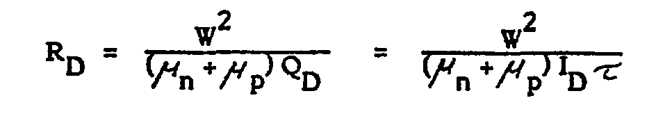
Il y a donc intérêt, pour que la résistance en direct RD soit minimale, à ce que τ soit maximal. Or, on sait que la durée de vie τ est influencée négativement par les contraintes mécaniques entre zones très dopées P et N et la zone I peu dopée.It is therefore advantageous, for the direct resistance R D to be minimum, for τ to be maximum. However, it is known that the lifetime τ is negatively influenced by the mechanical stresses between heavily doped P and N zones and the weakly doped zone I.
Il importe donc de rechercher:
- - des transitions P-I et I-N abruptes, afin d'optimiser le fonctionnement de la diode dans le cas où la tension inverse est supérieure à la tension de perçage,
- - une résistivité finale préel la plus élevée possible, afin de réduire les pertes dans le cas où la tension inverse est inférieure à la tension de perçage,
- - une durée de vie la plus élevée possible, afin de réduire la résistance en direct RD.
- - abrupt PI and IN transitions, in order to optimize the operation of the diode in the case where the reverse voltage is greater than the drilling voltage,
- - the highest possible preel final resistivity, in order to reduce losses in the case where the reverse voltage is lower than the drilling voltage,
- - the longest possible service life, in order to reduce the direct resistance R D.
Ces objectifs sont atteints avec la diode PIN selon l'invention, qui est représentée en figure 5, sur laquelle la structure de la diode est rapportée en dessous de l'axe des abscisses, tandis que les niveaux de dopage sont rapportés au-dessus de ce même axe, afin de ne pas confondre les jonctions entre couches et les niveaux de transitions abruptes, qui se superposeraient.These objectives are achieved with the PIN diode according to the invention, which is shown in FIG. 5, on which the structure of the diode is reported below the x-axis, while the doping levels are reported above this same axis, so as not to confuse the junctions between layers and the levels of abrupt transitions, which would overlap.
La diode PIN selon l'invention est réalisée - de façon collective bien entendu - à partir d'une tranche de silicium parfaitement rodée et donc d'épaisseur bien controlée, qui correspond à la zone I repérée 8. Cette tranche n'est pas intentionnellement dopée, c'est-à-dire que son niveau d'impuretés se situe aux environs de 1012.The PIN diode according to the invention is produced - collectively of course - from a perfectly ground silicon wafer and therefore of well controlled thickness, which corresponds to zone I marked 8. This wafer is not intentionally doped, that is to say that its level of impurities is around 1012.
Sur ce substrat sont réalisées deux couches épitaxiées, une couche P 9 sur une face du substrat et une couche N 10 sur l'autre face. Bien entendu, les précautions habituelles à l'homme de l'art sont prises pour que la seconde épitaxie ne détériore pas la couche réalisée au cours de la première épitaxie. Le procédé utilisé pour les épitaxies n'intervient pas dans le résultat: elle peuvent être à pression atmosphérique ou sous basse pression.On this substrate, two epitaxial layers are produced, a layer P 9 on one side of the substrate and a
Ce qui fait l'originalité de la diode selon l'invention est que les niveaux de dopage, au cours des épitaxies, sont de 10 à 100 fois moindres que les niveaux de dopage habituels: ils sont au niveau de 5.1016 à 5.1018 at.cm-3, alors que l'on connait des diodes épitaxiées mais à des niveaux supérieurs à 1019 at.cm-3, ce qui introduit des contraintes mécaniques entre couches très dopées et zone I, et donc diminue la durée de vie τ, comme cela a été dit.What makes the diode according to the invention original is that the doping levels, during the epitaxies, are 10 to 100 times less than the usual doping levels: they are at the level of 5.1016 to 5.1018 at.cm -3, while we know of epitaxial diodes but at levels higher than 1019 at.cm -3 , which introduces mechanical stresses between highly doped layers and zone I, and therefore decreases the lifetime τ, like this has been said.
Il est utile de terminer chaque opération d'épitaxie par un court surdopage à 1019 at.cm-3, afin de créer de fines couches de 1 ou 2 micromètres, 11 du côté P et 12 du côté N, destinées à améliorer le contact ohmique pris sur ces couches. Cette opération est bien connue, et ce léger surdopage n'interfère pas avec l'invention, puisqu'il concerne les prises de contact et non pas les transitions P-I et I-N. Ce mince surdopage peut aussi être réalisé par diffusion courte.It is useful to end each epitaxy operation with a short overdoping at 10 19 at.cm -3 , in order to create thin layers of 1 or 2 micrometers, 11 on the P side and 12 on the N side, intended to improve contact. ohmic caught on these layers. This operation is well known, and this slight overdoping does not interfere with the invention, since it relates to making contact and not the PI and IN transitions. This thin overdoping can also be achieved by short diffusion.
La partie supérieure de la figure 5 met en évidence les transitions abruptes: le substrat 8, qui constitue maintenant la zone I, de longueur bien définie W, est non dopé, à un niveau de 2.1012 par exemple, représenté par la droite 13. Le niveau de dopage des couches P 9 et N 10 est représenté par les droites horizontales 14 et 15, aux environs de 5.1016-5.1018. Etant donné que le taux de dopage a été maintenu constant pendant toute la durée des épitaxies - sauf le surdopage final pour les contacts - et qu'il n'y a pas diffusion d'impuretés dans le substrat, ou zone I, les transitions P-I et I―N sont abruptes et représentées respectivement par les droites 16 et 17, quasi verticales sur ce graphique.The upper part of FIG. 5 highlights the abrupt transitions: the substrate 8, which now constitutes the zone I, of well defined length W, is undoped, at a level of 2.1012 for example, represented by the
A titre d'exemple non limitatif, considérons une diode PIN pour laquelle:
- W = 100 µm
- S = 500 x 500 µm
- ID 100 mA
- po = 4000 Ω/cm
- RD = 0,5 Ω
- W = 100 µm
- S = 500 x 500 µm
- I D 100 mA
- p o = 4000 Ω / cm
- R D = 0.5 Ω
Si on désire que les résistances "parasites" Rp et RN soient au maximum égales au dixième de la résistance en direct RD 
- CN = 2.1017 at.cm-3
- Cp = 1018 at.cm-3
- soit une résistivité de 0,06 Ω/cm pour chaque couche épitaxiée. Sur la figure 5, le niveau de dopage de la couche P 9 est effectivement voisin de 1018, tandis que le niveau de la couche N 10 est un peu supérieur à 1017.
- CN = 2.10 17 at.cm-3
- Cp = 1 0 18 at.cm-3
- or a resistivity of 0.06 Ω / cm for each epitaxial layer. In FIG. 5, the doping level of the P layer 9 is effectively close to 10 18 , while the level of the
N layer 10 is slightly greater than 1017.
La diode PIN selon l'invention a beaucoup moins de contraintes mécaniques que les diodes selon l'art connu, puisque les couches P et N sont moins dopées: par conséquent, la durée de vie τ des porteurs de charges est plus élevée, ce qui diminue la résistance en direct RD.The PIN diode according to the invention has much less mechanical stress than the diodes according to the known art, since the P and N layers are less doped: consequently, the lifetime τ of the charge carriers is higher, which decreases direct resistance R D.
Enfin, ce qui n'est pas négligeable du point de vue du rendement de fabrication industrielle, la découpe des diodes dans la tranche de silicium est de meilleur rendement, puisqu'il y a moins de contraintes mécaniques entre les couches de la diode PIN.Finally, which is not negligible from the point of view of industrial production efficiency, the cutting of the diodes in the silicon wafer is of better efficiency, since there are less mechanical stresses between the layers of the PIN diode.
La diode PIN selon l'invention est d'usage général, mais elle est surtout utilisée en hyperfréquences.The PIN diode according to the invention is of general use, but it is especially used in microwave.
Claims (2)
Applications Claiming Priority (2)
| Application Number | Priority Date | Filing Date | Title |
|---|---|---|---|
| FR8502766A FR2578101B1 (en) | 1985-02-26 | 1985-02-26 | PINE HYPERFREQUENCY DIODE WITH ABRUPT TRANSITIONS |
| FR8502766 | 1985-02-26 |
Publications (2)
| Publication Number | Publication Date |
|---|---|
| EP0193462A1 EP0193462A1 (en) | 1986-09-03 |
| EP0193462B1 true EP0193462B1 (en) | 1989-03-29 |
Family
ID=9316635
Family Applications (1)
| Application Number | Title | Priority Date | Filing Date |
|---|---|---|---|
| EP19860400379 Expired EP0193462B1 (en) | 1985-02-26 | 1986-02-21 | High frequency pin-type diode with abrupt junctions |
Country Status (3)
| Country | Link |
|---|---|
| EP (1) | EP0193462B1 (en) |
| DE (1) | DE3662629D1 (en) |
| FR (1) | FR2578101B1 (en) |
Families Citing this family (5)
| Publication number | Priority date | Publication date | Assignee | Title |
|---|---|---|---|---|
| EP0277336A1 (en) * | 1987-01-13 | 1988-08-10 | BBC Brown Boveri AG | Method of making a fast semiconductor device |
| GB9520324D0 (en) * | 1995-10-05 | 1995-12-06 | Secr Defence | Improved auger suppressed device |
| USRE38582E1 (en) | 1995-10-05 | 2004-09-14 | Qinetiq Limited | Semiconductor diode with suppression of auger generation processes |
| DE10031461B4 (en) | 2000-06-28 | 2006-06-29 | Infineon Technologies Ag | High-voltage diode |
| EP2996152B1 (en) * | 2014-09-15 | 2017-03-15 | ABB Schweiz AG | High frequency power diode and method for manufacturing the same |
Family Cites Families (3)
| Publication number | Priority date | Publication date | Assignee | Title |
|---|---|---|---|---|
| JPS5645081A (en) * | 1979-09-19 | 1981-04-24 | Toshiba Corp | Low-loss diode |
| JPS5860577A (en) * | 1981-10-07 | 1983-04-11 | Hitachi Ltd | Semiconductor device |
| DE3328521C2 (en) * | 1983-08-06 | 1985-11-14 | SEMIKRON Gesellschaft für Gleichrichterbau u. Elektronik mbH, 8500 Nürnberg | Rectifier diode for high reverse voltage |
-
1985
- 1985-02-26 FR FR8502766A patent/FR2578101B1/en not_active Expired
-
1986
- 1986-02-21 EP EP19860400379 patent/EP0193462B1/en not_active Expired
- 1986-02-21 DE DE8686400379T patent/DE3662629D1/en not_active Expired
Also Published As
| Publication number | Publication date |
|---|---|
| EP0193462A1 (en) | 1986-09-03 |
| DE3662629D1 (en) | 1989-05-03 |
| FR2578101B1 (en) | 1987-10-09 |
| FR2578101A1 (en) | 1986-08-29 |
Similar Documents
| Publication | Publication Date | Title |
|---|---|---|
| EP0199424B1 (en) | Planar semiconductor device with a guard ring structure, family of such devices and method of manufacture | |
| EP3384537B1 (en) | Optoelectronic apparatus comprising tridimensional semiconductor structures in axial configuration | |
| EP0545808B1 (en) | Optoelectronic device with very low series resistance | |
| EP1073110A1 (en) | Method of manufacturing unipolar devices | |
| EP0236189B1 (en) | Monolithic semiconductor structure of a heterojunction bipolar transistor and a laser | |
| FR2744836A1 (en) | PROGRESSIVE CONCENTRATION EPITAXIAL SUBSTRATE FOR RESURF-DIFFUSED SEMICONDUCTOR DEVICE | |
| FR2755794A1 (en) | HIGH VOLTAGE POWER SCHOTTKY DIODE HAVING A BARRIER METAL MADE OF ALUMINUM AND SPREADED FROM THE FIRST DIFFUSED RING | |
| EP0006474A1 (en) | Method of compensating for the voltage coefficient of ion-implanted or diffused semiconductor resistors | |
| EP0368768B1 (en) | Process for making a fast diode, and fast diode obtained by that process | |
| EP0193462B1 (en) | High frequency pin-type diode with abrupt junctions | |
| EP0001728A1 (en) | Light emitting and receiving diode, in particular for optical telecommunication | |
| EP0090722B1 (en) | Fast diode | |
| FR2554276A1 (en) | REFERENCE DIODE FOR INTEGRATED CIRCUIT AND METHOD FOR MANUFACTURING THE SAME | |
| EP0082787B1 (en) | Photodiode with separated absorption and avalanche regions | |
| FR2556882A1 (en) | FAST SEMICONDUCTOR COMPONENT, IN PARTICULAR DIODE PIN HIGH VOLTAGE | |
| EP3792982A1 (en) | Electronic power device with super-junction | |
| EP3973579B1 (en) | Optoelectronic device with light-emitting diodes a doped region of which incorporates an external segment based on aluminium and gallium nitride | |
| FR2640813A1 (en) | INTEGRATED CIRCUIT HAVING A VERTICAL TRANSISTOR | |
| FR2570545A1 (en) | SEMICONDUCTOR DEVICE WITH UNDERGROUND RESISTANCE | |
| FR2587842A1 (en) | NORMALLY LOCKED SEMICONDUCTOR POWER DEVICE FOR HIGH VOLTAGES AND WITH MODULATED CONDUCTION RESISTANCE | |
| EP0454248B1 (en) | Integrated circuit comprising a multiple collector lateral transistor | |
| EP0032069B1 (en) | Method to adjust the temperature coefficient of a reference diode and a reference diode so adjusted | |
| EP0987751A1 (en) | Isolation wall between power devices | |
| FR2721439A1 (en) | Optical semiconductor elements and methods of manufacturing thereof | |
| FR2601504A1 (en) | Semiconductor device including a transistor for integrated injection logic |
Legal Events
| Date | Code | Title | Description |
|---|---|---|---|
| PUAI | Public reference made under article 153(3) epc to a published international application that has entered the european phase |
Free format text: ORIGINAL CODE: 0009012 |
|
| AK | Designated contracting states |
Kind code of ref document: A1 Designated state(s): DE GB NL |
|
| 17P | Request for examination filed |
Effective date: 19860919 |
|
| 17Q | First examination report despatched |
Effective date: 19880224 |
|
| GRAA | (expected) grant |
Free format text: ORIGINAL CODE: 0009210 |
|
| AK | Designated contracting states |
Kind code of ref document: B1 Designated state(s): DE GB NL |
|
| REF | Corresponds to: |
Ref document number: 3662629 Country of ref document: DE Date of ref document: 19890503 |
|
| RAP4 | Party data changed (patent owner data changed or rights of a patent transferred) |
Owner name: THOMSON-CSF |
|
| GBT | Gb: translation of ep patent filed (gb section 77(6)(a)/1977) | ||
| PLBE | No opposition filed within time limit |
Free format text: ORIGINAL CODE: 0009261 |
|
| STAA | Information on the status of an ep patent application or granted ep patent |
Free format text: STATUS: NO OPPOSITION FILED WITHIN TIME LIMIT |
|
| 26N | No opposition filed | ||
| PGFP | Annual fee paid to national office [announced via postgrant information from national office to epo] |
Ref country code: DE Payment date: 19930121 Year of fee payment: 8 |
|
| PGFP | Annual fee paid to national office [announced via postgrant information from national office to epo] |
Ref country code: GB Payment date: 19930125 Year of fee payment: 8 |
|
| PGFP | Annual fee paid to national office [announced via postgrant information from national office to epo] |
Ref country code: NL Payment date: 19930228 Year of fee payment: 8 |
|
| PG25 | Lapsed in a contracting state [announced via postgrant information from national office to epo] |
Ref country code: GB Effective date: 19940221 |
|
| PG25 | Lapsed in a contracting state [announced via postgrant information from national office to epo] |
Ref country code: NL Effective date: 19940901 |
|
| NLV4 | Nl: lapsed or anulled due to non-payment of the annual fee | ||
| GBPC | Gb: european patent ceased through non-payment of renewal fee |
Effective date: 19940221 |
|
| PG25 | Lapsed in a contracting state [announced via postgrant information from national office to epo] |
Ref country code: DE Effective date: 19941101 |