EP0190743A2 - Control signal generation circuit for wireless remote control signal transmitter - Google Patents
Control signal generation circuit for wireless remote control signal transmitter Download PDFInfo
- Publication number
- EP0190743A2 EP0190743A2 EP86101476A EP86101476A EP0190743A2 EP 0190743 A2 EP0190743 A2 EP 0190743A2 EP 86101476 A EP86101476 A EP 86101476A EP 86101476 A EP86101476 A EP 86101476A EP 0190743 A2 EP0190743 A2 EP 0190743A2
- Authority
- EP
- European Patent Office
- Prior art keywords
- key
- output terminals
- custom code
- scan
- terminal
- Prior art date
- Legal status (The legal status is an assumption and is not a legal conclusion. Google has not performed a legal analysis and makes no representation as to the accuracy of the status listed.)
- Granted
Links
Images


Classifications
-
- H—ELECTRICITY
- H03—ELECTRONIC CIRCUITRY
- H03M—CODING; DECODING; CODE CONVERSION IN GENERAL
- H03M11/00—Coding in connection with keyboards or like devices, i.e. coding of the position of operated keys
- H03M11/20—Dynamic coding, i.e. by key scanning
Definitions
- the present invention relates to a control signal generation circuit used in a wireless remote control signal transmitter for controlling the circuit operation of an instrument such as a television receiver, a video tape recorder, a toy, an air condisioner, etc., and more particularly to a custom code generation circuit employed in such a signal transmitter, which generates a custom code used for selecting and designating the instrument to be controlled among various ones.
- a remote control signal transmitter generates a data code for controlling the operation of a controlled instrument in response to actuated or operated key or keys, wherein a semiconductor integrated circuit device (called hereinafter as an "IC") is widely used to form the data code responsive to the operated key and modulate the data code to transmit it by means of infrared rays, electromagnetic waves or supersonic waves.
- the remote control signal transmitter also generates a custom code in addition to the generation of the data code, the custom code being alloted to the instrument to be controlled in order that only that instrument responds to the code data. By the custom code, undesired instruments are prevented from responding to the data code.
- a custom code setting terminal (called hereinafter as a "CCS" terminal) is provided to the remote control IC and key scan signals outputted from key scan output terminals are supplied selectively to the CCS terminal to obtain a custom code, as disclosed in United Stated Patent No. 4,412,218. More specifically, the scan signals are outputted cyclically from the key scan output terminals to detect the operated key. Therefore, by coupling the selected key scan output terminal or terminals to the CCS terminal and detecting the level at the CCS terminal in synchronism with the generation timing of the scan signals, a pulse train having the combination of the data "1" and "0" is obtained. The custom code is derived from the pulse train.
- Such a remote control IC requires a CCS terminal.
- An I C having a smaller number of external terminals is manufactured more cheaply, resulting in decreasing the cost of.a signal transmitter.
- an object of the present invention is to provide a control signal generation circuit generating a plurality of custom codes without increase in number of terminals.
- Another object of the present invention is to provide a control signal generation circuit which can generate a larger number of custom codes without any increase in number of a custom code setting terminal of prior art.
- a control signal generation circuit comprises a plurality of key output terminals coupled with a key matrix, means for generating scan signals from the key output terminals, impedance means for connecting selected one or ones of the key output terminals to a potential source, means coupled to the key output terminals for detecting a potential at each key output terminal during a period other than the scan signal generation period of the scan signal generation means, and means for producing a custom code in response to an output of the detecting means.
- the key output terminals are also used as custom code selection terminals.
- the detecting means detects the potential at each key output terminal during a period other than the scan signal generation period.
- the selected key output terminal or terminals are coupled to the potential source. Assuming that the detection level'at the terminal connected to the potential source is a.logic "1" and that at the terminal non-connected to the source is a logic "0", the combination of the logics "1" and "0" is thus obtained. This combination is varied by the selection and/or the number of the key output terminal or terminals coupled to the potential source. As a result, a plurality of custom codes are derived without a custom code selection terminal which was required in the prior art.
- the present invention does not exclude the custom code producing means utilizing the CCS terminal, but the present invention can be applied to the remote control IC with the CCS terminal. In this case, an extremely large kinds of custom codes are produced by using a remote control IC having the same terminal number as the prior art.
- a remote control signal transmitter generates a custom code and a key data_code representative of information of an operated key and outputs them as infrared rays by means of an infrared ray diode 14.
- the custom code and key data code are produced by a remote control IC 1 from its output terminal OUT and then supplied to a drier circuit 13 to drive the diode 14.
- a key matrix 15 which is used to command the change in operation of an instrument to be remote-controlled.
- the key matrix 15 includes four row lines a to d, eight column lines e to l, and thirty-two key switches KS disposed at the respective intersections of the row and column lines.
- the row lines a to d are connected to key input terminals KI 0 to KI 3 of the IC 1, respectively, and the column lines e to 1 are connected to key output terminals KO 0 to K0 7 of the IC 1, respectively.
- the selected key output terminals (in this embodiment, the first, fourth and eighth key output terminals KO 0 , K0 3 and K0 7 ) are connected to a power voltage source (not shown) via resistors 16, 17 and 18, respectively.
- the power voltage source is also connected to a power terminal V DD of the IC 1.
- the IC 1 has another power terminaly V SS which is in turn connected to a ground.
- all the key output terminals KO 0 to KO 7 of the IC 1 assume a high level.
- any one of the key input terminals KI 0 to KI 3 is thereby supplied with the high level.
- This high level is detected by a key input circuit 6, and the circuit 6 then supplies an oscillation-enable signal to an oscillator 3.
- the oscillator 3 thus oscillates at a frequency determined by a resonant element 2 such as a crystal or a ceramic resonator connected between terminals OSC 1 and OSC 2 .
- the oscillation signal of the oscillator 3 is frequency-divided by a divider 4 to a predetermined frequency signal, and in response to this predetermined frequency signal a timing generator 5 supplies timing signals to the key input circuit 6, a key output circuit 7 and a controller 11.
- the key output circuit 7 responds to the timing signal from the timing generator 5 and a control signal from the controller 11 and outputs cyclically to the key output terminals KO to KO 7 key scan signals used for detecting the operated key switch, but before this scan signal output operation, a custom code read operation is attained for reading-out the custom code alotted to the instrument to be controlled by this signal transmitter.
- a level detection circuit 8 is provide to detect the level at each key output terminal KO.
- the input stage of the level detection circuit 8 as shown in Fig.'2 includes an N-channel MOS transistor Q 3 connected between each key output terminal and the ground and supplied at.its.gate with a clock signal ⁇ 3 and P-channel and N-channel MOS transistors Q 4 and Q 5 constituting an inverter 30 which receives the level at each key output terminal KO.
- An output stage of the key output circuit 7 is also shown in Fig.
- the first key output terminal KO is represented, and therefore this terminal is connected to the power V DD via the resistor 16.
- Fig. 3 input stage of the key input circuit 6 is shown.
- Each of the key input terminals KO 0 to KI 3 is connected to the ground via a pull-down resistor 19 and an N-channel MOS transistor Q 8 receiving at its gate a clock signal ⁇ 4 , and further connected to the gates of P-channel and N-channel MOS transistors Q 6 and Q 7 .
- These transistors Q 6 and Q 7 are connected in series between the power terminals to constitute an inverter 31.
- the clock signal ⁇ 2 supplied to the transistor Q 2 which is provided for the first key output terminal KO 0 is inverted into the low level as shown in Fig. 4.
- the gates of transistors Q 2 provided.for.the remaining key output terminals KO 1 to KO 7 are maintained at the high level.
- the clock signal ⁇ 3 is inverted into the low level in synchronism with the invertion of the clock ⁇ 2 .
- the inversion of the clock signal ⁇ 3 occurs only for the first key output terminal KO 0 and does not occur for the remaining key output terminals KO 1 to KO 7 .
- the transistor Q 3 connected to the first key output terminal KO 0 is thus turned ON, so that the resistance-divided voltage appears at the first key output terminal KO 0 , which is represented by a reference numeral 20 in Fig. 4 and determined by the conducting resistance of the transistor Q 3 and the resistor 16.
- the impedance between the first key output terminal KO 0 and the ground would be lowered due to the pull-down resistor 19, so that the above-mentioned resistance-divided voltage become close to the low level.
- the resistor 16 does not achieve its function.
- the clock signal ⁇ 4 takesthe low level in synchronium with the inversion of the clock signal ⁇ 2 , so that the transistors Q 8 provided for all the key input terminals KI 0 to KI 4 are turned OFF.
- the pull-down resistor 19 is thereby disconnected from the ground.
- the resistance-divided voltage at the key output terminal KO 9 . is determined by the resistor 16 and the conducting resistance of the transistor Q 3 .
- the conducting resistance of the transistor Q 3 is designed such that the resistance-divided voltage becomes larger than the logical threshold voltage of.the inverter 30. Accordingly, the output voltage V 30 of the inverter 30 takes the low level as shown in Fig. 4. As a result, the level detection circuit detects that the first key output terminal KO 0 is connected to the power terminal V DD via the resistor 16 and supplies to a custom code register 10 a data "1", for example.
- the clock signals ⁇ 2 , ⁇ 3 and ⁇ 4 thereafter invert to the high level, the low level and the high level, respectively, so that the first key output terminal KO 0 and the output voltage V 30 of the inverter 30 takes the low level and the high level, respectively.
- the clock signal ⁇ 2 supplied.to the transistor Q 2 provided for the second key output terminal KO 1 is inverted to the low level.
- the clock signals ⁇ 3 and ⁇ 4 are changed to.the high level and the low level, respectively.
- the level detection circuit 8 thereby supplies a data "0" to the custom code resistor 10.
- the above-mention operation is continued for the remaining key output terminals KO 2 to KO 7 .
- the voltage exceeding the threshold.voltage of the inverter 30 appears at the first, fourth and eighth key output terminals KO O , KO 3 and KO 7 due to the resistors 16 to 18, as represented as a custom code read cycle in Fig. 6.
- the level detection circuit 8 detects the level at each key output terminal and supplies to"the register 10 the data corresponding to the detected level.
- the registor 10 thus stores data "10010001" therein at a time when the custom code read cycle is completed.
- the data stored in the register 10 is used as a custom code.
- the IC 1 is brought into an operated key switch detection cycle, i.e. a key scan signal output cycle.
- the clock signals ⁇ 1 and ⁇ 2 both takes the low level to turn the transistors Q 1 and Q 2 ON and OFF, respectively, as shown in Fig. 5.
- the first key output terminal KO 0 is thereby .raised to the high level.
- the remaining key output terminals KO to KO 7 are held at the low level.
- the clock signal ⁇ 3 assumes the low level to maintain the transistor Q 3 in the nonconducting state.
- the clock signals ⁇ 4 is inverted into the low level in synchronism with the clock signals ⁇ 1 and ⁇ 2 to disconnect the pull-down resistor 19 in the key input circuit 6 from the ground.
- the clock signal ⁇ 4 may be held at the high level, but in that case the . conducting resistance of the transistor Q 1 is required to be sufficiently smaller than the resistor 19..
- the operated key switch is one of the key switches KS disposed on the first column line e
- one of the key input terminals KI 0 to KI 3 is supplied with the high level.
- the input terminal KI supplied with the high level depends on the operated key.
- the inverter 31 .produces its output voltage V 31 having the low level.
- the output voltage V 31 of the inverter 31 does not change.
- the clock signals ⁇ 1 and ⁇ 2 thereafter return to the high level, so that the first key output terminal KO is inverted to the low level.
- the key output circuit 7 includes a counter (not shown) therein, and the content thereof changes by.the fact that which key output terminal KO outputs the key scan signal.
- the key input circuit 6 also includes a counter therein, and its count value varies by the fact that which key input terminal is supplied with the high level signal.
- the contents of these counters in the key input and output circuits 6 and 7 are employed as a key data code corresponding to the operated key switch and supplied to a key data register 9 to be stored therein.
- the level detection circuit 8 is in the non-activated state; and therefore the circuit 8 does not produce any its output signal.
- the custom code read operation and the operated key detection (the.scan signal output) operation are carried out twice and the custom codes and key data codes obtained in the respective cycles are then compared with each other in order to prevent an error custom code and an error key data code.
- the custom code and key data code stored respectively in the register 9 and 10 are read-out in serial and in that order by the controller 11.
- the controller 11 performs the well-know Pulse-Position-Modulation (PPM) with respect to the read-out codes, and. further produces the inverted codes of the custom and key data codes.
- the inverted codes are also subjected to the PPM.
- the modulated non-inverted custom code, inverted custom code, non-inverted key data code and inverted key data code are supplied in that order to an output control circuit 12.
- the circuit 12 is also supplied with a signal of 38 KHz which is derived from the divider 4, and this signal is superposed on the respective codes as a carrier wave.
- the output of the output control circuit 12 is supplied to the-output terminal OUT of the IC 1 and further introduced into the drive circuit 13.
- the circuit 13 controls the..ON and OFF states of the infrared ray diode 14 in response to the signal from the output terminal oum.
- the custom code and the key data code are transmitted by means of infrared rays.
- the instrument to be remote-controlled receives the command signal transmitted via the infrared rays and detects at first the custom code.
- the custom code.thus detected is then compared with that allotted to the instrument.
- the instrument introduces the key data code and then performs the corresponding operation.
- the custom code for designing the instrument to be controlled is set without providing the custom code setting terminal, and further its kinds are changeable.
- the resistors 16 to 18 are used for setting the custom code, and diodes which are relatively expensive, are not recessary.
- F i g . 7 shows a second embodiment of the present invention.
- a custom code ROM (Read-Only-Memory) 43 memorizing eight kinds of custom codes is provided in a remote-control IC 100, and one of them is selected by connecting either one of eight key output terminals KO 0 to K0 7 to the power terminal V DD via a resistor 40.
- the resistor 40 is connected in this embodiment between the fifth key output terminal and the power terminal V DD . Accordingly, as has been mentioned with reference to Figs. 2 and 4, when the transistors Q 2 and Q3 provided for the fifth key output terminal K0 4 are turned OFF and ON, respectively, the voltage exceeding the threshold level of the inverter 30 appears at that terminal KO 4 .
- the level detection circuit 8 thereby produces data "1", for example. Before this and after this, the circuit 8 produces data "0".
- the output data of the circuit 8 are supplied'to an address generator 42.
- the generator 42 generates an address signal responsive to the output of the circuit 8 and then supplied it to the custom code ROM 43.
- the custom code stored in the fifth address of the ROM 43 is read-out and then supplied to the custom code register 10,
- the address varies by changing the key output terminal KO coupled to the power terminal V DD , and the custom code stored in the register 10 is thereby changed. Also in this embodiment, the custom code setting terminal is not required. If a plurality of key output terminals are coupled to the power terminal V DD , many kinds of address signals more than eight are generated. In accordance this, the memory capacity of the ROM can be increase to set a larger number of custom codes.
- Fig. 8 shows the third embodiment of the present invention.
- a custom code setting terminal (CCS terminal) is provided on the IC 200.
- a selected first group of the key output terminals (KO O , K0 4 and KO 7 in this embodiment) is coupled to the power terminal V DD via resistors 41, 42 and 43, respectively, and a selected second group of the key output terminals (in this embodiment, KOO , KO 1 , K02 and KO 5 ) is coupled to the CCS terminal via diodes 44, 45, 46 and 47, respectively.
- KOO , KO 1 , K02 and KO 5 is coupled to the CCS terminal via diodes 44, 45, 46 and 47, respectively.
- the output stage of the key output circuit 7 and the input stage of the key detection circuit 8 have the same circuit constructions as those of Fig. 2, but the clock signals ⁇ 1 to ⁇ 3 supplied to the respective transistors are different from those of Fig. 4, as shown in Fig. 9. More particularly, when the oscillator 3 starts to oscillate, all the key output terminals KO O to K0 7 take the low level, followed by the inversions of the clock signal ⁇ 1 and ⁇ 2 supplied to the transistors Q 1 and Q 2 provided for the first key output terminals KO O . The transistors Q 1 and Q 2 are thereby turned ON and OFF, respectively, the first key output terminal KO 0 is changed to the high level.
- the clock signal ⁇ 3 is in the low level.
- the terminal CCS since the first key output terminal KO 0 is connected to the CCS terminal via the diode 44, the terminal CCS is supplied with the high level.
- the key input circuit 6 is coupled to the CCS terminal and detects the high level at that terminal to produce data "1", for example. This data is supplied to a first custom code register 10-1. If the diode 4.4 is not provided, the CCS terminal is in the low level, and therefore the register 10-1 receives data "0".
- the inverter 30 connected to the first key output terminal KO 0 produces the low level as its output voltage V 30 , but the level detection circuit 8 rejects the output voltage V 30 by a control signal from the controller 11.
- the diode read operation is carried out when all of the clock signals ⁇ 1 , ⁇ 2 and ⁇ 3 are in the low level, as shown in F ig. 9.
- the clock signals ⁇ 1 and ⁇ 3 are both inverted into the high level to turn the transistor Q 1 and Q 3 OFF and ON, respectively.
- the first key output terminal KO O is connected via the resistor 41 to the power terminal V DD . Therefore, the resistance-divided voltage determined by the resistor 41 and the conducting resistance of the transistor Q 3 appears at the first key output terminal KO 0 , Since this divided voltage exceeds the threshold voltage of the inverter 30, the output voltage.V 30 is held at the low level as shown in Fig. 9.
- the level datection circuit 8 takes up the output voltage V 30 at this time and supplies data "1" to a second custom code register 10-2.
- the divided voltage appearing at the terminal KO 0 does not make the diode 44'conductive, and hence the CCS terminal assumes the low level.
- the divided voltage may turn the diode 44 ON, and in that case, the key input circuit 6 is required to be in the non-activated state by another control signal from the controller 11. As a result, a resistor read-out operation is carried out.
- the diode read-out operation and the.resistor read-out operation are then attained with respect to the second key output terminal KO 1 .
- This terminal KO 1 is connected to the CCS terminal via the diode 45, but no resistor is inserted between the terminals KO 1 and V DD . Therefore, data "1" is stored into the first custom code register 10-1, and data "0" is stored in the'second custom code register 10-2.
- the above-mentioned operations are carried out to the eighth key output terminal KO 7 , so that a timing chart represented as a custom code read operation in F ig. 10 is obtained.
- the CCS terminal is supplied with the high level in sycnhronism the signal output from the those key output terminals.
- the resistors 41, 42 and 43 are present between the power terminal V DD and the first, fifth and eight terminals KO 0 , KO 4 and KO 7 , respectively, the divided voltage appears at those terminals.
- the first custom code register 10-1 stores data "11100100" therein
- the second custom code register 10-2 stores data "10001001" therein.
- the operated key detection operation is thereafter carried out in a.similar manner to that described with reference to the first embodiment, followed by the output of the custom and key data codes.
- the data stored in the first and second custom code register 10-1 and 10-2 are outputted without any modification. That is, as shown in Fig. 11A, in the custom code composed of sixteen bits, a custom code (1) composed of Ci-bit to C 8 -bit is constructed by the data "11100100" of the first register 10-1, and a.custom code (2) composed of C 1 '-bit to C 8 '-bit is constructed by the data "10001001" of the second register 10-2.
- a key code data composed of K 1 -bit to K 8 -bit and its inverted key code data (K ⁇ 1 -bit to K ⁇ 8 -bit) are outputtted.
- a transmission- enable signal called as a leader pulse is generated.
- the second custom code output method is shown in Fig. 11B.
- the data "11100100" stored in the first register 10-1 is used as the custom code (1) composed of C l -bit to C 8 -bit.
- the customer code (2) composed of C 1 '-bit to C 8 '-bit.
- the custom code (2) is obtained by inverting the data stored in the bits in the first register 10-1 except for the bits corresponding to those in the second register 10-2 storing the data "1".
- the custom code (2) takes data "10010010".
- the third custom code output method is such that a custom code ROM 48 represented by a dotted line in Fig. 8 is provided in IC 200 and the data stored in the ROM 48 is utilized along with the data stored in the registers 10-1 and 10-2.
- the custom code ROM 48 is a sixteen bits construction and stores data "0001000101100000".
- the controller 11 reads out the data stored in the registers 10-1 and 10-2 as well as the data stored in the ROM 48, and obtains a first logical ORed data of the first half eight-bits data of the ROM 48 and the data of the register 10-1 and a second logical ORed data of the Second half eight-bits data of the ROM 48 and the data of the register 10-2.
- the first and second logical ORed data are "11110101” and "11101001", respectively, in consequence.
- the controller 11 outputs the first logical ORed data as the custom code (1).
- the custom code (2) is obtained by inverting.the data stored in the bits in the first logical ORed data except for the bits corresponding to those in the second logical ORed data storing the data "I". Accordingly, the custom codes (1) and (2) assume the data "11110101" and "11100011", respectively.
- the signal transmitter according to this embodiment provides an extremely large kinds of custom codes by employing a remote-control IC haying the same terminal number as the prior art.
- the data stored in the second register 10-2 may be used as a custom code (1).
- Fig. 12 shows a fourth embodiment of the present invention.
- the custom code setting function usirig the CCS terminal and that using the level detection circuit 8 are provided similarly to the third embodiment, but the custom code setting function using the CCS terminal is different in its construction from that of the third embodiment.
- the CCS terminal is connected to only one of the first to eighth key output terminals KO 0 to KO 7 . (in this embodiment, the fourth key output terminal KO 3 ).
- the custom code read operation is carried out similarly to the third embodiment.
- the second, fifth and sixth key output terminals KO 1 ,KO 4 and KO 5 are connected to the power terminal V DD via resistors 52, 53, and 54, respectively. Therefore, the second register 10-2 stores data "01001100" therein.
- the CCS terminal receives the high level only when the terminal KO 3 is at the high level.
- an address generator 51 coupled to the CCS terminal generates an address signal that selects the fourth address of a custom code ROM 50.
- the ROM 50 memorizes eight kinds of custom codes. The data read-out from the ROM 50 is supplied to the first register 10-1.
- one of eight kinds of custom codes is selected by connecting only one of the key output terminals KO to the CCS terminal, and a greater number of custom codesare further produced by the resistors 52 to 54.
- a fifth embodiment of the present invention is shown in Fig. 13.
- the detection circuit 8 detects the level at the seventh and eighth key output terminals XO 6 and KO 7 .
- the output of the circuit 8 is supplied to an address generator 61, and one address of. a custom code ROM 62 is thereby selected.
- the ROM 62 stores four kinds of custom codes therein. Each of custom codes is a five-bits construction.
- the CCS terminal is connected either one of the first to eighth key output terminals KO 0 to KO 7 , and in response to the connecting location, a code generation circuit 60 generates data camposed of three-bits and represented by the following Table-2; The three-bits data generated by the generator 60 is supplied to the register 63 and stored in its former three-bits.
- the custom code register 63 storing a custom code of an eight-bits construction.
- the controller 11 thereafter processes the signal, as has been already mentioned.
- the present invention is not limited to the aforementioned embodiments, but can be modified and changed without departing from the scope and spirit of the invention.
- the selected key output terminal or terminals may be connected to the ground potention, and in that case all the logic level mentioned above are inverted. It is also possible to connect the selected key output terminal directly to the potential source. In this case, the conducting resistance of the transistor Q 3 is preferrably made large in order to reduce a power consumption.
Landscapes
- Engineering & Computer Science (AREA)
- Theoretical Computer Science (AREA)
- Selective Calling Equipment (AREA)
- Lock And Its Accessories (AREA)
Abstract
Description
- The present invention relates to a control signal generation circuit used in a wireless remote control signal transmitter for controlling the circuit operation of an instrument such as a television receiver, a video tape recorder, a toy, an air condisioner, etc., and more particularly to a custom code generation circuit employed in such a signal transmitter, which generates a custom code used for selecting and designating the instrument to be controlled among various ones.
- A remote control signal transmitter generates a data code for controlling the operation of a controlled instrument in response to actuated or operated key or keys, wherein a semiconductor integrated circuit device (called hereinafter as an "IC") is widely used to form the data code responsive to the operated key and modulate the data code to transmit it by means of infrared rays, electromagnetic waves or supersonic waves. The remote control signal transmitter also generates a custom code in addition to the generation of the data code, the custom code being alloted to the instrument to be controlled in order that only that instrument responds to the code data. By the custom code, undesired instruments are prevented from responding to the data code.
- Due to the increase in the remote-controlled instruments, a large number of custom codes should be formed. If a private remote control IC is manufactured with its peculiar custom code, its cost would be increased considerably. In order to solve this problem, it is required to generate a large number of custom codes by use of one kind remote control IC.
- For this purpose, in prior art, a custom code setting terminal (called hereinafter as a "CCS" terminal) is provided to the remote control IC and key scan signals outputted from key scan output terminals are supplied selectively to the CCS terminal to obtain a custom code, as disclosed in United Stated Patent No. 4,412,218. More specifically, the scan signals are outputted cyclically from the key scan output terminals to detect the operated key. Therefore, by coupling the selected key scan output terminal or terminals to the CCS terminal and detecting the level at the CCS terminal in synchronism with the generation timing of the scan signals, a pulse train having the combination of the data "1" and "0" is obtained. The custom code is derived from the pulse train. When the key scan output terminal or terminals coupled to the CCS terminal are changed and/or their numbers are increased or decreased, the combination of the data "1" and "0" is varied. The custom code is thus changed. Assuming that the remote control IC has eight key scan output terminals, 28 (= 256) kinds of the custom codes are obtained.
- Thus, according to the art disclosed in the above document, various kinds of custom codes are produced by one type remote control 1C which is manufactured at a low cost.
- However, such a remote control IC requires a CCS terminal. An IC having a smaller number of external terminals is manufactured more cheaply, resulting in decreasing the cost of.a signal transmitter. Even if a remote control IC has a large number of external terminals sufficiently to provide a CCS terminal, by replacing the CCS terminal with a key scan output terminal or a key input terminal, the number of key switches is increased, so that the remote control having various functions is carried out.
- Therefore, an object of the present invention is to provide a control signal generation circuit generating a plurality of custom codes without increase in number of terminals.
- Another object of the present invention is to provide a control signal generation circuit which can generate a larger number of custom codes without any increase in number of a custom code setting terminal of prior art.
- A control signal generation circuit according to the present invention comprises a plurality of key output terminals coupled with a key matrix, means for generating scan signals from the key output terminals, impedance means for connecting selected one or ones of the key output terminals to a potential source, means coupled to the key output terminals for detecting a potential at each key output terminal during a period other than the scan signal generation period of the scan signal generation means, and means for producing a custom code in response to an output of the detecting means.
- Thus, in the present invention, the key output terminals are also used as custom code selection terminals. The detecting means detects the potential at each key output terminal during a period other than the scan signal generation period. The selected key output terminal or terminals are coupled to the potential source. Assuming that the detection level'at the terminal connected to the potential source is a.logic "1" and that at the terminal non-connected to the source is a logic "0", the combination of the logics "1" and "0" is thus obtained. This combination is varied by the selection and/or the number of the key output terminal or terminals coupled to the potential source. As a result, a plurality of custom codes are derived without a custom code selection terminal which was required in the prior art.
- It should be noted that the present invention does not exclude the custom code producing means utilizing the CCS terminal, but the present invention can be applied to the remote control IC with the CCS terminal. In this case, an extremely large kinds of custom codes are produced by using a remote control IC having the same terminal number as the prior art.
- The above and other objects, advantages and features of the present invention will be more apparent from the following description taken in conjunction with the accompanying drawings: in which
- Fig. 1 is a block diagram showing a first embodiment of the present invention;
- Fig. 2 is a circuit diagram showing an output stage of a key output circuit and an input stage of a level detection circuit;
- Fig. 3 is a circuit diagram showing an input stage of a key input circuit;
- Fig. 4 is a timing chart representing a custom code read operation in the first embodiment;
- Fig. 5 is a timing chart representing a key scan operation;
- Fig. 6 is a timing chart representing a custom code read cycle and an operated key detection (a key scan) cycle in the first embodiment;
- Fig. 7 is a block diagram showing a second embodiment of the present invention;
- Fig. 8 is a block diagram showing a third embodiment of the present invention;
- Fig. 9 is a timing chart representing a custom code read operation in the third embodiment;
- Fig. 10 is a timing chart representing a custom code read cycle and an operated key detection cycle in the third embodiment;
- Fig. 11A is one construction diagram representative of an output code in the third embodiment and Fig. 113 is another construction diagram representative of an output code in the third embodiment;
- Fig. 12 is a block diagram showing a fourth embodiment of the present invention; and
- Fig. 13 is a block diagram showing a fifth embodiment of the present invention.
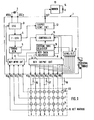
- Referring to Fig. 1, a remote control signal transmitter according to a first embodiment of the present invention generates a custom code and a key data_code representative of information of an operated key and outputs them as infrared rays by means of an
infrared ray diode 14. The custom code and key data code are produced by aremote control IC 1 from its output terminal OUT and then supplied to adrier circuit 13 to drive thediode 14. There is provided akey matrix 15 which is used to command the change in operation of an instrument to be remote-controlled. Thekey matrix 15 includes four row lines a to d, eight column lines e to l, and thirty-two key switches KS disposed at the respective intersections of the row and column lines. The row lines a to d are connected to key input terminals KI0 to KI3 of theIC 1, respectively, and the column lines e to 1 are connected to key output terminals KO0 to K07 of theIC 1, respectively. In order to setting a custom code designing the instrument to be.controlled, the selected key output terminals (in this embodiment, the first, fourth and eighth key output terminals KO0, K03 and K07) are connected to a power voltage source (not shown) viaresistors IC 1. The IC 1 has another power terminaly VSS which is in turn connected to a ground. - In a standby condition, all the key output terminals KO0 to KO7 of the
IC 1 assume a high level. When one of the key switches KS is operated or depressed to change the circuit operation of the remote-controlled instrument, any one of the key input terminals KI0 to KI3 is thereby supplied with the high level. This high level is detected by akey input circuit 6, and thecircuit 6 then supplies an oscillation-enable signal to anoscillator 3. Theoscillator 3 thus oscillates at a frequency determined by aresonant element 2 such as a crystal or a ceramic resonator connected between terminals OSC1 and OSC2. The oscillation signal of theoscillator 3 is frequency-divided by a divider 4 to a predetermined frequency signal, and in response to this predetermined frequency signal atiming generator 5 supplies timing signals to thekey input circuit 6, akey output circuit 7 and acontroller 11. Thekey output circuit 7 responds to the timing signal from thetiming generator 5 and a control signal from thecontroller 11 and outputs cyclically to the key output terminals KO to KO7 key scan signals used for detecting the operated key switch, but before this scan signal output operation, a custom code read operation is attained for reading-out the custom code alotted to the instrument to be controlled by this signal transmitter. - For this custom code read operation, a
level detection circuit 8 is provide to detect the level at each key output terminal KO. The input stage of thelevel detection circuit 8 as shown in Fig.'2, includes an N-channel MOS transistor Q3 connected between each key output terminal and the ground and supplied at.its.gate with a clock signal φ3 and P-channel and N-channel MOS transistors Q4 and Q5 constituting aninverter 30 which receives the level at each key output terminal KO. An output stage of thekey output circuit 7 is also shown in Fig. 2 and includes a P-channel MOS transistor Qi connected between the power terminal VDD and each key output terminal KO and supplied at its gate with a clock signal φ1 and an N-channel MOS transistor Q2 connected between each key output terminal KO and the ground and supplied at its gate with a clock signal φ2. In Fig. 2, the first key output terminal KO is represented, and therefore this terminal is connected to the power VDD via theresistor 16. - In Fig. 3, input stage of the
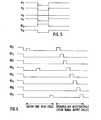
key input circuit 6 is shown. Each of the key input terminals KO0 to KI3 is connected to the ground via a pull-down resistor 19 and an N-channel MOS transistor Q8 receiving at its gate a clock signal φ4, and further connected to the gates of P-channel and N-channel MOS transistors Q6 and Q7. These transistors Q6 and Q7 are connected in series between the power terminals to constitute aninverter 31. - The custom code read operation will be described below with reference to a timing chart.shown in Fig. 4. In the standby condition, both of the clock signals φ1 and φ2 assume a low level, and hence all the key output terminals KO0 to KO7 take the high level. The
oscillator 3 starts to oscillate by the operation of one of the key switches KS, and in response to this, the clock signals φ1 and φ2 rise to the high level. As a result, the transistors Q1 and Q2 are turned OFF and ON, respectively. Since the conducting resistance of the transistor Q2 is selected to be sufficiently smaller than theresistors 16 to 18, all the key output terminals KO0 to K07 drops to the low level. In this state, the clock signal φ2 supplied to the transistor Q2 which is provided for the first key output terminal KO0, is inverted into the low level as shown in Fig. 4. The gates of transistors Q2 provided.for.the remaining key output terminals KO1 to KO7 are maintained at the high level. The clock signal φ3 is inverted into the low level in synchronism with the invertion of the clock φ2. The inversion of the clock signal φ3 occurs only for the first key output terminal KO0 and does not occur for the remaining key output terminals KO1 to KO7. The transistor Q3 connected to the first key output terminal KO0 is thus turned ON, so that the resistance-divided voltage appears at the first key output terminal KO0, which is represented by areference numeral 20 in Fig. 4 and determined by the conducting resistance of the transistor Q3 and theresistor 16. At this time, if the operated key KS is disposed on the first column line e, the impedance between the first key output terminal KO0 and the ground would be lowered due to the pull-down resistor 19, so that the above-mentioned resistance-divided voltage become close to the low level. Theresistor 16 does not achieve its function. In order to solve this defect, the clock signal φ4 takesthe low level in synchronium with the inversion of the clock signal ø2, so that the transistors Q8 provided for all the key input terminals KI0 to KI4 are turned OFF. The pull-down resistor 19 is thereby disconnected from the ground. The resistance-divided voltage at the key output terminal KO9. is determined by theresistor 16 and the conducting resistance of the transistor Q3. - The conducting resistance of the transistor Q3 is designed such that the resistance-divided voltage becomes larger than the logical threshold voltage of.the
inverter 30. Accordingly, the output voltage V30 of theinverter 30 takes the low level as shown in Fig. 4. As a result, the level detection circuit detects that the first key output terminal KO0 is connected to the power terminal VDD via theresistor 16 and supplies to a custom code register 10 a data "1", for example. - The clock signals φ2, φ3 and φ4 thereafter invert to the high level, the low level and the high level, respectively, so that the first key output terminal KO0 and the output voltage V30 of the
inverter 30 takes the low level and the high level, respectively. - Next, the clock signal φ2 supplied.to the transistor Q2 provided for the second key output terminal KO1 is inverted to the low level. In synchronism with this, the clock signals φ3 and φ4 are changed to.the high level and the low level, respectively. There is no resistor between the second key output terminal KO1 and the power terminal VDD. Therefore, the second key output terminal KO1 is held at the low level, and the output voltage V30 of the
inverter 30 is maintained at the high level. Thelevel detection circuit 8 thereby supplies a data "0" to thecustom code resistor 10. - The above-mention operation is continued for the remaining key output terminals KO2 to KO7. As a result, the voltage exceeding the threshold.voltage of the
inverter 30 appears at the first, fourth and eighth key output terminals KOO, KO3 and KO7 due to theresistors 16 to 18, as represented as a custom code read cycle in Fig. 6. Thelevel detection circuit 8 detects the level at each key output terminal and supplies to"theregister 10 the data corresponding to the detected level. Theregistor 10 thus stores data "10010001" therein at a time when the custom code read cycle is completed. The data stored in theregister 10 is used as a custom code. Various custom codes can be set by changing the key output terminal KO connected to the power terminal. VDD and/or by increasing or decreasing its number. In this embodiment, eight key output terminals are provided, and therefore 28 (= 256) kinds of custom codes can be set with the same typeremote control IC 1. - When the custom code read cycle ends, the
IC 1 is brought into an operated key switch detection cycle, i.e. a key scan signal output cycle. In this cycle, the clock signals φ1 and φ2 both takes the low level to turn the transistors Q1 and Q2 ON and OFF, respectively, as shown in Fig. 5. The first key output terminal KO0 is thereby .raised to the high level. The remaining key output terminals KO to KO7 are held at the low level. In the operated key detection cycle,.the clock signal φ3 assumes the low level to maintain the transistor Q3 in the nonconducting state. The clock signals φ4 is inverted into the low level in synchronism with the clock signals φ1 and φ2 to disconnect the pull-down resistor 19 in thekey input circuit 6 from the ground. The clock signal φ4 may be held at the high level, but in that case the . conducting resistance of the transistor Q1 is required to be sufficiently smaller than theresistor 19.. If the operated key switch is one of the key switches KS disposed on the first column line e, one of the key input terminals KI0 to KI3 is supplied with the high level. The input terminal KI supplied with the high level depends on the operated key. As a result, the inverter 31.produces its output voltage V31 having the low level. On the other hand, when the operated key is different.from any one of the key switches KS disposed on the column line e, the output voltage V31 of theinverter 31 does not change. - The clock signals φ1 and φ2 thereafter return to the high level, so that the first key output terminal KO is inverted to the low level.
- Similar operation is carried out with respect to the remaining key output terminals KO1 to KO7. As a result, pulse signals are outputted from the key output terminals KO0 to KO7 in that order, as shownas an operated key detection cycle in Fig. 6. That is, the scan signals are outputted. The operated key is thereby detected. The
key output circuit 7 includes a counter (not shown) therein, and the content thereof changes by.the fact that which key output terminal KO outputs the key scan signal. Although not shown, thekey input circuit 6 also includes a counter therein, and its count value varies by the fact that which key input terminal is supplied with the high level signal. The contents of these counters in the key input andoutput circuits level detection circuit 8 is in the non-activated state; and therefore thecircuit 8 does not produce any its output signal. - Although not shown, it is,general that the custom code read operation and the operated key detection (the.scan signal output) operation are carried out twice and the custom codes and key data codes obtained in the respective cycles are then compared with each other in order to prevent an error custom code and an error key data code. Moreover, it is also general to provide a multi-push cancellation circuit in order'to prevent the simultaneous pushing of two or more key switches, but such a construction is not related directly to the present invention and thus .is omitted.
- The custom code and key data code stored respectively in the
register controller 11. Thecontroller 11 performs the well-know Pulse-Position-Modulation (PPM) with respect to the read-out codes, and. further produces the inverted codes of the custom and key data codes. The inverted codes are also subjected to the PPM. The modulated non-inverted custom code, inverted custom code, non-inverted key data code and inverted key data code are supplied in that order to anoutput control circuit 12. Thecircuit 12 is also supplied with a signal of 38 KHz which is derived from the divider 4, and this signal is superposed on the respective codes as a carrier wave. The output of theoutput control circuit 12 is supplied to the-output terminal OUT of theIC 1 and further introduced into thedrive circuit 13. Thecircuit 13 controls the..ON and OFF states of theinfrared ray diode 14 in response to the signal from the output terminal oum. As a result, the custom code and the key data code are transmitted by means of infrared rays. - The instrument to be remote-controlled receives the command signal transmitted via the infrared rays and detects at first the custom code. The custom code.thus detected is then compared with that allotted to the instrument. When coinciding with each other, the instrument introduces the key data code and then performs the corresponding operation.
- As described above, the custom code for designing the instrument to be controlled is set without providing the custom code setting terminal, and further its kinds are changeable. Moreover, the
resistors 16 to 18 are used for setting the custom code, and diodes which are relatively expensive, are not recessary. - In the followings, other embodiments of the present invention will be described, and in the respective embodiments, the same constituents as those shown in Fig. 1 are indicated the same numerals to omit their further explanation. In addition, the circuit operations except for the custom code read operation are the same as the first embodiment.unless particular description is made, and therefore their explanations are omitted.
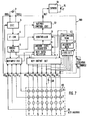
- Fig. 7 shows a second embodiment of the present invention. In this embodiment, a custom code ROM (Read-Only-Memory) 43 memorizing eight kinds of custom codes is provided in a remote-
control IC 100, and one of them is selected by connecting either one of eight key output terminals KO0 to K07 to the power terminal VDD via aresistor 40. Theresistor 40 is connected in this embodiment between the fifth key output terminal and the power terminal VDD. Accordingly, as has been mentioned with reference to Figs. 2 and 4, when the transistors Q2 and Q3 provided for the fifth key output terminal K04 are turned OFF and ON, respectively, the voltage exceeding the threshold level of theinverter 30 appears at that terminal KO4. Thelevel detection circuit 8 thereby produces data "1", for example. Before this and after this, thecircuit 8 produces data "0". The output data of thecircuit 8 are supplied'to anaddress generator 42. Thegenerator 42 generates an address signal responsive to the output of thecircuit 8 and then supplied it to thecustom code ROM 43. As a result, the custom code stored in the fifth address of theROM 43 is read-out and then supplied to thecustom code register 10, - The address varies by changing the key output terminal KO coupled to the power terminal VDD, and the custom code stored in the
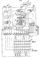
register 10 is thereby changed. Also in this embodiment, the custom code setting terminal is not required. If a plurality of key output terminals are coupled to the power terminal VDD, many kinds of address signals more than eight are generated. In accordance this, the memory capacity of the ROM can be increase to set a larger number of custom codes. - Fig. 8 shows the third embodiment of the present invention. In this embodiment, as indicating a remote-control IC by 200, a custom code setting terminal (CCS terminal) is provided on the
IC 200. A selected first group of the key output terminals (KOO, K04 and KO7 in this embodiment) is coupled to the power terminal VDD viaresistors diodes level detection circuit 8 but also that employing the CCS terminal are provided to produce an extremely large number of custom codes. - For the purposes of both custom code setting functions, the output stage of the
key output circuit 7 and the input stage of thekey detection circuit 8 have the same circuit constructions as those of Fig. 2, but the clock signals φ1 to φ3 supplied to the respective transistors are different from those of Fig. 4, as shown in Fig. 9. More particularly, when theoscillator 3 starts to oscillate, all the key output terminals KOO to K07 take the low level, followed by the inversions of the clock signal φ1 and φ2 supplied to the transistors Q1 and Q2 provided for the first key output terminals KOO. The transistors Q1 and Q2 are thereby turned ON and OFF, respectively, the first key output terminal KO0 is changed to the high level. At this time, the clock signal φ3 is in the low level. In this embodiment, since the first key output terminal KO0 is connected to the CCS terminal via thediode 44, the terminal CCS is supplied with the high level. Thekey input circuit 6 is coupled to the CCS terminal and detects the high level at that terminal to produce data "1", for example. This data is supplied to a first custom code register 10-1. If the diode 4.4 is not provided, the CCS terminal is in the low level, and therefore the register 10-1 receives data "0". Theinverter 30 connected to the first key output terminal KO0 produces the low level as its output voltage V30, but thelevel detection circuit 8 rejects the output voltage V30 by a control signal from thecontroller 11. As a result, it is detected whether or not the first key output terminal KO0 is connected to the CCS terminal via a diode. In other words, the diode read operation is carried out when all of the clock signals φ1, φ2 and φ3 are in the low level, as shown in Fig. 9. - In order to detect whether or not the first key output terminal KO0 is connected to the power terminal VDD via a resistor, the clock signals φ1 and φ3 are both inverted into the high level to turn the transistor Q1 and Q3 OFF and ON, respectively. In this embodiment, the first key output terminal KOO is connected via the resistor 41 to the power terminal VDD. Therefore, the resistance-divided voltage determined by the resistor 41 and the conducting resistance of the transistor Q3 appears at the first key output terminal KO0, Since this divided voltage exceeds the threshold voltage of the
inverter 30, the output voltage.V30 is held at the low level as shown in Fig. 9. Thelevel datection circuit 8 takes up the output voltage V30 at this time and supplies data "1" to a second custom code register 10-2. The divided voltage appearing at the terminal KO0 does not make the diode 44'conductive, and hence the CCS terminal assumes the low level. The divided voltage may turn thediode 44 ON, and in that case, thekey input circuit 6 is required to be in the non-activated state by another control signal from thecontroller 11. As a result, a resistor read-out operation is carried out. - The diode read-out operation and the.resistor read-out operation are then attained with respect to the second key output terminal KO1. This terminal KO1 is connected to the CCS terminal via the
diode 45, but no resistor is inserted between the terminals KO1 and VDD. Therefore, data "1" is stored into the first custom code register 10-1, and data "0" is stored in the'second custom code register 10-2. - Thereafter, the above-mentioned operations are carried out to the eighth key output terminal KO7, so that a timing chart represented as a custom code read operation in Fig. 10 is obtained. Since the
diodes resistors - The operated key detection operation is thereafter carried out in a.similar manner to that described with reference to the first embodiment, followed by the output of the custom and key data codes.
- With respect to the custom code output, the following three methods can be employed. In the first method, the data stored in the first and second custom code register 10-1 and 10-2 are outputted without any modification. That is, as shown in Fig. 11A, in the custom code composed of sixteen bits, a custom code (1) composed of Ci-bit to C8-bit is constructed by the data "11100100" of the first register 10-1, and a.custom code (2) composed of C1'-bit to C8'-bit is constructed by the data "10001001" of the second register 10-2. After the output of the custom code, a key code data composed of K1-bit to K8-bit and its inverted key code data (K̅1-bit to K̅8-bit) are outputtted. In addition, before the output of the codes, a transmission- enable signal called as a leader pulse is generated.
- The second custom code output method is shown in Fig. 11B. The data "11100100" stored in the first register 10-1 is used as the custom code (1) composed of Cl-bit to C8-bit. On the other hand, not only the data stored in the second register 10-2 but also that in the first register 10-1 are utilized as the customer code (2) composed of C1'-bit to C8'-bit. The custom code (2) is obtained by inverting the data stored in the bits in the first register 10-1 except for the bits corresponding to those in the second register 10-2 storing the data "1". Since the bits C1', C5' and C8' stores the data "1" in the second register 10-2 , the data stored in the bits C 1, C5 and C8 in the first register 10-1 are not inverted and the data stored in the remaining bits are inverted. As a result, the custom code (2) takes data "10010010".
- The third custom code output method is such that a custom code ROM 48 represented by a dotted line in Fig. 8 is provided in
IC 200 and the data stored in the ROM 48 is utilized along with the data stored in the registers 10-1 and 10-2. The custom code ROM 48 is a sixteen bits construction and stores data "0001000101100000". Thecontroller 11 reads out the data stored in the registers 10-1 and 10-2 as well as the data stored in the ROM 48, and obtains a first logical ORed data of the first half eight-bits data of the ROM 48 and the data of the register 10-1 and a second logical ORed data of the Second half eight-bits data of the ROM 48 and the data of the register 10-2. The first and second logical ORed data are "11110101" and "11101001", respectively, in consequence. Thecontroller 11 outputs the first logical ORed data as the custom code (1). On the other hand, the custom code (2) is obtained by inverting.the data stored in the bits in the first logical ORed data except for the bits corresponding to those in the second logical ORed data storing the data "I". Accordingly, the custom codes (1) and (2) assume the data "11110101" and "11100011", respectively. - Thus, various method can be employed to output the custom code, and in every custom code output method, the number of a presettable custom codes is 216 = 65536. In other words, the signal transmitter according to this embodiment provides an extremely large kinds of custom codes by employing a remote-control IC haying the same terminal number as the prior art.
- The data stored in the second register 10-2 may be used as a custom code (1).
- Fig. 12 shows a fourth embodiment of the present invention. Also in this embodiment, the custom code setting function usirig the CCS terminal and that using the
level detection circuit 8 are provided similarly to the third embodiment, but the custom code setting function using the CCS terminal is different in its construction from that of the third embodiment. The CCS terminal is connected to only one of the first to eighth key output terminals KO0 to KO7. (in this embodiment, the fourth key output terminal KO3). The custom code read operation is carried out similarly to the third embodiment. The second, fifth and sixth key output terminals KO1,KO4 and KO5 are connected to the power terminal VDD viaresistors address generator 51 coupled to the CCS terminal generates an address signal that selects the fourth address of acustom code ROM 50. TheROM 50 memorizes eight kinds of custom codes. The data read-out from theROM 50 is supplied to the first register 10-1. - As described above, one of eight kinds of custom codes is selected by connecting only one of the key output terminals KO to the CCS terminal, and a greater number of custom codesare further produced by the
resistors 52 to 54. - A fifth embodiment of the present invention is shown in Fig. 13. In this embodiment, the
detection circuit 8 detects the level at the seventh and eighth key output terminals XO6 and KO7. The output of thecircuit 8 is supplied to anaddress generator 61, and one address of. acustom code ROM 62 is thereby selected. TheROM 62 stores four kinds of custom codes therein. Each of custom codes is a five-bits construction. Although aresistor 64 is inserted between the eighth key output terminal KO7 and the power terminal VDD' the relationship between the presence/absence of a resistor connected to the terminals K06 and KO7 and the address number of theROM 62 is represented by the following Table-1:
ROM 62 is supplied to acustom code register 63 and stored in its latter five-bits. - On the other hand, the CCS terminal is connected either one of the first to eighth key output terminals KO0 to KO7, and in response to the connecting location, a
code generation circuit 60 generates data camposed of three-bits and represented by the following Table-2;
generator 60 is supplied to theregister 63 and stored in its former three-bits. - As a result, the
custom code register 63 storing a custom code of an eight-bits construction. Thecontroller 11 thereafter processes the signal, as has been already mentioned. - The present invention is not limited to the aforementioned embodiments, but can be modified and changed without departing from the scope and spirit of the invention. For example, the selected key output terminal or terminals may be connected to the ground potention, and in that case all the logic level mentioned above are inverted. It is also possible to connect the selected key output terminal directly to the potential source. In this case, the conducting resistance of the transistor Q3 is preferrably made large in order to reduce a power consumption.
Claims (9)
Applications Claiming Priority (2)
| Application Number | Priority Date | Filing Date | Title |
|---|---|---|---|
| JP20433/85 | 1985-02-05 | ||
| JP2043385 | 1985-02-05 |
Publications (3)
| Publication Number | Publication Date |
|---|---|
| EP0190743A2 true EP0190743A2 (en) | 1986-08-13 |
| EP0190743A3 EP0190743A3 (en) | 1988-08-31 |
| EP0190743B1 EP0190743B1 (en) | 1992-12-30 |
Family
ID=12026907
Family Applications (1)
| Application Number | Title | Priority Date | Filing Date |
|---|---|---|---|
| EP86101476A Expired EP0190743B1 (en) | 1985-02-05 | 1986-02-05 | Control signal generation circuit for wireless remote control signal transmitter |
Country Status (4)
| Country | Link |
|---|---|
| US (1) | US5059975A (en) |
| EP (1) | EP0190743B1 (en) |
| JP (1) | JPS625798A (en) |
| DE (1) | DE3687353T2 (en) |
Cited By (1)
| Publication number | Priority date | Publication date | Assignee | Title |
|---|---|---|---|---|
| EP0217283A2 (en) * | 1985-09-30 | 1987-04-08 | Kabushiki Kaisha Toshiba | Key circuit |
Families Citing this family (6)
| Publication number | Priority date | Publication date | Assignee | Title |
|---|---|---|---|---|
| US5254989A (en) * | 1988-12-20 | 1993-10-19 | Bull S.A. | Garbling the identification of a key of a non-coded keyboard, and circuit for performing the method |
| KR100218009B1 (en) * | 1997-05-27 | 1999-09-01 | 윤종용 | Device and method for preventing key error by chattering noise |
| JP4908014B2 (en) * | 2006-02-27 | 2012-04-04 | 株式会社東芝 | Light emitting device and floor display system |
| CN102075194B (en) * | 2009-11-23 | 2015-03-11 | 鸿富锦精密工业(深圳)有限公司 | Circuit and method for scanning keyboard and electronic equipment |
| TWI439062B (en) * | 2010-07-02 | 2014-05-21 | Generalplus Technology Inc | Custom code setting system of a remote control chip |
| CA2909441A1 (en) | 2013-03-14 | 2014-09-25 | Soundwall Llc | Decorative flat panel sound system |
Citations (1)
| Publication number | Priority date | Publication date | Assignee | Title |
|---|---|---|---|---|
| US4412218A (en) * | 1980-02-26 | 1983-10-25 | Nippon Electric Co., Ltd. | Remote control signal transmitter capable of setting custom codes individually alloted to a plurality of controlled instruments |
Family Cites Families (1)
| Publication number | Priority date | Publication date | Assignee | Title |
|---|---|---|---|---|
| JPS53120158A (en) * | 1977-03-29 | 1978-10-20 | Sharp Corp | Power source control system |
-
1986
- 1986-02-05 DE DE8686101476T patent/DE3687353T2/en not_active Expired - Lifetime
- 1986-02-05 EP EP86101476A patent/EP0190743B1/en not_active Expired
- 1986-02-05 JP JP61024401A patent/JPS625798A/en active Granted
-
1988
- 1988-04-19 US US07/185,248 patent/US5059975A/en not_active Expired - Lifetime
Patent Citations (1)
| Publication number | Priority date | Publication date | Assignee | Title |
|---|---|---|---|---|
| US4412218A (en) * | 1980-02-26 | 1983-10-25 | Nippon Electric Co., Ltd. | Remote control signal transmitter capable of setting custom codes individually alloted to a plurality of controlled instruments |
Cited By (2)
| Publication number | Priority date | Publication date | Assignee | Title |
|---|---|---|---|---|
| EP0217283A2 (en) * | 1985-09-30 | 1987-04-08 | Kabushiki Kaisha Toshiba | Key circuit |
| EP0217283A3 (en) * | 1985-09-30 | 1988-10-05 | Kabushiki Kaisha Toshiba | Key circuit |
Also Published As
| Publication number | Publication date |
|---|---|
| JPS625798A (en) | 1987-01-12 |
| EP0190743B1 (en) | 1992-12-30 |
| EP0190743A3 (en) | 1988-08-31 |
| JPH0481396B2 (en) | 1992-12-22 |
| DE3687353T2 (en) | 1993-05-27 |
| DE3687353D1 (en) | 1993-02-11 |
| US5059975A (en) | 1991-10-22 |
Similar Documents
| Publication | Publication Date | Title |
|---|---|---|
| US4482947A (en) | Multi-function, multi-unit remote control system and method therefor | |
| US4412218A (en) | Remote control signal transmitter capable of setting custom codes individually alloted to a plurality of controlled instruments | |
| EP0492482B1 (en) | Non contact type IC-card | |
| US4115706A (en) | Integrated circuit having one-input terminal with selectively varying input levels | |
| US5059975A (en) | Control signal generation circuit for wireless remote control signal transmitter | |
| US4118791A (en) | Multi-level encoding system | |
| US4376995A (en) | Timekeeping device | |
| US5231389A (en) | Display control for selecting oscillating signals | |
| US5969648A (en) | Quaternary signal encoding | |
| JPH0944467A (en) | Microcomputer | |
| US4291221A (en) | Digital semiconductor circuit | |
| US6828829B2 (en) | Semiconductor device having input buffers to which internally-generated reference voltages are applied | |
| JPH0548016A (en) | Semiconductor integrated circuit device | |
| JPH06194417A (en) | Generating circuit of clock signal | |
| KR100228562B1 (en) | Remote controller | |
| JPH0727833A (en) | Test signal producing device | |
| KR100418520B1 (en) | Code selector of programmable impedance output driver | |
| JPS6140353B2 (en) | ||
| JP2557703B2 (en) | Mode setting circuit | |
| JPS6222433B2 (en) | ||
| US3947773A (en) | Channel number memory for television tuners | |
| KR960002930B1 (en) | The same state switching of input/output | |
| JPH11296400A (en) | Mode setting circuit | |
| KR950000425B1 (en) | Serial input/output memory with high speed test device | |
| KR19990072694A (en) | Device with a clock output circuit |
Legal Events
| Date | Code | Title | Description |
|---|---|---|---|
| PUAI | Public reference made under article 153(3) epc to a published international application that has entered the european phase |
Free format text: ORIGINAL CODE: 0009012 |
|
| 17P | Request for examination filed |
Effective date: 19860205 |
|
| AK | Designated contracting states |
Kind code of ref document: A2 Designated state(s): DE FR GB |
|
| PUAL | Search report despatched |
Free format text: ORIGINAL CODE: 0009013 |
|
| AK | Designated contracting states |
Kind code of ref document: A3 Designated state(s): DE FR GB |
|
| 17Q | First examination report despatched |
Effective date: 19901018 |
|
| GRAA | (expected) grant |
Free format text: ORIGINAL CODE: 0009210 |
|
| AK | Designated contracting states |
Kind code of ref document: B1 Designated state(s): DE FR GB |
|
| ET | Fr: translation filed | ||
| REF | Corresponds to: |
Ref document number: 3687353 Country of ref document: DE Date of ref document: 19930211 |
|
| PLBE | No opposition filed within time limit |
Free format text: ORIGINAL CODE: 0009261 |
|
| STAA | Information on the status of an ep patent application or granted ep patent |
Free format text: STATUS: NO OPPOSITION FILED WITHIN TIME LIMIT |
|
| 26N | No opposition filed | ||
| REG | Reference to a national code |
Ref country code: GB Ref legal event code: IF02 |
|
| REG | Reference to a national code |
Ref country code: GB Ref legal event code: 732E |
|
| REG | Reference to a national code |
Ref country code: FR Ref legal event code: TP |
|
| PGFP | Annual fee paid to national office [announced via postgrant information from national office to epo] |
Ref country code: GB Payment date: 20050202 Year of fee payment: 20 |
|
| PGFP | Annual fee paid to national office [announced via postgrant information from national office to epo] |
Ref country code: DE Payment date: 20050203 Year of fee payment: 20 |
|
| PGFP | Annual fee paid to national office [announced via postgrant information from national office to epo] |
Ref country code: FR Payment date: 20050208 Year of fee payment: 20 |
|
| PG25 | Lapsed in a contracting state [announced via postgrant information from national office to epo] |
Ref country code: GB Free format text: LAPSE BECAUSE OF EXPIRATION OF PROTECTION Effective date: 20060204 |
|
| REG | Reference to a national code |
Ref country code: GB Ref legal event code: PE20 |