EP0189309A2 - Halbleiteranordnung und Verfahren ihrer Herstellung mittels Molekularstrahl-Epitaxie - Google Patents
Halbleiteranordnung und Verfahren ihrer Herstellung mittels Molekularstrahl-Epitaxie Download PDFInfo
- Publication number
- EP0189309A2 EP0189309A2 EP86300388A EP86300388A EP0189309A2 EP 0189309 A2 EP0189309 A2 EP 0189309A2 EP 86300388 A EP86300388 A EP 86300388A EP 86300388 A EP86300388 A EP 86300388A EP 0189309 A2 EP0189309 A2 EP 0189309A2
- Authority
- EP
- European Patent Office
- Prior art keywords
- single crystalline
- mgo
- semiconductor device
- silicon substrate
- film
- Prior art date
- Legal status (The legal status is an assumption and is not a legal conclusion. Google has not performed a legal analysis and makes no representation as to the accuracy of the status listed.)
- Granted
Links
Images



Classifications
-
- H—ELECTRICITY
- H10—SEMICONDUCTOR DEVICES; ELECTRIC SOLID-STATE DEVICES NOT OTHERWISE PROVIDED FOR
- H10P—GENERIC PROCESSES OR APPARATUS FOR THE MANUFACTURE OR TREATMENT OF DEVICES COVERED BY CLASS H10
- H10P14/00—Formation of materials, e.g. in the shape of layers or pillars
- H10P14/60—Formation of materials, e.g. in the shape of layers or pillars of insulating materials
- H10P14/69—Inorganic materials
- H10P14/692—Inorganic materials composed of oxides, glassy oxides or oxide-based glasses
- H10P14/6938—Inorganic materials composed of oxides, glassy oxides or oxide-based glasses the material containing at least one metal element, e.g. metal oxides, metal oxynitrides or metal oxycarbides
- H10P14/6939—Inorganic materials composed of oxides, glassy oxides or oxide-based glasses the material containing at least one metal element, e.g. metal oxides, metal oxynitrides or metal oxycarbides characterised by the metal
-
- H—ELECTRICITY
- H10—SEMICONDUCTOR DEVICES; ELECTRIC SOLID-STATE DEVICES NOT OTHERWISE PROVIDED FOR
- H10P—GENERIC PROCESSES OR APPARATUS FOR THE MANUFACTURE OR TREATMENT OF DEVICES COVERED BY CLASS H10
- H10P14/00—Formation of materials, e.g. in the shape of layers or pillars
- H10P14/20—Formation of materials, e.g. in the shape of layers or pillars of semiconductor materials
- H10P14/22—Formation of materials, e.g. in the shape of layers or pillars of semiconductor materials using physical deposition, e.g. vacuum deposition or sputtering
-
- H—ELECTRICITY
- H10—SEMICONDUCTOR DEVICES; ELECTRIC SOLID-STATE DEVICES NOT OTHERWISE PROVIDED FOR
- H10P—GENERIC PROCESSES OR APPARATUS FOR THE MANUFACTURE OR TREATMENT OF DEVICES COVERED BY CLASS H10
- H10P14/00—Formation of materials, e.g. in the shape of layers or pillars
- H10P14/20—Formation of materials, e.g. in the shape of layers or pillars of semiconductor materials
- H10P14/29—Formation of materials, e.g. in the shape of layers or pillars of semiconductor materials characterised by the substrates
- H10P14/2901—Materials
- H10P14/2902—Materials being Group IVA materials
- H10P14/2905—Silicon, silicon germanium or germanium
-
- H—ELECTRICITY
- H10—SEMICONDUCTOR DEVICES; ELECTRIC SOLID-STATE DEVICES NOT OTHERWISE PROVIDED FOR
- H10P—GENERIC PROCESSES OR APPARATUS FOR THE MANUFACTURE OR TREATMENT OF DEVICES COVERED BY CLASS H10
- H10P14/00—Formation of materials, e.g. in the shape of layers or pillars
- H10P14/20—Formation of materials, e.g. in the shape of layers or pillars of semiconductor materials
- H10P14/32—Formation of materials, e.g. in the shape of layers or pillars of semiconductor materials characterised by intermediate layers between substrates and deposited layers
- H10P14/3202—Materials thereof
- H10P14/3204—Materials thereof being Group IVA semiconducting materials
- H10P14/3211—Silicon, silicon germanium or germanium
-
- H—ELECTRICITY
- H10—SEMICONDUCTOR DEVICES; ELECTRIC SOLID-STATE DEVICES NOT OTHERWISE PROVIDED FOR
- H10P—GENERIC PROCESSES OR APPARATUS FOR THE MANUFACTURE OR TREATMENT OF DEVICES COVERED BY CLASS H10
- H10P14/00—Formation of materials, e.g. in the shape of layers or pillars
- H10P14/20—Formation of materials, e.g. in the shape of layers or pillars of semiconductor materials
- H10P14/32—Formation of materials, e.g. in the shape of layers or pillars of semiconductor materials characterised by intermediate layers between substrates and deposited layers
- H10P14/3202—Materials thereof
- H10P14/3238—Materials thereof being insulating materials
-
- H—ELECTRICITY
- H10—SEMICONDUCTOR DEVICES; ELECTRIC SOLID-STATE DEVICES NOT OTHERWISE PROVIDED FOR
- H10P—GENERIC PROCESSES OR APPARATUS FOR THE MANUFACTURE OR TREATMENT OF DEVICES COVERED BY CLASS H10
- H10P14/00—Formation of materials, e.g. in the shape of layers or pillars
- H10P14/20—Formation of materials, e.g. in the shape of layers or pillars of semiconductor materials
- H10P14/32—Formation of materials, e.g. in the shape of layers or pillars of semiconductor materials characterised by intermediate layers between substrates and deposited layers
- H10P14/3242—Structure
- H10P14/3244—Layer structure
- H10P14/3251—Layer structure consisting of three or more layers
- H10P14/3252—Alternating layers, e.g. superlattice
-
- H—ELECTRICITY
- H10—SEMICONDUCTOR DEVICES; ELECTRIC SOLID-STATE DEVICES NOT OTHERWISE PROVIDED FOR
- H10P—GENERIC PROCESSES OR APPARATUS FOR THE MANUFACTURE OR TREATMENT OF DEVICES COVERED BY CLASS H10
- H10P14/00—Formation of materials, e.g. in the shape of layers or pillars
- H10P14/20—Formation of materials, e.g. in the shape of layers or pillars of semiconductor materials
- H10P14/34—Deposited materials, e.g. layers
- H10P14/3402—Deposited materials, e.g. layers characterised by the chemical composition
- H10P14/3404—Deposited materials, e.g. layers characterised by the chemical composition being Group IVA materials
- H10P14/3411—Silicon, silicon germanium or germanium
-
- H—ELECTRICITY
- H10—SEMICONDUCTOR DEVICES; ELECTRIC SOLID-STATE DEVICES NOT OTHERWISE PROVIDED FOR
- H10P—GENERIC PROCESSES OR APPARATUS FOR THE MANUFACTURE OR TREATMENT OF DEVICES COVERED BY CLASS H10
- H10P14/00—Formation of materials, e.g. in the shape of layers or pillars
- H10P14/60—Formation of materials, e.g. in the shape of layers or pillars of insulating materials
- H10P14/63—Formation of materials, e.g. in the shape of layers or pillars of insulating materials characterised by the formation processes
- H10P14/6326—Deposition processes
- H10P14/6328—Deposition from the gas or vapour phase
- H10P14/6334—Deposition from the gas or vapour phase using decomposition or reaction of gaseous or vapour phase compounds, i.e. chemical vapour deposition
-
- H—ELECTRICITY
- H10—SEMICONDUCTOR DEVICES; ELECTRIC SOLID-STATE DEVICES NOT OTHERWISE PROVIDED FOR
- H10P—GENERIC PROCESSES OR APPARATUS FOR THE MANUFACTURE OR TREATMENT OF DEVICES COVERED BY CLASS H10
- H10P14/00—Formation of materials, e.g. in the shape of layers or pillars
- H10P14/60—Formation of materials, e.g. in the shape of layers or pillars of insulating materials
- H10P14/63—Formation of materials, e.g. in the shape of layers or pillars of insulating materials characterised by the formation processes
- H10P14/6326—Deposition processes
- H10P14/6349—Deposition of epitaxial materials
-
- H—ELECTRICITY
- H10—SEMICONDUCTOR DEVICES; ELECTRIC SOLID-STATE DEVICES NOT OTHERWISE PROVIDED FOR
- H10P—GENERIC PROCESSES OR APPARATUS FOR THE MANUFACTURE OR TREATMENT OF DEVICES COVERED BY CLASS H10
- H10P14/00—Formation of materials, e.g. in the shape of layers or pillars
- H10P14/60—Formation of materials, e.g. in the shape of layers or pillars of insulating materials
- H10P14/69—Inorganic materials
- H10P14/692—Inorganic materials composed of oxides, glassy oxides or oxide-based glasses
- H10P14/6938—Inorganic materials composed of oxides, glassy oxides or oxide-based glasses the material containing at least one metal element, e.g. metal oxides, metal oxynitrides or metal oxycarbides
- H10P14/6939—Inorganic materials composed of oxides, glassy oxides or oxide-based glasses the material containing at least one metal element, e.g. metal oxides, metal oxynitrides or metal oxycarbides characterised by the metal
- H10P14/69391—Inorganic materials composed of oxides, glassy oxides or oxide-based glasses the material containing at least one metal element, e.g. metal oxides, metal oxynitrides or metal oxycarbides characterised by the metal the material containing aluminium, e.g. Al2O3
-
- H—ELECTRICITY
- H10—SEMICONDUCTOR DEVICES; ELECTRIC SOLID-STATE DEVICES NOT OTHERWISE PROVIDED FOR
- H10P—GENERIC PROCESSES OR APPARATUS FOR THE MANUFACTURE OR TREATMENT OF DEVICES COVERED BY CLASS H10
- H10P14/00—Formation of materials, e.g. in the shape of layers or pillars
- H10P14/60—Formation of materials, e.g. in the shape of layers or pillars of insulating materials
- H10P14/69—Inorganic materials
- H10P14/692—Inorganic materials composed of oxides, glassy oxides or oxide-based glasses
- H10P14/6938—Inorganic materials composed of oxides, glassy oxides or oxide-based glasses the material containing at least one metal element, e.g. metal oxides, metal oxynitrides or metal oxycarbides
- H10P14/6939—Inorganic materials composed of oxides, glassy oxides or oxide-based glasses the material containing at least one metal element, e.g. metal oxides, metal oxynitrides or metal oxycarbides characterised by the metal
- H10P14/69397—Inorganic materials composed of oxides, glassy oxides or oxide-based glasses the material containing at least one metal element, e.g. metal oxides, metal oxynitrides or metal oxycarbides characterised by the metal the material containing two or more metal elements
Definitions
- the present invention relates to a semiconductor device and a method of producing same, in particular semiconductor device comprising a single crystalline silicon substrate provided with single crystalline films of oxides such as Al 2 O 3 , Mg0 and M g O.Al 2 0 3 laminated thereon and a method of producing same by Molecular Beam Epitaxy.
- Semiconductor device comprising a single crystalline silicon substrate provided with interlayer insulating films and silicon layers being alternatively laminated thereon and a circuit structure being incorporated therein have been developed.
- Metal oxides such as Al 2 O 3 , Mg0 and MgO ⁇ Al 2 O 3 have been used as the interlayer insulating films of such a semiconductor device, but these interlayer insulating films have been formed on the silicon substrate and each silicon layer usually by CVD (Chemical Vapor Deposition) in the form of single crystal, poly crystal or amorphous substance.
- MBE Molecular Beam Epitaxy
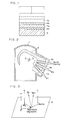
- FIG. 1 is a sectional view showing a construction of a semiconductor device according to the present invention
- interlayer insulating films 6a, 6b ... and silicon layers 7a, 7b ... are alternatively laminated on a single crystalline silicon substrate 5 to form a three dimensional circuit structure, that is to say, an interlayer insulating film 6a, which is an oxide film, is laminated on the single crystalline silicon substrate 5, a silicon layer 7a being laminated on the interlayer insulating film 6a, an interlayer insulating film 6b being laminated on the silicon layer 7a, a silicon layer 7b being laminated on the interlayer insulating film 6b ....
- interlayer insulating film 6a laminated on the single crystalline silicon substrate 5 and the interlayer insulating films 6b ... arranged thereover are formed in the form of single crystalline layer and also each of the silicon layers 7a, 7b ... are formed in the form of single crystalline layer in this preferred embodiment, these can be formed in the form of poly crystalline layer or amorphous layer by changing the film-forming condition, as described later.
- FIG. 2 is a schematic side sectional view of a MBE apparatus for carrying out a method of producing a semiconductor device according to the present invention
- FIG. 3 is a schematic drawing showing the reactions making progress when MgO ⁇ Al 2 O 3 (magnesia spinel) is deposited on a single crystalline silicon substrate 5.
- referring numeral 1 designates a ultra-high vacuum vessel and 2 designates a cryoshroud disposed in the ultra-high vacuum vessel 1 and filled with liquid nitrogen.
- a sample-heating plate 3 provided therein with a heater (not shown) is installed within a space surrounded by the cryoshroud 2 and the single crystalline silicon substrate 5 is fixedly mounted on the surface of the sample-heating plate 3, concretely its surface being opposite to effusing cells 4a, 4b, 4c which are described later.
- the effusing cells 4a, 4b, 4c aim at supplying molecules of A1, Mg, and Sb 2 0 3 respectively, and pass through the cryoshroud 2 so as to direct the front ends thereof toward the single crystalline silicon substrate 5 fixedly mounted on the sample-heating plate 3, respectively.
- Al is housed in the effusing cell 4a, Mg in the effusing cell 4b, and the group V oxides as an oxygen source, for example Sb 2 0 3 (also A S2 0 3 and the like can be used), in the effusing cell 4c.
- These effusing cells 4a, 4b, 4c are constructed so that upon heating at the appointed temperatures, molecules of substances housed therein may be directed from the front ends thereof toward the silicon substrate 5 at the appointed speeds.
- the silicon substrate 5 is heated at the appointed temperature.
- the reaction expressed by the following equation (1) makes progress thereby forming a single crystalline, poly crystalline or amorphous layer of Al 2 0 3 which is an insulating oxide film, and gradually making the layer grow:
- FIG. 3 shows the reaction process expressed by the above described equation (3).
- oxide films to be formed as the insulating films 6a, 6b ... are formed of the above described MgO ⁇ Al 2 O 3 (magnesia spinel), A1 2 0 3 , Mg0 or the like.
- crystal forms of the oxide films are cubic being identical with that of a single silicon crystal of the substrate, and the formers are similar to the latter in lattice constant thereby the oxide films are easy to epitaxially grow.
- Al 2 O 3 usually having a hexagonal crystal form, ⁇ -type one has a cubic crystal form in a stabilized range of 900°C or less, it can be used.
- fluorides such as CaF 2 and SrF 2 can be used, too.
- Sb203 is used as an oxygen source in the present invention
- the oxygen source is not limited to the use of Sh 2 0 3 .
- other group V oxides can be used.
- the reason why the group V oxides are preferably used as an oxygen source is that the group V elements, above all Sb, have a lower sticking coefficient thereby their linkage with oxygens is easy to cancel, and they are difficult to link with Si atoms constructing the silicon substrate 5.
- the reason why the group V oxides, above all an oxide of Sb (for example Sb203), are used as an oxygen source is that not only the vacuum condition within the ultra-high vacuum vessel 1 is hardly dropped but also impurities can be prevented from depositing to the silicon substrate 5.
- the especially important conditions for obtaining single crystalline oxide films are (1) the substrate temperature, (2) the ratio of atom numbers, (3) the film growth speed and the like. And, as far as these three conditions and other incidental conditions are satisfied, the oxide film, which can be deemed as an almost single crystalline layer, can be laminated on a single crystalline silicon substrate, even though a slight quantity of poly crystalline portion is contained in the single crystalline layer.
- the oxide film which can be deemed as an almost single crystalline layer, can be laminated on a single crystalline silicon substrate, even though a slight quantity of poly crystalline portion is contained in the single crystalline layer.
- a substrate temperature that is a temperature of a surface, on which an insulating oxide film 6a is formed, of a silicon substrate 5 is a certain extent of temperature or more
- molecules of an oxide film substance such as A1203
- the substrate temperature is a certain extent of temperature or less
- plenty of molecules are deposited thereby growing a poly crystalline layer.
- an amorphous layer is formed.
- the substrate temperature is a certain temperature, concretely about 900 o C, or less in order to protect the silicon substrate 5 and semiconductor elements formed on the silicon substrate 5.
- the substrate temperature of 750°C or more (but 900°C or less) is required in order to form an insulating single crystalline oxide film formed of Al 2 O 3 on a single crystalline silicon substrate.
- the substrate temperature is below 700°C, a poly crystalline layer is formed, and in case where the substrate temperature is further lower, an amorphous layer is formed.
- a single crystalline film is formed at the substrate temperature of 700°C or more (but 900°C or less), a poly crystalline film at temperatures below 700°C, and an amorphous film at further lower temperatures.
- a single crystalline film is formed at the substrate temperature of 800°C or more (but 900°C or less), a poly crystalline film at temperatures below 800°C, and an amorphous film at further lower temperatures.
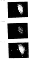
- RHEED (Reflection High Energy Electron Diffraction) patterns as shown in FIGS. 4-1 to 3 show the differences in crystallinity depending upon the above described substrate temperatures. Concretely speaking, this is a case where the crystals of MgO ⁇ Al 2 O 3 are grown on a single crystalline silicon substrate with Sb 2 0 3 as an oxygen source.
- a temperature of an Al cell (4a in FIG. 2) was held constant at 1,100°C, that of a Mg cell (4b in FIG. 2) constant at 350°C, and a pressure of As 2 O 3 constant at 2.5 x 10 -8 Torr.
- FIG. 4-1 shows the results of the growth of MgO ⁇ Al 2 O 3 in the case where a temperature of the single crystalline silicon substrate is held at 800°C. A streaked pattern proving a single crystalline structure was obtained.
- FIG. 4-2 shows the results of the same in the case where a temperature of the single crystalline silicon substrate is held at 700°C. A ringed pattern proving a poly crystalline structure was obtained.
- FIG. 4-3 shows the results of the same in case where a temperature of the substrate is held at 500°C. A hollow pattern proving an amorphous structure was obtained.
- RHEED patterns as shown in FIGS. 5-1 to 3 show the differences in crystallinity in case where the crystals of MgO ⁇ Al 2 O 3 are grown on a single crystalline silicon substrate with As 2 O 3 as an oxygen source. Excepting that a pressure of A S2 0 3 was 2.8 x 10 -8 Torr constant, the conditions were same as in case where Sb 2 0 3 was used as an oxygen source. Accordingly, at the substrate temperature 800°C a streaked pattern proving a single crystalline structure was obtained as shown in FIG. 5-1, at the substrate temperature 700°C a ringed pattern proving a poly crystalline structure as shown in FIG. 5-2, at the substrate temperature 500°C a hollow pattern proving an amorphous structure as shown in FIG. 5-3.
- a single crystalline layer is obtained at the substrate temperature of 900 C or less but over a certain temperature to protect a silicon substrate and semiconductor elements formed thereon.
- the ratios of a number of metal atoms, such as Al, Mg and Al + Mg, which construct molecules of the substances of oxide films, to an oxygen atom are preferably 2 to 4 regardless of the kinds of the substances of oxide films.
- An amorphous oxide film is formed in case where a ratio of a number of oxygen atoms to a number of metal atoms is less than 2, and one or some bonds of a metal atom are not linked with oxygen atoms, so that the formed oxide film becomes shortage of oxygen, thereby optical- and electronic characteristics are deteriorated.
- FIG. 6-1 to 3 show the relations between pressures of Sb 2 O 3 and the crystallinity of the formed oxide film of MgO ⁇ Al 2 O 3 grown on a single crystalline silicon substrate at the constant substrate temperature of 800°C with Sb 2 O 3 as an oxygen source.
- the temperatures of an Al cell and a Mg cell were held constant (1,100°C and 350°C). In other words, the number of Al atoms and Mg atoms supplied was held constant but the number of oxygen atoms supplied was varied.
- FIG. 6-1 shows a RHEED pattern of a MgO ⁇ Al 2 O 3 film formed in case where a pressure of Sb 2 0 3 is high to an extent of 1 x 10- 7 Torr, in other words a ratio of a number of oxygen atoms to a number of metal atoms is large. A ringed pattern proving a poly crystalline structure was obtained.
- FIG. 6-2 shows a RHEED pattern of a MgO ⁇ Al 2 O 3 film formed in case where a pressure of Sb 2 0 3 is 2.5 x 10 -8 Torr (the optimum condition), in other words a ratio of a number of oxygen atoms to a number of metal atoms is 2 to 4. A streaked pattern proving a single crystalline structure was obtained.
- FIG. 6-3 shows a RHEED pattern of a MgO ⁇ Al 2 O 3 film formed in case where a pressure of Sb 2 O 3 is low to an extent of 1.0 x 10 Torr, in other words a ratio of a number of oxygen atoms to a number of metal atoms is small. A hollow pattern proving an amorphous structure was obtained.
- FIGS. 7-1 to 3 show RHEED patterns of MgO ⁇ Al 2 O 3 grown on a single crystalline silicon substrate similarly to the above described with As 2 O 3 as an oxygen source.
- a substrate temperature was 800°C
- a temperature of an Al cell 1,100°C was 800°C
- a temperature of a Mg cell 350°C was obtained as FIG. 7-1 showing a RHEED pattern of a MgO ⁇ Al 2 O 3 film formed in case where a ratio of a number of oxygen atoms to a number of metal atoms is large and a pressure of As 2 O 3 is 1 x 10 -7 Torr.
- FIG. 7-2 showing a RHEED pattern of a MgO ⁇ Al 2 O 3 film formed in case where a ratio of a number of oxygen atoms to a number of metal atoms is 2 to 4 and a pressure of As 2 0 3 is 2.8 x 10 -8 Torr.
- FIG. 7-3 showing a RHEED pattern of a MgO.Al 2 0 3 film formed in case where a ratio of a number of oxygen atoms to a number of metal atoms is small and a pressure of A s 2 0 3 is 1.0 x 10 -8 Torr.
- a single crystalline oxide film of metals such as Al, Mg and Al + Mg can be formed on a single crystalline silicon substrate.
- Every oxide film of A1203, Mg0 and MgO ⁇ Al 2 O 3 was formed at a film-growth speed of 0.1 to 2.O ⁇ m/hour.
- the crystals are difficult to grow at a film-growth speed of 0.l ⁇ m/hour or less, and poly crystals are formed at a film-growth speed of 2.0 ⁇ m/hour or more.
- the reason of the above described is that new molecules deposit to a crystal before the crystal grows in the form of a single crystal, thereby forming a poly crystal in case where the film-growth speed exceeds 2.0 ⁇ m/hour.
- an Al cell temperature and a Mg cell temperature as shown in Table 1 determine a number of Al atoms and Mg atoms supplied from the effusing cells 4a, 4b, respectively.
- a pressure of Sb 2 0 3 as shown in Table 1 is determined by a temperature of the effusing cell 4c and determines a number of oxygen atoms to be supplied.
- a pressure of Sb 2 0 3 is set at 2.0 x 10 -8 , 2.0 x 10- 7 and 2.5 x 10⁻⁸ Torr for A1 2 0 3 , Mg0 and MgO ⁇ Al 2 O 3 , respectively, on the basis of a vacuum condition within a ultra-high vacuum vessel 1 and then a temperature of each of the effusing cells 4a, 4b and 4c is determined so that a ratio of a number of oxygen atoms to a number of metal atoms may be 2 to 4 in dependence upon the pressure of Sb 2 O 3 .
- a single crystalline oxide film such as Al 2 0 31 MgO or MgO ⁇ Al 2 O 3 , which are oxides of a metal such as Al, Mg or Mg + Al, on a single crystalline silicon substrate, a pressure of Sb 2 O 3 at 2.0 x 10 -8 , 2.0 x 10 -7 and 2.5 x 10 -8 Torr, respectively, a temperature of an Al cell at 1,100°C in either case of Al 2 0 3 or MgO ⁇ Al 2 O 3 , a temperature of a Mg cell at 550°C for Mg0 and 350°C for MgO ⁇ Al 2 O 3 , a ratio of a number of oxygen atoms to a number of metal atoms at 2 to 4, and a crystal-growth speed at 0.1 to
Landscapes
- Physical Deposition Of Substances That Are Components Of Semiconductor Devices (AREA)
Applications Claiming Priority (2)
| Application Number | Priority Date | Filing Date | Title |
|---|---|---|---|
| JP9607/85 | 1985-01-21 | ||
| JP60009607A JPS61168243A (ja) | 1985-01-21 | 1985-01-21 | 半導体装置及びその製造方法 |
Publications (3)
| Publication Number | Publication Date |
|---|---|
| EP0189309A2 true EP0189309A2 (de) | 1986-07-30 |
| EP0189309A3 EP0189309A3 (en) | 1988-12-07 |
| EP0189309B1 EP0189309B1 (de) | 1992-07-22 |
Family
ID=11724985
Family Applications (1)
| Application Number | Title | Priority Date | Filing Date |
|---|---|---|---|
| EP86300388A Expired EP0189309B1 (de) | 1985-01-21 | 1986-01-21 | Halbleiteranordnung und Verfahren ihrer Herstellung mittels Molekularstrahl-Epitaxie |
Country Status (3)
| Country | Link |
|---|---|
| EP (1) | EP0189309B1 (de) |
| JP (1) | JPS61168243A (de) |
| DE (1) | DE3686060T2 (de) |
Family Cites Families (1)
| Publication number | Priority date | Publication date | Assignee | Title |
|---|---|---|---|---|
| CA1217095A (en) * | 1982-09-24 | 1987-01-27 | Richard A. Stall | Method of making oxide films |
-
1985
- 1985-01-21 JP JP60009607A patent/JPS61168243A/ja active Pending
-
1986
- 1986-01-21 EP EP86300388A patent/EP0189309B1/de not_active Expired
- 1986-01-21 DE DE8686300388T patent/DE3686060T2/de not_active Expired - Fee Related
Also Published As
| Publication number | Publication date |
|---|---|
| DE3686060T2 (de) | 1993-01-28 |
| EP0189309B1 (de) | 1992-07-22 |
| DE3686060D1 (de) | 1992-08-27 |
| EP0189309A3 (en) | 1988-12-07 |
| JPS61168243A (ja) | 1986-07-29 |
Similar Documents
| Publication | Publication Date | Title |
|---|---|---|
| Takahashi et al. | Low‐temperature growth of 3 C‐SiC on Si substrate by chemical vapor deposition using hexamethyldisilane as a source material | |
| CA1317857C (en) | Homoepitaxial growth of alpha-sic thin films and semiconductor devices fabricated thereon | |
| Yoon et al. | Low temperature metal induced crystallization of amorphous silicon using a Ni solution | |
| Sloope et al. | Formation Conditions and Structure of Thin Epitaxial Silver Films on Rocksalt | |
| Yoshida et al. | Surface morphology and growth mechanism of YBa2Cu3O7− y films by metalorganic chemical vapor deposition using liquid sources | |
| AU623861B2 (en) | Crystal article, method for producing the same and semiconductor device utilizing the same | |
| US3990902A (en) | Magnesium-titanate-comprising spinel single crystal substrate for semiconductor devices | |
| EP0438528B1 (de) | Epitaktischer supraleitender ba-y-cu-o-film | |
| EP0956381B1 (de) | Vorrichtung zur züchtung von grossen siliziumkarbideinkristallen | |
| AU651568B2 (en) | Method for forming crystalline deposited film | |
| US5634973A (en) | Low temperature selective growth of silicon or silicon alloys | |
| EP0189309B1 (de) | Halbleiteranordnung und Verfahren ihrer Herstellung mittels Molekularstrahl-Epitaxie | |
| EP0624663B1 (de) | Verbundmaterial und Verfahren zu seiner Herstellung | |
| Ottosson et al. | Chemical vapour deposition of Cu2O on MgO (100) from CuI and N2O: aspects of epitaxy | |
| JP3657036B2 (ja) | 炭化ケイ素薄膜および炭化ケイ素薄膜積層基板の製造方法 | |
| AU623086B2 (en) | Method of forming crystalline compound semiconductor film | |
| Sugimoto et al. | Fabrication and characterization of Bi-Sr-Ca-Cu-O MOCVD thin films | |
| Fripp et al. | Structure of silicon films deposited on oxidized silicon wafers | |
| Kumashiro et al. | Epitaxial growth of rhombohedral boron phosphide single crystalline films by chemical vapor deposition | |
| Mitsuyu et al. | Structures and Optical Properties of Rf‐Sputtered Bi12GeO20 Films | |
| Buchholz et al. | Surface morphology studies of Y-Ba-Cu-oxide thin films prepared by pulsed organometallic beam epitaxy | |
| EP0692556A1 (de) | Dampfquelle vom Typ K-Zelle und Schirm dafür | |
| Radnoczi et al. | Crystallization of encapsulated very thin amorphous Ge layers | |
| Bloem et al. | In situ observations on amorphous versus crystalline growth of silicon by chemical vapour deposition | |
| US6368983B1 (en) | Multi-layer wafer fabrication |
Legal Events
| Date | Code | Title | Description |
|---|---|---|---|
| PUAI | Public reference made under article 153(3) epc to a published international application that has entered the european phase |
Free format text: ORIGINAL CODE: 0009012 |
|
| AK | Designated contracting states |
Kind code of ref document: A2 Designated state(s): DE FR GB |
|
| PUAL | Search report despatched |
Free format text: ORIGINAL CODE: 0009013 |
|
| RHK1 | Main classification (correction) |
Ipc: H01L 21/316 |
|
| AK | Designated contracting states |
Kind code of ref document: A3 Designated state(s): DE FR GB |
|
| 17P | Request for examination filed |
Effective date: 19890124 |
|
| 17Q | First examination report despatched |
Effective date: 19910109 |
|
| GRAA | (expected) grant |
Free format text: ORIGINAL CODE: 0009210 |
|
| AK | Designated contracting states |
Kind code of ref document: B1 Designated state(s): DE FR GB |
|
| REF | Corresponds to: |
Ref document number: 3686060 Country of ref document: DE Date of ref document: 19920827 |
|
| ET | Fr: translation filed | ||
| PLBE | No opposition filed within time limit |
Free format text: ORIGINAL CODE: 0009261 |
|
| STAA | Information on the status of an ep patent application or granted ep patent |
Free format text: STATUS: NO OPPOSITION FILED WITHIN TIME LIMIT |
|
| 26N | No opposition filed | ||
| PGFP | Annual fee paid to national office [announced via postgrant information from national office to epo] |
Ref country code: FR Payment date: 19990111 Year of fee payment: 14 |
|
| PGFP | Annual fee paid to national office [announced via postgrant information from national office to epo] |
Ref country code: GB Payment date: 19990121 Year of fee payment: 14 |
|
| PGFP | Annual fee paid to national office [announced via postgrant information from national office to epo] |
Ref country code: DE Payment date: 19990201 Year of fee payment: 14 |
|
| PG25 | Lapsed in a contracting state [announced via postgrant information from national office to epo] |
Ref country code: GB Free format text: LAPSE BECAUSE OF NON-PAYMENT OF DUE FEES Effective date: 20000121 |
|
| GBPC | Gb: european patent ceased through non-payment of renewal fee |
Effective date: 20000121 |
|
| PG25 | Lapsed in a contracting state [announced via postgrant information from national office to epo] |
Ref country code: FR Free format text: LAPSE BECAUSE OF NON-PAYMENT OF DUE FEES Effective date: 20000929 |
|
| PG25 | Lapsed in a contracting state [announced via postgrant information from national office to epo] |
Ref country code: DE Free format text: LAPSE BECAUSE OF NON-PAYMENT OF DUE FEES Effective date: 20001101 |
|
| REG | Reference to a national code |
Ref country code: FR Ref legal event code: ST |