EP0189187A2 - Magnetic-optical disc memory system - Google Patents
Magnetic-optical disc memory system Download PDFInfo
- Publication number
- EP0189187A2 EP0189187A2 EP86100813A EP86100813A EP0189187A2 EP 0189187 A2 EP0189187 A2 EP 0189187A2 EP 86100813 A EP86100813 A EP 86100813A EP 86100813 A EP86100813 A EP 86100813A EP 0189187 A2 EP0189187 A2 EP 0189187A2
- Authority
- EP
- European Patent Office
- Prior art keywords
- magnetic
- signal
- circuit
- switching
- optical disc
- Prior art date
- Legal status (The legal status is an assumption and is not a legal conclusion. Google has not performed a legal analysis and makes no representation as to the accuracy of the status listed.)
- Granted
Links
Images


Classifications
-
- G—PHYSICS
- G11—INFORMATION STORAGE
- G11B—INFORMATION STORAGE BASED ON RELATIVE MOVEMENT BETWEEN RECORD CARRIER AND TRANSDUCER
- G11B7/00—Recording or reproducing by optical means, e.g. recording using a thermal beam of optical radiation by modifying optical properties or the physical structure, reproducing using an optical beam at lower power by sensing optical properties; Record carriers therefor
- G11B7/24—Record carriers characterised by shape, structure or physical properties, or by the selection of the material
- G11B7/26—Apparatus or processes specially adapted for the manufacture of record carriers
-
- G—PHYSICS
- G11—INFORMATION STORAGE
- G11B—INFORMATION STORAGE BASED ON RELATIVE MOVEMENT BETWEEN RECORD CARRIER AND TRANSDUCER
- G11B27/00—Editing; Indexing; Addressing; Timing or synchronising; Monitoring; Measuring tape travel
- G11B27/10—Indexing; Addressing; Timing or synchronising; Measuring tape travel
- G11B27/19—Indexing; Addressing; Timing or synchronising; Measuring tape travel by using information detectable on the record carrier
- G11B27/28—Indexing; Addressing; Timing or synchronising; Measuring tape travel by using information detectable on the record carrier by using information signals recorded by the same method as the main recording
- G11B27/30—Indexing; Addressing; Timing or synchronising; Measuring tape travel by using information detectable on the record carrier by using information signals recorded by the same method as the main recording on the same track as the main recording
-
- G—PHYSICS
- G11—INFORMATION STORAGE
- G11B—INFORMATION STORAGE BASED ON RELATIVE MOVEMENT BETWEEN RECORD CARRIER AND TRANSDUCER
- G11B11/00—Recording on or reproducing from the same record carrier wherein for these two operations the methods are covered by different main groups of groups G11B3/00 - G11B7/00 or by different subgroups of group G11B9/00; Record carriers therefor
- G11B11/10—Recording on or reproducing from the same record carrier wherein for these two operations the methods are covered by different main groups of groups G11B3/00 - G11B7/00 or by different subgroups of group G11B9/00; Record carriers therefor using recording by magnetic means or other means for magnetisation or demagnetisation of a record carrier, e.g. light induced spin magnetisation; Demagnetisation by thermal or stress means in the presence or not of an orienting magnetic field
- G11B11/105—Recording on or reproducing from the same record carrier wherein for these two operations the methods are covered by different main groups of groups G11B3/00 - G11B7/00 or by different subgroups of group G11B9/00; Record carriers therefor using recording by magnetic means or other means for magnetisation or demagnetisation of a record carrier, e.g. light induced spin magnetisation; Demagnetisation by thermal or stress means in the presence or not of an orienting magnetic field using a beam of light or a magnetic field for recording by change of magnetisation and a beam of light for reproducing, i.e. magneto-optical, e.g. light-induced thermomagnetic recording, spin magnetisation recording, Kerr or Faraday effect reproducing
- G11B11/10595—Control of operating function
- G11B11/10597—Adaptations for transducing various formats on the same or different carriers
-
- G—PHYSICS
- G11—INFORMATION STORAGE
- G11B—INFORMATION STORAGE BASED ON RELATIVE MOVEMENT BETWEEN RECORD CARRIER AND TRANSDUCER
- G11B13/00—Recording simultaneously or selectively by methods covered by different main groups among G11B3/00, G11B5/00, G11B7/00 and G11B9/00; Record carriers therefor not otherwise provided for; Reproducing therefrom not otherwise provided for
- G11B13/04—Recording simultaneously or selectively by methods covered by different main groups among G11B3/00, G11B5/00, G11B7/00 and G11B9/00; Record carriers therefor not otherwise provided for; Reproducing therefrom not otherwise provided for magnetically or by magnetisation and optically or by radiation, for changing or sensing optical properties
-
- G—PHYSICS
- G11—INFORMATION STORAGE
- G11B—INFORMATION STORAGE BASED ON RELATIVE MOVEMENT BETWEEN RECORD CARRIER AND TRANSDUCER
- G11B27/00—Editing; Indexing; Addressing; Timing or synchronising; Monitoring; Measuring tape travel
- G11B27/10—Indexing; Addressing; Timing or synchronising; Measuring tape travel
- G11B27/102—Programmed access in sequence to addressed parts of tracks of operating record carriers
- G11B27/105—Programmed access in sequence to addressed parts of tracks of operating record carriers of operating discs
-
- G—PHYSICS
- G11—INFORMATION STORAGE
- G11B—INFORMATION STORAGE BASED ON RELATIVE MOVEMENT BETWEEN RECORD CARRIER AND TRANSDUCER
- G11B20/00—Signal processing not specific to the method of recording or reproducing; Circuits therefor
- G11B20/10—Digital recording or reproducing
- G11B2020/1087—Digital recording or reproducing wherein a selection is made among at least two alternative ways of processing
- G11B2020/10888—Digital recording or reproducing wherein a selection is made among at least two alternative ways of processing the kind of data being the selection criterion
-
- G—PHYSICS
- G11—INFORMATION STORAGE
- G11B—INFORMATION STORAGE BASED ON RELATIVE MOVEMENT BETWEEN RECORD CARRIER AND TRANSDUCER
- G11B2220/00—Record carriers by type
- G11B2220/20—Disc-shaped record carriers
- G11B2220/25—Disc-shaped record carriers characterised in that the disc is based on a specific recording technology
- G11B2220/2525—Magneto-optical [MO] discs
Definitions
- the sector mark is detected from a signal behind a switching circuit for the switching and synthesis and wherein the header part and the data part are switched according to a timing based on the detection of the mark.
- This method performs the switching operation of the switching circuit in accordance with the timing based on the signal of, so to speak, its own.
- the switching operation is normally performed.
- the sector mark and the header signal cannot be detected. Therefore, when the above process is performed with the change-over switch thrown on the data part side having no address information, a signal for throwing the change-over switch back to the header part side is not obtained, so that a malfunction occurs to make the continuation of subsequent processes impossible.
- the header information is previously provided in the form of embossed pits when the disc is fabricated.
- the header information signifies information items such as sector marks which serve for recognizing the initial positions of respective sectors and clocking signals, track Nos. and sector Nos. which are required when decoding data, and that in general, a user need not alter the information items.
- Light transmitted through the beam splitter 8 is branched by a beam splitter 11 into two parts, one of which is guided to a photodetector 12 for autofocus control and the other of which is guided to a photodetector 13 for tracking control.
- the light reflected by the beam splitter 11 is passed through an astigmatic optical system consisting of a spherical lens and a cylindrical lens and is partly isolated by a knife edge, whereupon it is led to the photodetector 12 for detecting a focus error.
- the light transmitted through the beam splitter 11 is led via a spherical lens to the two-segmented photodetector 13 for detecting tracking errors.
- the optical signal to be received by the photodetector 13 is a signal modulated with the magnitudes of the quantity of the reflected light from the disc 6. That is, the header information provided on the disc 6 in the form of the embossed pits can be detected, not only by the photodetector 10, but also by the photodetector 13.
- the signal light to fall on the photodetector 13 has not passed through the analyzer 9, and therefore has the merit that it is less liable to be affected by the retardation of the disc 6 and the disturbance of polarization caused by the distribution of magnetization. Accordingly, it is more preferable to employ the signal on the side of the photodetector 13 for the reading of the header information.
- the signal on the side of the photodetector 10 must be employed for the magnetic information because the rotation of a polarization plane is detected.
- Fig. 2 shows an example of the format of the header information.
- header information items need not always be in the format and sequence as shown in Fig. 2 to the end of performing the present invention, only a sector mark should be provided at the initial position of a sector for convenience' sake. Further, the number of bits of each constituent of the header information may be as desired.
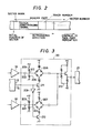
- Fig. 3 shows an example of the switching circuit 20.
- the signals amplified by the header signal side amplifier 16 and the magnetic signal side amplifier 19 have direct currents cut by capacitors 201 and 202, respectively. They are thereafter turned by resistors 203, 204 and resistors 205, 206 into signals which center round a middle point potential V/2 and which are input to diode switches 207 and 208, respectively.
- the diode switches are turned 'on' and 'off' by the switching signal 18 from the timing generator circuit 17.
- the switching circuit 20 in the present embodiment has been exemplified as the arrangement composed of the diode switches 207 and 208, it may well be constructed of analog switches of high speed.
- the period of time required for the switching needs to be selected in consideration of the data transfer rate of the system. For example, in a case where the transfer rate is on the order of several hundred kilobytes per second, the switching speed needs to be below one hundred nanoseconds.
- the switching period of time is experimentally determined, and is finally judged on the basis of verification with the actual signal processing circuit.
- FIG. 5 shows processes in the photodetectors et seq. as a block diagram.
- the arrangement before the photodetectors 10 and 13 in Fig. 1 applies also to the second embodiment, and is not illustrated.
- a switching control circuit 22 is so operated that the signal from the side of the photodetector 13 passes through the switching circuit 20 and enters the level slice circuit 21 as well as the sector mark detection circuit 15 at the posterior stage without fail during the period of time since the issue of the access instruction signal 23 till the end of the access operation.
- the switching control circuit 22 is reset so as to operate the switching circuit 20 in accordance with the gate signal 218 from the timing generator circuit 17 again.
- the access instruction signal 23 the gate signal 218, a switching signal 24, and the input/output signals of the switching circuit 20.
- the switching signal 24 is forcibly dropped to the "low” level irrespective of the state of the gate signal 218. Accordingly, the switching circuit 20 is selected so that only the signal on the header part reading photodetector side may pass therethrough at all times.
- the ordinary switching operation before the access is repeated again.
- the timing of the switching is based on a sector mark which is detected from a signal having passed through a change-over switch circuit, but the change-over switch is forcibly set so as to infallibly pass the signal from the header reading photodetector during the access operation only and is reset to the ordinary switching operation at the time of the end of the access, whereby a similar effect can be achieved.
Abstract
Description
- The present invention relates to a magnetic-optical disc memory system, and more particularly to a magnetic-optical disc file system which is well suited to stabilize a switching operation that is performed when a header signal and a data signal are detected.by separate photodetection means and are switched and synthesized in case of writing or erasing data in sector unit.
- An example of a magnetic-optical information recording and reproducing system, in which data is written or erased by a thermomagnetic effect and is read out by a magnetooptical effect, has been proposed in 'Technical Report of Electronics and Communications Society (in Japan)' CPM 83-53, pp. 13 - 19. This system employs a recording medium in which data is written with a magnetic signal, while address information is written with a phase signal in the form of embossed pits. As regards a read-out signal detecting system, however, the proposal does not refer to a method of processing both the data and address information items, namely, switching them.
- One of the inventors of the present invention has already proposed, with joint inventors who are not the inventors of the present invention, a magnetic-optical disc memory system in which detection means for a header signal and detection means for a data signal are disposed separately from each other and in which switching means to selectively pass the respective outputs of both the detection means is further disposed in order to synthesize both the signals. The proposal is described in Japanese Patent Application Laid-open No. 136047 of 1985 (Japanese Patent Application No. 242006 of 1983) and U.S. Patent Application Serial No. 685123. This proposal, however, refers to nothing of the stabilization of the operation of switching both the signals.
- An object of the present invention is to provide a magnetic-optical disc memory system of the type writing or erasing data in sector unit, which is capable of reliable switching processing in a case where header information given as phase information and data information given as magnetic information in the magnetic-optical disc memory system are detected by separate detection means and are thereafter switched and synthesized so as to process them as a series of information items.
- In the magnetic-optical disc memory system according to the present invention, the header part of a magnetic-optical disc has an embossed face structure. The reproduction of the header part is performed by detecting the variation of the quantity of reflected light. The reproduction of the data part is performed in such a way that the direction of perpendicular magnetization is detected by utilizing a magnetooptical effect. In the magnetic-optical disc memory system according to the present invention, a detection system for reading the header part and a detection system for reading the data part are individually disposed. Output signals from the respective detection systems are selected by a switching circuit in correspondence with the header part and the data part, thereby to be controlled so as to form a series of information items. The switching circuit is started in accordance with a timing based on the point of time at which a sector mark has been recognized by directly supplying a sector mark detection circuit with the signal detected by the detection system for reading the header part.
- In the accompanying drawings;
- Fig. 1 is a diagram showing a first embodiment of a magnetic-optical disc memory system according to the present invention;
- Fig. 2 is a diagram showing an example of the information format of a header part;
- Fig. 3 is an arrangement diagram of a switching circuit for the header part and a data part;
- Fig. 4 is a diagram showing input signals to and an output signal from the switching circuit and the switching operation of the switching circuit;
- Fig. 5 is a diagram showing a second embodiment of the present invention;
- Fig. 6 is a time chart showing the operations of switching and synthesizing signals according to the arrangement of Fig. 5;
- Fig. 7 is a diagram showing an example of arrangement of a switching control circuit; and
- Fig. 8 is a time chart showing operations in Fig. 7.
- In a magnetic-optical disc, a header part is provided with controlling information in the form of embossed pits for the purpose of writing, reading out or erasing data in sector unit. The header part is constructed of a sector mark for recognizing the initial position of a sector, a track number and a sector number for indicating the address of the sector, a clock synchronizing signal, an error correction signal, etc. On the other hand, a data part ranges between the header part and the next header part. In the present invention, since a header reading detection system and a data reading detection system are separately comprised, any means needs to be used for adjusting the levels of the signals of both the.detection systems and for selecting the signal from either detection system in correspondence with each part.
- In a case where different kinds of signals such as a phase signal and a magnetic signal are detected by individual detection systems and then handled as a series of information items, the operations of switching both the signals and thereafter synthesizing them by any methods are required. For the control of the switching operation, several methods as described below are considered.
- For example, the surface of the disc is formed with encoded signals (embossed patterns) for rotation control, and the encoded signals are detected. Here, when the numbers and positions of the encoded patterns are brought into correspondence with the respective sectors on the disc beforehand, it is possible to recognize the header part and the data part on the basis of timings from the edge of the encoded signal and to operate a switching circuit so as to switch and synthesize the detection signals from the photodetectors separate from each other. This method, however, is unsuitable on account of such severe conditions that the encoded patterns and the positions of the respective sectors correspond exactly and that the operation of a timing generator circuit is stably performed without being affected by temperature characteristics etc.
- Considered as another method is an expedient wherein the sector mark is detected from a signal behind a switching circuit for the switching and synthesis and wherein the header part and the data part are switched according to a timing based on the detection of the mark. This method performs the switching operation of the switching circuit in accordance with the timing based on the signal of, so to speak, its own. Surely, in a case where a certain track is being steadily read out, the switching operation is normally performed. However, in a case where the quantity of light projected on the disc has increased as in the writing or erasing mode, or in a case where access is to be done from a certain track to another track, the sector mark and the header signal cannot be detected. Therefore, when the above process is performed with the change-over switch thrown on the data part side having no address information, a signal for throwing the change-over switch back to the header part side is not obtained, so that a malfunction occurs to make the continuation of subsequent processes impossible.
- According to the present invention, the photodetection signal on the header detection side is directly applied to a sector mark detection circuit before entering the change-over switch, and the change-over switch is operated according to a timing based on the generation of a mark detection signal indicating that the sector mark has been detected. Accordingly, the sector mark can be reliably detected after the end of the access to another track. Therefore, the disadvantage stated above can be solved.
- According to another embodiment of the present invention, in case of starting an access process, the change-over switch is set forcibly so as to pass the photodetection signal on the header detection side, whereupon the access is executed, and when the target track has been reached, the switching operation is performed in correspondence with the header part or the data part again. In that case, the sector mark is detected at a stage posterior to the switching circuit, and even when the change-over switch is operated according to a timing based on a mark detection signal, processes can be continued normally.
- Now, embodiments of the present invention will be described. A first embodiment is illustrated in Fig. 1. This figure is a diagram showing the schematic arrangement of a magnetic-optical disc memory system according to the present invention, and showing parts of a magnetic-optical head and signal detecting and processing systems for a magnetic-optical disc. A light beam emitted from a
diode laser 1 is turned by a collimatinglens 2 into a collimated beam, which is transformed by a triangular prism 3 into a beam which has a circular light intensity distribution in section. After passing through, abeam splitter 4, the beam is focused as a minute spot on a disc 6 provided with a recording film (perpendicular magnetic film), by a focusing lens 5. An electromagnetic coil 7 establishes a magnetic field for writing or erasing. Information is read out by detecting the Kerr rotation of reflected light. The reflected light from the disc 6 passes through the focusing lens 5 again, and is thereafter reflected by thebeam splitter 4. The reflected light is further reflected by a beam splitter 8 and then passed through ananalyzer 9, and the analyzed light is led via a lens to aphotodetector 10, by which magnetic information and header information are detected. - It is convenient that the header information is previously provided in the form of embossed pits when the disc is fabricated. The reason is that the header information signifies information items such as sector marks which serve for recognizing the initial positions of respective sectors and clocking signals, track Nos. and sector Nos. which are required when decoding data, and that in general, a user need not alter the information items.
- Light transmitted through the beam splitter 8 is branched by a beam splitter 11 into two parts, one of which is guided to a
photodetector 12 for autofocus control and the other of which is guided to aphotodetector 13 for tracking control. By way of example, the light reflected by the beam splitter 11 is passed through an astigmatic optical system consisting of a spherical lens and a cylindrical lens and is partly isolated by a knife edge, whereupon it is led to thephotodetector 12 for detecting a focus error. On the other hand, the light transmitted through the beam splitter 11 is led via a spherical lens to the two-segmentedphotodetector 13 for detecting tracking errors. - The optical signal to be received by the
photodetector 13 is a signal modulated with the magnitudes of the quantity of the reflected light from the disc 6. That is, the header information provided on the disc 6 in the form of the embossed pits can be detected, not only by thephotodetector 10, but also by thephotodetector 13. The signal light to fall on thephotodetector 13 has not passed through theanalyzer 9, and therefore has the merit that it is less liable to be affected by the retardation of the disc 6 and the disturbance of polarization caused by the distribution of magnetization. Accordingly, it is more preferable to employ the signal on the side of thephotodetector 13 for the reading of the header information. Of course, the signal on the side of thephotodetector 10 must be employed for the magnetic information because the rotation of a polarization plane is detected. - The laser radiation optical system, the magnetic signal detection system, the header signal detection system and the electromagnetic coil constitute a magneto-optical head..This magneto-optical head is so constructed as to be movable to any desired radial position of the disc 6 by means of a step motor or linear motor (not shown).
- Here, the format of the header information will be somewhat described. Fig. 2 shows an example of the format of the header information. Although header information items need not always be in the format and sequence as shown in Fig. 2 to the end of performing the present invention, only a sector mark should be provided at the initial position of a sector for convenience' sake. Further, the number of bits of each constituent of the header information may be as desired.
- Next, there will be described a sector mark detection circuit system which forms the essential point of the present invention, and processing methods which concern the branching of the signal to this detection circuit system and the switching and synthesis between the magnetic information and the header information.
- In the arrangement of Fig. 1, the optical signal received by the header
signal detecting photodetector 13 is amplified to a proper level by anamplifier 14, and the amplified signal is branched to a sectormark detection circuit 15 and a variable-gain amplifier 16 for adjusting the level of the header signal to that of the signal of the magnetic information. When the sector mark has been recognized by the sectormark detection circuit 15, asignal 18 for the switching between a header part and a data part is generated by atiming generator circuit 17 which serves to determine the limits of the data part (the extent from the header part and the initial position of the next sector). On the other hand, the magnetooptical signal (data signal) received by the magneticsignal detecting photodetector 10 is amplified by anamplifier 19 and is thereafter sent to aswitching circuit 20 for switching the header part and the data part. In response to the switchingsignal 18, the switchingcircuit 20 switches signals so as to pass the signal from thephotodetector 13 as regards the header part and to pass the signal from thephotodetector 10 as regards the data part. Thereafter, the output of the switchingcircuit 20 is processed by alevel slice circuit 21, and the resulting digital signal is sent to the processing system of the next stage. - The foregoing is the first embodiment of the present invention, and the
timing generator circuit 17 as well as the switchingcircuit 20 will now be somewhat described. Since the sectormark detection circuit 15 itself is an already known circuit and does not require any special alteration in regard to the present embodiment, it shall be omitted from description. - Fig. 3 shows an example of the switching
circuit 20. The signals amplified by the headersignal side amplifier 16 and the magneticsignal side amplifier 19 have direct currents cut bycapacitors resistors resistors diode switches signal 18 from thetiming generator circuit 17. - When the
signal 18 from thetiming generator circuit 17 is at a "low" level, aninverter 209 renders the base of a transistor switch 210 a high level to turn "on" this transistor switch, so that thediode switch 207 is enabled. Meantime, the base of atransistor switch 211 is at the low level, so that thediode switch 208 is disabled. Accordingly, only the header signal is sent to the next stage. Conversely, when thesignal 18 from thetiming generator circuit 17 is at a "high" level, thediode switch 207 is disabled, and thediode switch 208 is enabled. Therefore, only the data signal is sent to the next stage. The signal selected by the diode switch passes through abuffer circuit 212, and is thereafter sent to thelevel slice circuit 21. Thebuffer circuit 212 is intended to lower the output impedance of the switchingcircuit 20 and to stably transmit the signals. Although it is illustrated as an emitter follower circuit by way of example, it may well be another circuit having the same effect. - In Fig. 3, the
timing generator circuit 17 receives the sector mark detection signal generated and defines the limits of the data part with a counter. That is, it counts fixed numbers of clocks, thereby to generate the digital gate signals of the "low" level for the header part and the "high" level for the data part by way of example. Of course, even when the "high" level is output for the header part and the "low" level for the data part contrariwise, a similar operation can be executed by reversing the operation of the switchingcircuit 20. - Fig. 4 shows the switching
signal 18 produced by thetiming generator circuit 17, and the situation of the switching between the header part and data part signals. - While the switching
circuit 20 in the present embodiment has been exemplified as the arrangement composed of the diode switches 207 and 208, it may well be constructed of analog switches of high speed. In this regard, the period of time required for the switching needs to be selected in consideration of the data transfer rate of the system. For example, in a case where the transfer rate is on the order of several hundred kilobytes per second, the switching speed needs to be below one hundred nanoseconds. The switching period of time is experimentally determined, and is finally judged on the basis of verification with the actual signal processing circuit. - Next, a second embodiment of the present invention will be described. Fig. 5 shows processes in the photodetectors et seq. as a block diagram. The arrangement before the
photodetectors - Referring to Fig. 5, the magnetic information of the data part received by the
photodetector 10 is amplified by theamplifier 19. On the other hand, the phase information of the header part received by thephotodetector 13 is amplified by theamplifier 14, and the level of the amplified signal is thereafter adjusted to the level of the magnetic information by the variable-gain amplifier 16. Both the signals are selected by the switchingcircuit 20. The output of the switchingcircuit 20 is, on one hand, processed and digitized by thelevel slice circuit 21. On the other hand, it is branched to the sectormark detection circuit 15. When the sector mark in the header part has been detected, agate signal 218 for switching the header part and the data part is output by thetiming generator circuit 17. Meanwhile, the instruction of the access operation ought to be issued from an upper controller (control unit). Therefore, a switchingcontrol circuit 22 is so operated that the signal from the side of thephotodetector 13 passes through the switchingcircuit 20 and enters thelevel slice circuit 21 as well as the sectormark detection circuit 15 at the posterior stage without fail during the period of time since the issue of theaccess instruction signal 23 till the end of the access operation. When theaccess instruction signal 23 has stopped, the switchingcontrol circuit 22 is reset so as to operate the switchingcircuit 20 in accordance with thegate signal 218 from thetiming generator circuit 17 again. Here, reference will be had to a time chart concerning the parts which are not included in the first embodiment and which are added in the second embodiment, namely, theaccess instruction signal 23, thegate signal 218, a switchingsignal 24, and the input/output signals of the switchingcircuit 20. - Fig. 6 is the time chart showing the operations pertinent to the second embodiment. In Fig. 6, the
signal 23 is rendered the "high" level in the absence of the access instruction. When theaccess instruction signal 23 is at the "high" level, thegate signal 218 is generated by thetiming generator circuit 17 in accordance with the timing based on the time of generation of a sectormark detection signal 25, as the "low" level for the header part and the "high" level for the data part, whereby the ordinary switching operation is performed. Here, let's consider a case where the access instruction has been given. At this time, theaccess instruction signal 23 changes from the "high" level to the "low" level. - 1 Simultaneously, the switching
signal 24 is forcibly dropped to the "low" level irrespective of the state of thegate signal 218. Accordingly, the switchingcircuit 20 is selected so that only the signal on the header part reading photodetector side may pass therethrough at all times. When, after the end of the access operation and the return of theaccess instruction signal 23 to the "high" level, the first sector mark has been detected, the ordinary switching operation before the access is repeated again. - Fig. 7 is a diagram showing an example of arrangement of the switching
control circuit 22. In the figure, numeral 30 designates a delay circuit which utilizes a counter. When supplied with the sectormark detection signal 25, thedelay circuit 30 delivers adetection signal 31 which is delayed by a time interval till the initial position of the data part succeeding the header part. Since the delayeddetection signal 31 is input to the reset (R) terminal of a flip-flop 33 through aninverter 32, theQ output 34 of the flip-flop 33 is held at the "high" level. Accordingly, in the state in which the sector mark is detected, oneinput 34 of an ANDcircuit 35 is at the "high" level, so that thegate signal 218 is delivered as the switchingsignal 24 as it is. - If the access operation has started, the
access instruction signal 23 becomes the "low" level which is passed through aninverter 36, and the "high" level is applied to the trigger (T) input of the flip-flop 33. Here, the D input and set .(S) input of the flip-flop 33 are pulled up to the "high" level (VOH). Therefore, the Q output of the flip-flop becomes the "low" level in response to the rise of the T input. Accordingly, even when the level of thegate signal 218 is the "high" level, the switchingsignal 24 is forced to become the "low" level, and hence, the switchingcircuit 20 is set so as to pass the signal on the header part detection side therethrough. When, after the end of the access operation, the sectormark detection signal 25 has been detected, the switchingcircuit 20 is reset again to the ordinary switching operation corresponding to the header part and the data part. While the flip-flop 33 included in the present embodiment is the D-type flip-flop, it may well be a flip-flop of a different type. Besides, whether or not theinverters - Fig. 8 shows the logic operations of the switching
control circuit 22 in Fig. 7 in correspondence with the above description. - In a case where a magnetic-optical disc of the type in which header parts are provided on the disc in the form of embossed pits, while data parts are written in magnetic directions, is handled in a magnetic-optical disc file system in which a header part reading photodetector and a data part reading photodetector are separately disposed, one embodiment of the present invention controls the timings at which signals from both the detectors are switched and synthesized, on the basis of the signal which is applied directly from the header part reading photodetector. Thus, according to the present invention, even when the reading of the header part is interrupted by an access operation and the system is reset again, the switching operation is promptly restarted, and hence, data can be stably and reliably written, read out and erased in sector unit. Besides, according to another embodiment of the present invention, the timing of the switching is based on a sector mark which is detected from a signal having passed through a change-over switch circuit, but the change-over switch is forcibly set so as to infallibly pass the signal from the header reading photodetector during the access operation only and is reset to the ordinary switching operation at the time of the end of the access, whereby a similar effect can be achieved.
Claims (4)
Applications Claiming Priority (2)
| Application Number | Priority Date | Filing Date | Title |
|---|---|---|---|
| JP60008980A JPH07105081B2 (en) | 1985-01-23 | 1985-01-23 | Magneto-optical disk device and information processing method thereof |
| JP8980/85 | 1985-01-23 |
Publications (3)
| Publication Number | Publication Date |
|---|---|
| EP0189187A2 true EP0189187A2 (en) | 1986-07-30 |
| EP0189187A3 EP0189187A3 (en) | 1988-03-30 |
| EP0189187B1 EP0189187B1 (en) | 1989-11-08 |
Family
ID=11707835
Family Applications (1)
| Application Number | Title | Priority Date | Filing Date |
|---|---|---|---|
| EP86100813A Expired EP0189187B1 (en) | 1985-01-23 | 1986-01-22 | Magnetic-optical disc memory system |
Country Status (6)
| Country | Link |
|---|---|
| US (1) | US4730289A (en) |
| EP (1) | EP0189187B1 (en) |
| JP (1) | JPH07105081B2 (en) |
| KR (1) | KR900000019B1 (en) |
| CN (1) | CN86100902B (en) |
| DE (1) | DE3666891D1 (en) |
Cited By (6)
| Publication number | Priority date | Publication date | Assignee | Title |
|---|---|---|---|---|
| GB2196467A (en) * | 1986-10-11 | 1988-04-27 | London Weekend Television | Optical disc with added magnetic record/playback facility |
| EP0322817A2 (en) * | 1987-12-25 | 1989-07-05 | Hitachi, Ltd. | Recording method for magnetoptical disk and apparatus therefor |
| FR2636763A1 (en) * | 1988-09-20 | 1990-03-23 | Sony Corp | |
| EP0409649A2 (en) * | 1989-07-21 | 1991-01-23 | Sharp Kabushiki Kaisha | Information recording and reproducing device |
| EP0432976A2 (en) * | 1989-12-11 | 1991-06-19 | International Business Machines Corporation | Magnetooptic data storage apparatus and magnetooptic disk |
| EP0599387A1 (en) * | 1992-11-20 | 1994-06-01 | Koninklijke Philips Electronics N.V. | Magneto-optical read/write device |
Families Citing this family (25)
| Publication number | Priority date | Publication date | Assignee | Title |
|---|---|---|---|---|
| US5189651A (en) * | 1986-05-12 | 1993-02-23 | Pioneer Electronic Corporation | Optical system in magneto-optical recording and reproducing device |
| JP2574765B2 (en) * | 1986-07-09 | 1997-01-22 | 株式会社日立製作所 | Magneto-optical disk device |
| JP2779409B2 (en) * | 1986-08-26 | 1998-07-23 | キヤノン株式会社 | Electron beam irradiation position detecting device and information recording / reproducing device using the same |
| US4967403A (en) * | 1986-08-25 | 1990-10-30 | Sony Corporation | Multi-format optical disk and reading device |
| US5251196A (en) * | 1987-09-30 | 1993-10-05 | Deutsche Thomson-Brandt Gmbh | Optical pick-up selectively reading and writing an optical and magneto-optical recorded medium |
| US4916680A (en) * | 1986-12-22 | 1990-04-10 | International Business Machines Corporation | Magnetooptic recording member having selectively-reversed erasure directions in predetermined recording areas of the record member |
| US4937800A (en) * | 1986-12-22 | 1990-06-26 | International Business Machines Corporation | Method of recording using selective-erasure directions for magnetooptic record members |
| US5051970A (en) * | 1987-05-08 | 1991-09-24 | Nippon Telegraph And Telephone Corporation | Magneto-optic recording system with overwrite capability |
| US5020040A (en) * | 1987-06-24 | 1991-05-28 | Digital Equipment Corporation | Overwriting system for magneto-optical recording with self timing track |
| US5043960A (en) * | 1987-09-25 | 1991-08-27 | Hitachi, Ltd. | Overwritable magneto-optic recording and reproducing apparatus |
| DE3732875A1 (en) * | 1987-09-30 | 1989-04-20 | Thomson Brandt Gmbh | OPTICAL RECORD CARRIER |
| US4931635A (en) * | 1987-12-01 | 1990-06-05 | Teijin Seiki Company Limited | Optical position sensor using Faraday effect element and magnetic scale |
| US4931634A (en) * | 1987-12-28 | 1990-06-05 | Teijin Seiki Company Limited | Optical position sensor using Kerr effect and a magnetic scale |
| US5166913A (en) * | 1988-01-27 | 1992-11-24 | Nec Corporation | Optical disk device for record and reproduction of additional information besides reproducing of basic information |
| US5034934A (en) * | 1988-07-15 | 1991-07-23 | Pioneer Electronic Corp. | Opto-magnetic disk unit with improved dynamic range characteristics and opto-magnetic disk therefor |
| JPH03171453A (en) * | 1989-11-29 | 1991-07-24 | Sony Corp | Magneto-optical signal reproducing method |
| US5272692A (en) * | 1989-12-11 | 1993-12-21 | International Business Machines Corporation | Data storage member having areas in which intensity-modulated signals are overlaid with magneto-optically recorded signals |
| US5245598A (en) * | 1990-06-27 | 1993-09-14 | Burroughs Alan C | Method and apparatus for seek operations in an optical recording system including holding a focus error signal at track crossings |
| JP2959588B2 (en) * | 1991-02-14 | 1999-10-06 | ソニー株式会社 | Magneto-optical disk and method of recording and reproducing sector management information thereof |
| JP2698303B2 (en) * | 1992-12-07 | 1998-01-19 | 三洋電機株式会社 | Recordable disk and disk recording device |
| JP2738304B2 (en) * | 1994-08-03 | 1998-04-08 | 株式会社日立製作所 | Signal processing method and apparatus |
| US6118753A (en) * | 1996-08-13 | 2000-09-12 | Hewlett-Packard Company | Erasable digital video disk with reference clock track |
| US6118632A (en) * | 1997-02-12 | 2000-09-12 | International Business Machines Corporation | Magnetic disk stack having laser-bump identifiers on magnetic disks |
| JP2000182241A (en) * | 1998-12-16 | 2000-06-30 | Hitachi Ltd | Head amplifier and optical disk device using it |
| JP4183868B2 (en) * | 1999-12-07 | 2008-11-19 | 富士通株式会社 | Optical storage device |
Citations (4)
| Publication number | Priority date | Publication date | Assignee | Title |
|---|---|---|---|---|
| JPS58114343A (en) * | 1981-12-26 | 1983-07-07 | Fujitsu Ltd | Optical recording and reproducing medium |
| JPS58118044A (en) * | 1981-12-31 | 1983-07-13 | Nec Corp | Medium recording system |
| JPS5977648A (en) * | 1982-10-26 | 1984-05-04 | Sharp Corp | Photomagnetic storage element |
| JPS60136047A (en) * | 1983-12-23 | 1985-07-19 | Hitachi Ltd | Photomagnetic processing system |
Family Cites Families (9)
| Publication number | Priority date | Publication date | Assignee | Title |
|---|---|---|---|---|
| US4001883A (en) * | 1974-03-07 | 1977-01-04 | Honeywell Information Systems, Inc. | High density data storage on magnetic disk |
| GB1554641A (en) * | 1975-08-11 | 1979-10-24 | Casio Computer Co Ltd | Data-recording device |
| JPS5841578B2 (en) * | 1978-10-04 | 1983-09-13 | 株式会社日立製作所 | Control method for rotating storage device |
| US4229808A (en) * | 1978-12-21 | 1980-10-21 | Ncr Corporation | Method for recording multiple data segments on a storage disc with eccentricity factor |
| US4367497A (en) * | 1981-01-02 | 1983-01-04 | Sperry Corporation | Digital data formatting system for high density magnetic recording |
| JPS57140086A (en) * | 1981-02-23 | 1982-08-30 | Hitachi Ltd | Recording and reproducing circuit for vtr |
| US4443870A (en) * | 1981-10-15 | 1984-04-17 | Burroughs Corporation | Optical memory system providing track following |
| EP0081138B1 (en) * | 1981-12-01 | 1987-10-21 | Matsushita Electric Industrial Co., Ltd. | Optical recording and reproducing disc |
| JPS6085727U (en) * | 1983-11-18 | 1985-06-13 | 三洋電機株式会社 | information reading device |
-
1985
- 1985-01-23 JP JP60008980A patent/JPH07105081B2/en not_active Expired - Fee Related
- 1985-12-27 KR KR1019850009851A patent/KR900000019B1/en not_active IP Right Cessation
-
1986
- 1986-01-14 US US06/818,684 patent/US4730289A/en not_active Expired - Lifetime
- 1986-01-22 EP EP86100813A patent/EP0189187B1/en not_active Expired
- 1986-01-22 DE DE8686100813T patent/DE3666891D1/en not_active Expired
- 1986-01-23 CN CN86100902A patent/CN86100902B/en not_active Expired
Patent Citations (4)
| Publication number | Priority date | Publication date | Assignee | Title |
|---|---|---|---|---|
| JPS58114343A (en) * | 1981-12-26 | 1983-07-07 | Fujitsu Ltd | Optical recording and reproducing medium |
| JPS58118044A (en) * | 1981-12-31 | 1983-07-13 | Nec Corp | Medium recording system |
| JPS5977648A (en) * | 1982-10-26 | 1984-05-04 | Sharp Corp | Photomagnetic storage element |
| JPS60136047A (en) * | 1983-12-23 | 1985-07-19 | Hitachi Ltd | Photomagnetic processing system |
Non-Patent Citations (4)
| Title |
|---|
| PATENT ABSTRACTS OF JAPAN, vol. 7, no. 224 (P-227)[1369], 5thOctober 1983; & JP-A-58 114 343 (FUJITSU) 07-07-1983 * |
| PATENT ABSTRACTS OF JAPAN, vol. 7, no. 228 (P-228)[1373], 8th October 1983; & JP-A-58 118 044 (NIPPON DENKI) 13-07-1983 * |
| PATENT ABSTRACTS OF JAPAN, vol. 8, no. 188 (P-297)[1625], 29th August 1984; & JP-A-59 077 648 (SHARP) 04-05-1984 * |
| PATENT ABSTRACTS OF JAPAN, vol. 9, no. 304 (P-409)[2027], 30th November 1985; & JP-A-60 136 047 (HITACHI) 19-07-1985 * |
Cited By (12)
| Publication number | Priority date | Publication date | Assignee | Title |
|---|---|---|---|---|
| GB2196467A (en) * | 1986-10-11 | 1988-04-27 | London Weekend Television | Optical disc with added magnetic record/playback facility |
| EP0322817A2 (en) * | 1987-12-25 | 1989-07-05 | Hitachi, Ltd. | Recording method for magnetoptical disk and apparatus therefor |
| EP0322817A3 (en) * | 1987-12-25 | 1991-03-13 | Hitachi, Ltd. | Recording method for magnetoptical disk and apparatus therefor |
| US5060208A (en) * | 1987-12-25 | 1991-10-22 | Hitachi, Ltd. | Magnetooptical recording method and apparatus utilizing shift adjustment |
| FR2636763A1 (en) * | 1988-09-20 | 1990-03-23 | Sony Corp | |
| EP0409649A2 (en) * | 1989-07-21 | 1991-01-23 | Sharp Kabushiki Kaisha | Information recording and reproducing device |
| EP0409649A3 (en) * | 1989-07-21 | 1992-09-02 | Sharp Kabushiki Kaisha | Information recording and reproducing device |
| US5365501A (en) * | 1989-07-21 | 1994-11-15 | Sharp Kabushiki Kaisha | Information recording and reproducing device |
| EP0432976A2 (en) * | 1989-12-11 | 1991-06-19 | International Business Machines Corporation | Magnetooptic data storage apparatus and magnetooptic disk |
| EP0432976A3 (en) * | 1989-12-11 | 1991-12-27 | International Business Machines Corporation | Magnetooptic data storage apparatus and magnetooptic disk |
| EP0599387A1 (en) * | 1992-11-20 | 1994-06-01 | Koninklijke Philips Electronics N.V. | Magneto-optical read/write device |
| US5365508A (en) * | 1992-11-20 | 1994-11-15 | U.S. Philips Corporation | Magneto-optical read/write device |
Also Published As
| Publication number | Publication date |
|---|---|
| KR860006093A (en) | 1986-08-18 |
| JPH07105081B2 (en) | 1995-11-13 |
| EP0189187A3 (en) | 1988-03-30 |
| JPS61170938A (en) | 1986-08-01 |
| EP0189187B1 (en) | 1989-11-08 |
| DE3666891D1 (en) | 1989-12-14 |
| CN86100902B (en) | 1988-12-14 |
| KR900000019B1 (en) | 1990-01-18 |
| CN86100902A (en) | 1986-08-20 |
| US4730289A (en) | 1988-03-08 |
Similar Documents
| Publication | Publication Date | Title |
|---|---|---|
| US4730289A (en) | Magnetic-optical disc memory system and apparatus for switching header and data information | |
| US4890273A (en) | Optical information recording/reproducing system with variable gain servo error correction in response to detected track formats | |
| JP2655682B2 (en) | Magneto-optical information recording / reproducing device | |
| US4879703A (en) | Magneto-optic memory apparatus with defect detection of recording medium during erasing operation | |
| KR960000826B1 (en) | Servo circuit for an optical disk information recording & | |
| KR900008378B1 (en) | Optical recording apparatus | |
| US5107473A (en) | Optical recording/reproducing device using permissible ranges for the value of an automatic gain control voltage | |
| US5060218A (en) | Write-once type optical recording/reproducing device | |
| EP0182127B1 (en) | System for preventing the overwriting of previously optically recorded data and for reading optically recorded data during writing | |
| US4982392A (en) | Stabilized optical pick-up device inhibiting the effect of the focus error signal at the start and end of a data region | |
| US5107101A (en) | Optical information processing apparatus with peak hold circuit for gain control signal | |
| EP0303936A2 (en) | Method and apparatus for optical recording and reproduction | |
| US5513159A (en) | Device for selecting magnetic head to be operated together with an optical head | |
| US5283775A (en) | Split detector system for direct read-while-write operation on magneto-optic media | |
| US4789972A (en) | Selectively controlling the erasure in a magneto-optic recording medium | |
| JP2795744B2 (en) | Single laser recording direct playback system (DRAW) | |
| EP0384358A2 (en) | Optical recording and playback system of dual light source type | |
| US5420835A (en) | Magneto-optic disk apparatus | |
| US6584050B1 (en) | Optical recording device, optical reproducing device, and optical memory medium | |
| US4916680A (en) | Magnetooptic recording member having selectively-reversed erasure directions in predetermined recording areas of the record member | |
| JP2738304B2 (en) | Signal processing method and apparatus | |
| JP3770789B2 (en) | Magneto-optical recording / reproducing apparatus | |
| US4937800A (en) | Method of recording using selective-erasure directions for magnetooptic record members | |
| JPS6310322A (en) | Optical disc device | |
| JPS621135A (en) | Optical card information recording and reproducing device |
Legal Events
| Date | Code | Title | Description |
|---|---|---|---|
| PUAI | Public reference made under article 153(3) epc to a published international application that has entered the european phase |
Free format text: ORIGINAL CODE: 0009012 |
|
| AK | Designated contracting states |
Kind code of ref document: A2 Designated state(s): DE NL |
|
| PUAL | Search report despatched |
Free format text: ORIGINAL CODE: 0009013 |
|
| AK | Designated contracting states |
Kind code of ref document: A3 Designated state(s): DE NL |
|
| 17P | Request for examination filed |
Effective date: 19880405 |
|
| 17Q | First examination report despatched |
Effective date: 19880706 |
|
| GRAA | (expected) grant |
Free format text: ORIGINAL CODE: 0009210 |
|
| AK | Designated contracting states |
Kind code of ref document: B1 Designated state(s): DE NL |
|
| REF | Corresponds to: |
Ref document number: 3666891 Country of ref document: DE Date of ref document: 19891214 |
|
| PLBE | No opposition filed within time limit |
Free format text: ORIGINAL CODE: 0009261 |
|
| STAA | Information on the status of an ep patent application or granted ep patent |
Free format text: STATUS: NO OPPOSITION FILED WITHIN TIME LIMIT |
|
| 26N | No opposition filed | ||
| PGFP | Annual fee paid to national office [announced via postgrant information from national office to epo] |
Ref country code: NL Payment date: 20030106 Year of fee payment: 18 |
|
| PGFP | Annual fee paid to national office [announced via postgrant information from national office to epo] |
Ref country code: DE Payment date: 20030310 Year of fee payment: 18 |
|
| PG25 | Lapsed in a contracting state [announced via postgrant information from national office to epo] |
Ref country code: NL Free format text: LAPSE BECAUSE OF NON-PAYMENT OF DUE FEES Effective date: 20040801 |
|
| PG25 | Lapsed in a contracting state [announced via postgrant information from national office to epo] |
Ref country code: DE Free format text: LAPSE BECAUSE OF NON-PAYMENT OF DUE FEES Effective date: 20040803 |
|
| NLV4 | Nl: lapsed or anulled due to non-payment of the annual fee |
Effective date: 20040801 |