EP0188751B1 - Connector socket - Google Patents
Connector socket Download PDFInfo
- Publication number
- EP0188751B1 EP0188751B1 EP85116034A EP85116034A EP0188751B1 EP 0188751 B1 EP0188751 B1 EP 0188751B1 EP 85116034 A EP85116034 A EP 85116034A EP 85116034 A EP85116034 A EP 85116034A EP 0188751 B1 EP0188751 B1 EP 0188751B1
- Authority
- EP
- European Patent Office
- Prior art keywords
- block
- socket
- bores
- contact elements
- contact
- Prior art date
- Legal status (The legal status is an assumption and is not a legal conclusion. Google has not performed a legal analysis and makes no representation as to the accuracy of the status listed.)
- Expired
Links
- 239000012212 insulator Substances 0.000 claims description 17
- 239000002184 metal Substances 0.000 claims description 3
- 241000251468 Actinopterygii Species 0.000 description 2
- 238000004519 manufacturing process Methods 0.000 description 2
- 239000000463 material Substances 0.000 description 2
- 229910001369 Brass Inorganic materials 0.000 description 1
- 230000000712 assembly Effects 0.000 description 1
- 238000000429 assembly Methods 0.000 description 1
- 239000010951 brass Substances 0.000 description 1
- 239000012634 fragment Substances 0.000 description 1
- 230000001771 impaired effect Effects 0.000 description 1
- 238000009413 insulation Methods 0.000 description 1
- 230000007257 malfunction Effects 0.000 description 1
- 238000007747 plating Methods 0.000 description 1
Images
Classifications
-
- H—ELECTRICITY
- H01—ELECTRIC ELEMENTS
- H01R—ELECTRICALLY-CONDUCTIVE CONNECTIONS; STRUCTURAL ASSOCIATIONS OF A PLURALITY OF MUTUALLY-INSULATED ELECTRICAL CONNECTING ELEMENTS; COUPLING DEVICES; CURRENT COLLECTORS
- H01R12/00—Structural associations of a plurality of mutually-insulated electrical connecting elements, specially adapted for printed circuits, e.g. printed circuit boards [PCB], flat or ribbon cables, or like generally planar structures, e.g. terminal strips, terminal blocks; Coupling devices specially adapted for printed circuits, flat or ribbon cables, or like generally planar structures; Terminals specially adapted for contact with, or insertion into, printed circuits, flat or ribbon cables, or like generally planar structures
- H01R12/70—Coupling devices
- H01R12/71—Coupling devices for rigid printing circuits or like structures
- H01R12/712—Coupling devices for rigid printing circuits or like structures co-operating with the surface of the printed circuit or with a coupling device exclusively provided on the surface of the printed circuit
- H01R12/716—Coupling device provided on the PCB
- H01R12/718—Contact members provided on the PCB without an insulating housing
-
- H—ELECTRICITY
- H01—ELECTRIC ELEMENTS
- H01R—ELECTRICALLY-CONDUCTIVE CONNECTIONS; STRUCTURAL ASSOCIATIONS OF A PLURALITY OF MUTUALLY-INSULATED ELECTRICAL CONNECTING ELEMENTS; COUPLING DEVICES; CURRENT COLLECTORS
- H01R13/00—Details of coupling devices of the kinds covered by groups H01R12/70 or H01R24/00 - H01R33/00
- H01R13/02—Contact members
- H01R13/15—Pins, blades or sockets having separate spring member for producing or increasing contact pressure
- H01R13/187—Pins, blades or sockets having separate spring member for producing or increasing contact pressure with spring member in the socket
-
- H—ELECTRICITY
- H01—ELECTRIC ELEMENTS
- H01R—ELECTRICALLY-CONDUCTIVE CONNECTIONS; STRUCTURAL ASSOCIATIONS OF A PLURALITY OF MUTUALLY-INSULATED ELECTRICAL CONNECTING ELEMENTS; COUPLING DEVICES; CURRENT COLLECTORS
- H01R13/00—Details of coupling devices of the kinds covered by groups H01R12/70 or H01R24/00 - H01R33/00
- H01R13/02—Contact members
- H01R13/10—Sockets for co-operation with pins or blades
- H01R13/11—Resilient sockets
- H01R13/111—Resilient sockets co-operating with pins having a circular transverse section
Definitions
- This invention relates to an improved electrical connector.
- Dual-in-line packages are made up of dual-in-line packages, each having a plurality of pins extending therefrom. Such components have gained wide acceptance in the electronics industry. These dual-in-line packages are normally mounted on a circuit board for making connection to various other components.
- One system utilized in mounting dual-in-line packages to circuit boards is through the use of dual-in-line connector assemblies which include an insulator block having a plurality of pin-receiving apertures and corresponding electrical sockets. These sockets receive pins from the dual-in-line package of the integrated circuit for making electrical contact.
- a typical dual-in-line package or integrated circuit and connector or socket assembly is shown in Doucet, Patent 4,004,196. Such a system is manufactured by Garry Manufacturing Company of New Brunswick, New Jersey, and sold as their Series 610.
- a typical connector assembly as shown in Doucet is assembled by first assembling the socket and then inserting the contact into the plastic body or insulator frame.
- the socket is spaced upwardly from the plastic body and has a contact-to- contact spacing of about 0.25 cm (0.100 inch).
- the electrical integrity may be impaired by metal fragments, for example, from the component coming into contact with the socket or terminal on the face or top side of the assembly, possibly causing a circuit short or malfunction.
- pins from the component or integrated circuits are often bent when inserted into the socket because of a stepped lead-in entry hole which consists of two parts and a chamfer, or due to misalignment of the parts.
- an electrical connector comprising an insulator block having top and bottom faces and a plurality of spaced bores extending into the block from the bottom face thereof with top ends terminating below the top face of the block, said top face of the block having inwardly tapered mouths, radiating flat abutment shoulders at the terminal ends of said bores extending radially inward to the converging ends of the mouths, metal tubular sockets having open top bores with flat radial top edges and with closed bottom ends converging to reduced diameter axially extending pin portions, tubular contact elements having inwardly biased depending contact fingers in the bores spaced below said top edges, said tubular sockets being press fitted into said bores of the block from the bottom face of the block with their top edges bottomed against said shoulders and with the pin portions thereof extending beyond the bottom face of the block, and said shoulders overlying the top ends of said contact elements in the sockets whereby the top face of the block is free from projections, the tape
- the present invention improves the known electrical connector systems by providing an insulation block with closely spaced bores therethrough having tapered inlet mouths and receiving tubular sockets below these mouths so that the top face of the block is free from projections.
- the sockets have pin portions projecting from the bottom of the block and are equipped with contact elements for electrical components which are easily guided into locked engagement therewith by the tapered mouths of the bores.
- an electrical connector system which includes an insulator block and a plurality of closely-spaced sockets or terminals for receiving connector pins from electronic components such as integrated circuits (IC).
- Each of the socket terminals includes a body section and a lead for electrical connection to other components such as circuit boards.
- the insulator block has a plurality of closely-spaced pin-receiving apertures therein. At the pin-receiving end of the aperture, there is provided a conically-shaped inwardly tapering lead-in or chamfer which opens into a generally cylindrical socket-receiving portion of the block. Within the aperture, the tapering lead-in and the socket-receiving section define an inner abutment shoulder for use in positioning the socket within the aperture.
- the socket terminal includes an elongated sleeve-like body section and an elongated terminal or lead pin.
- the body section has a hollow tube-like interior for receiving a connector pin from an electronic device and an outer surface with gripping means thereon for gripping the aperture-forming wall.
- the axial position of the socket terminal within the aperture relative to the conical lead is defined by the abutment of the edge of the socket body section with the inner abutment shoulder.
- the socket gripping means engages the aperture forming wall so as to secure the socket in place.
- the electrical connector is characterised in that the inner diameter of the socket member is greater than the diameter of the inner end of the tapered mouth, thereby exposing the shoulder of the bore of the insulator block, the combined wall thickness of the socket member and contact element is greater than the radial width of the radial abutment shoulder, and the top end of said contact element is conically tapered to eliminate any internal abutment shoulder under the tapered mouth to cooperate with the tapered mouth for guiding an electrical component therein.
- a dual-in-line socket assembly 10 generally, which includes an insulator block 12 having top and bottom faces 12a and 12b and a plurality of aligned and closely-spaced pin-and-socket-receiving apertures, such as 14, 16 and 18, extending between the faces.
- Each of the apertures includes a conically-shaped inwardly tapering chamfer or countersink 20 in the top face of the insulator block, which acts as a lead-in or guide for pins associated with an electrical component such as an IC (integrated circuit) entering the pin-and-socket-receiving aperture.
- the remaining portion of the aperture is a socket-receiving cylindrical bore 22 which extends between the lead-in to the lower face 12b.
- the lead-in 20 opens into the cylindrical bore 22 and at the junction, the lead-in 20 has a smaller diameter than the bore section 22, so as to form an internal abutment shoulder 24.
- Each of the socket terminals such as 26 generally, includes a hollow tubular pin-receiving body section 28 and a terminal or lead end 30. Typically each of the socket terminals are machined from brass.
- the exterior surface of the socket body section includes a tapered lead-in or upper end 32 and a pair of grooves 34 and 36 which are shaped to form a barb or "fish hook" 38 for grasping the insulator block.
- the outer diameter of the socket body 28 is slightly larger than the inner diameter of the socket-receiving aperture 22 so that when the socket is inserted into the aperture, an interference or press fit results for holding the socket in place.
- the travel or positioning of the socket 26 is limited and defined by the engagement of the upper edge of the socket terminal 26 with the insulator block abutment shoulder 24.
- the socket 26 does not extend to or above the top face 12a of the insulator block, it is shorter in length than other socket terminals, requires less material to make, is less expensive to manufacture and requires less plating to assure excellent electric contact.
- An electric contact element 40 is positioned inside each of the socket terminals for making physical and electrical contact with the electrical component pins.
- the contact as seen in Figure 5 is a sleeve-like element which includes a ring-like upper section 42 and four depending resilient inwardly biased contact tabs or fingers such as 44.
- the outside diameter of the ring-like portion of the sleeve. 42 is slightly larger than the inside diameter of the socket terminal so as to require that the contact be press fitted into the inside of the socket terminal 26.
- the top edge of the contact is flush with the socket top edge. It will be noted that the top edge of the contact has a slight taper or lead-in 46.
- the inside diameter of the socket terminal approximates the inside diameter of the lead-in 20 and is generally axially aligned therewith. This alignment aids in guiding the electrical component pins into the socket terminal.
- an electrical component 50 is shown in dashed lines and includes a plurality of pins such as 52.
- the pins, such as 52 are inserted through the lead- ins, such as 20, into the socket 26.
- the press fit socket and fish hook grip 38 prevent downward axial movement of the socket.
- the pin 52 enters the lead-in, extends into the sleeve or ring portion 42 of the sleeve and then engages and contacts one or more of the inwardly biased resilient tabs 44.
Landscapes
- Connector Housings Or Holding Contact Members (AREA)
Description
- This invention relates to an improved electrical connector.
- Electrical components, such as integrated circuits, are made up of dual-in-line packages, each having a plurality of pins extending therefrom. Such components have gained wide acceptance in the electronics industry. These dual-in-line packages are normally mounted on a circuit board for making connection to various other components. One system utilized in mounting dual-in-line packages to circuit boards is through the use of dual-in-line connector assemblies which include an insulator block having a plurality of pin-receiving apertures and corresponding electrical sockets. These sockets receive pins from the dual-in-line package of the integrated circuit for making electrical contact.
- Numerous prior art patents disclose connectors and systems for making electrical contact. See, for example, U.S. Patents 3,335,357, Damen et al; 3,448,345, Koehler, Jr., et al; 3,717,841, Mancini; 4,004,196, Doucet; and 4,004,197, Hawkes, Jr.
- A typical dual-in-line package or integrated circuit and connector or socket assembly is shown in Doucet, Patent 4,004,196. Such a system is manufactured by Garry Manufacturing Company of New Brunswick, New Jersey, and sold as their Series 610.
- A typical connector assembly as shown in Doucet is assembled by first assembling the socket and then inserting the contact into the plastic body or insulator frame. Typically the socket is spaced upwardly from the plastic body and has a contact-to- contact spacing of about 0.25 cm (0.100 inch). In such situations the electrical integrity may be impaired by metal fragments, for example, from the component coming into contact with the socket or terminal on the face or top side of the assembly, possibly causing a circuit short or malfunction. Furthermore, pins from the component or integrated circuits are often bent when inserted into the socket because of a stepped lead-in entry hole which consists of two parts and a chamfer, or due to misalignment of the parts.
- In accordance with a first aspect of the present . invention, there is provided an electrical connector comprising an insulator block having top and bottom faces and a plurality of spaced bores extending into the block from the bottom face thereof with top ends terminating below the top face of the block, said top face of the block having inwardly tapered mouths, radiating flat abutment shoulders at the terminal ends of said bores extending radially inward to the converging ends of the mouths, metal tubular sockets having open top bores with flat radial top edges and with closed bottom ends converging to reduced diameter axially extending pin portions, tubular contact elements having inwardly biased depending contact fingers in the bores spaced below said top edges, said tubular sockets being press fitted into said bores of the block from the bottom face of the block with their top edges bottomed against said shoulders and with the pin portions thereof extending beyond the bottom face of the block, and said shoulders overlying the top ends of said contact elements in the sockets whereby the top face of the block is free from projections, the tapered mouths in the top face provide unobstructed lead-in guides for directing electrical components into the contact elements in firm contact with the fingers of the contact elements, and the projecting pin portions of the sockets provide spaced terminals, characterised in that said inwardly tapered mouths converge directly into the axial central top portions of the bores, the tubular contact elements are pressed into the upper ends of the socket bores having top edges flush with the top edges of the sockets, and the shoulders overlying the contact elements prevent pulling of the contact elements into the mouths by electrical components engaged by the fingers.
- The present invention improves the known electrical connector systems by providing an insulation block with closely spaced bores therethrough having tapered inlet mouths and receiving tubular sockets below these mouths so that the top face of the block is free from projections. The sockets have pin portions projecting from the bottom of the block and are equipped with contact elements for electrical components which are easily guided into locked engagement therewith by the tapered mouths of the bores.
- There is provided by this invention an electrical connector system which includes an insulator block and a plurality of closely-spaced sockets or terminals for receiving connector pins from electronic components such as integrated circuits (IC). Each of the socket terminals includes a body section and a lead for electrical connection to other components such as circuit boards.
- The insulator block has a plurality of closely-spaced pin-receiving apertures therein. At the pin-receiving end of the aperture, there is provided a conically-shaped inwardly tapering lead-in or chamfer which opens into a generally cylindrical socket-receiving portion of the block. Within the aperture, the tapering lead-in and the socket-receiving section define an inner abutment shoulder for use in positioning the socket within the aperture.
- The socket terminal includes an elongated sleeve-like body section and an elongated terminal or lead pin. The body section has a hollow tube-like interior for receiving a connector pin from an electronic device and an outer surface with gripping means thereon for gripping the aperture-forming wall. The axial position of the socket terminal within the aperture relative to the conical lead is defined by the abutment of the edge of the socket body section with the inner abutment shoulder. The socket gripping means engages the aperture forming wall so as to secure the socket in place.
- In accordance with a second aspect of the present invention the electrical connector is characterised in that the inner diameter of the socket member is greater than the diameter of the inner end of the tapered mouth, thereby exposing the shoulder of the bore of the insulator block, the combined wall thickness of the socket member and contact element is greater than the radial width of the radial abutment shoulder, and the top end of said contact element is conically tapered to eliminate any internal abutment shoulder under the tapered mouth to cooperate with the tapered mouth for guiding an electrical component therein.
- By way of example only, a specific embodiment of the present invention will now be described, with reference to the accompanying drawings, in which:
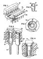
- Fig.1 is a perspective view showing a connector assembly having an insulator block with a plurality of apertures and socket terminals, along with an integrated circuit component whose pins are positioned to be inserted into sockets;
- Fig.2 is a sectional view taken along II-II of Fig.1 and showing the insulator block portion of the connector assembly in section with the left-hand socket terminal shown in section and the right-hand socket terminal shown in full;
- Fig.3 is a plan view of a pin-receiving socket showing the positioning of the socket terminal in the insulator block;
- Fig.4 is a greatly enlarged sectional view showing the upper portion of a socket terminal and a pin extending therein; and
- Fig.5 is a perspective view showing a socket contact for positioning within the socket terminal and for electrically contacting the component pin.
- Referring now to the drawings, there is now shown in Fig.1 a dual-in-line socket assembly 10 generally, which includes an
insulator block 12 having top andbottom faces - Each of the apertures includes a conically-shaped inwardly tapering chamfer or
countersink 20 in the top face of the insulator block, which acts as a lead-in or guide for pins associated with an electrical component such as an IC (integrated circuit) entering the pin-and-socket-receiving aperture. The remaining portion of the aperture is a socket-receivingcylindrical bore 22 which extends between the lead-in to thelower face 12b. - As can be seen from the drawings, the lead-in 20 opens into the
cylindrical bore 22 and at the junction, the lead-in 20 has a smaller diameter than thebore section 22, so as to form aninternal abutment shoulder 24. - Each of the socket terminals, such as 26 generally, includes a hollow tubular pin-receiving
body section 28 and a terminal orlead end 30. Typically each of the socket terminals are machined from brass. The exterior surface of the socket body section includes a tapered lead-in orupper end 32 and a pair ofgrooves - The outer diameter of the
socket body 28 is slightly larger than the inner diameter of the socket-receivingaperture 22 so that when the socket is inserted into the aperture, an interference or press fit results for holding the socket in place. The travel or positioning of thesocket 26 is limited and defined by the engagement of the upper edge of thesocket terminal 26 with the insulatorblock abutment shoulder 24. - It will be appreciated that since the
socket 26 does not extend to or above thetop face 12a of the insulator block, it is shorter in length than other socket terminals, requires less material to make, is less expensive to manufacture and requires less plating to assure excellent electric contact. - An
electric contact element 40 is positioned inside each of the socket terminals for making physical and electrical contact with the electrical component pins. The contact as seen in Figure 5 is a sleeve-like element which includes a ring-likeupper section 42 and four depending resilient inwardly biased contact tabs or fingers such as 44. The outside diameter of the ring-like portion of the sleeve. 42 is slightly larger than the inside diameter of the socket terminal so as to require that the contact be press fitted into the inside of thesocket terminal 26. When positioned in the socket terminal, the top edge of the contact is flush with the socket top edge. It will be noted that the top edge of the contact has a slight taper or lead-in 46. - Referring to Figure 4, it is seen that the inside diameter of the socket terminal approximates the inside diameter of the lead-in 20 and is generally axially aligned therewith. This alignment aids in guiding the electrical component pins into the socket terminal.
- Referring now to Figure 1, an
electrical component 50 is shown in dashed lines and includes a plurality of pins such as 52. In order to connect theelectronic component 50 to the socket assembly, the pins, such as 52, are inserted through the lead- ins, such as 20, into thesocket 26. The press fit socket andfish hook grip 38 prevent downward axial movement of the socket. Furthermore, as seen in Figure 4, thepin 52 enters the lead-in, extends into the sleeve orring portion 42 of the sleeve and then engages and contacts one or more of the inwardly biasedresilient tabs 44. - Among the advantages to this system is a reduction in the amount of material needed to make each socket, a reduction in the surface area required to be plated for electrical contact, accurate positioning of the connector in each of the apertures due to the positioning of the abutment shoulder, and a minimization of short circuiting or interconnection between the socket element by positioning all of the metallic contacts below the surface of the insulator block.
Claims (2)
Applications Claiming Priority (2)
| Application Number | Priority Date | Filing Date | Title |
|---|---|---|---|
| US686461 | 1984-12-26 | ||
| US06/686,461 US4620757A (en) | 1984-12-26 | 1984-12-26 | Connector socket |
Publications (2)
| Publication Number | Publication Date |
|---|---|
| EP0188751A1 EP0188751A1 (en) | 1986-07-30 |
| EP0188751B1 true EP0188751B1 (en) | 1989-05-31 |
Family
ID=24756390
Family Applications (1)
| Application Number | Title | Priority Date | Filing Date |
|---|---|---|---|
| EP85116034A Expired EP0188751B1 (en) | 1984-12-26 | 1985-12-16 | Connector socket |
Country Status (3)
| Country | Link |
|---|---|
| US (1) | US4620757A (en) |
| EP (1) | EP0188751B1 (en) |
| DE (1) | DE3570810D1 (en) |
Families Citing this family (21)
| Publication number | Priority date | Publication date | Assignee | Title |
|---|---|---|---|---|
| JPS6435879A (en) * | 1987-07-31 | 1989-02-06 | Texas Instruments Japan | Socket |
| US4934967A (en) * | 1987-12-15 | 1990-06-19 | Amp Incorporated | Socket for pin grid array |
| US4892492A (en) * | 1988-06-17 | 1990-01-09 | Modular Computer Systems, Inc. | Device with openings for receiving pins of electrical components |
| US5038467A (en) * | 1989-11-09 | 1991-08-13 | Advanced Interconnections Corporation | Apparatus and method for installation of multi-pin components on circuit boards |
| US4943846A (en) * | 1989-11-09 | 1990-07-24 | Amp Incorporated | Pin grid array having seperate posts and socket contacts |
| EP0476848B1 (en) * | 1990-09-07 | 1995-12-13 | ITT INDUSTRIES, INC. (a Delaware corporation) | Closed entry socket contact assembly |
| GB9209948D0 (en) * | 1992-05-08 | 1992-06-24 | Amp Gmbh | Electrical socket terminal |
| US5318465A (en) * | 1993-06-10 | 1994-06-07 | Burndy Corporation | Retention system with collapsible bridge |
| US5478257A (en) * | 1994-04-07 | 1995-12-26 | Burndy Corporation | Retention device |
| US5653601A (en) * | 1995-07-11 | 1997-08-05 | Molex Incorporated | Terminal socket assembly |
| US5742481A (en) * | 1995-10-04 | 1998-04-21 | Advanced Interconnections Corporation | Removable terminal support member for integrated circuit socket/adapter assemblies |
| TW438061U (en) * | 1999-04-16 | 2001-05-28 | Hon Hai Prec Ind Co Ltd | Electrical connector |
| US6586826B1 (en) | 2001-06-13 | 2003-07-01 | Amkor Technology, Inc. | Integrated circuit package having posts for connection to other packages and substrates |
| US6700800B2 (en) * | 2002-06-14 | 2004-03-02 | Intel Corporation | Retainer for circuit board assembly and method for using the same |
| FR2880997A1 (en) * | 2005-01-18 | 2006-07-21 | Souriau Soc Par Actions Simpli | INTERMEDIATE ELEMENT FOR ESTABLISHING A CONNECTION BETWEEN A CABLE AND A CONTACT ELEMENT, AND CONNECTOR ASSEMBLY |
| DE102006030135B4 (en) * | 2006-06-28 | 2008-05-08 | Mc Technology Gmbh | Device for mounting pins on a printed circuit board |
| EP1912295A1 (en) * | 2006-10-09 | 2008-04-16 | Delphi Technologies, Inc. | Bus bar |
| CN201113042Y (en) * | 2007-07-10 | 2008-09-10 | 富士康(昆山)电脑接插件有限公司 | Electric connector |
| US11128067B2 (en) * | 2018-11-01 | 2021-09-21 | Hubbell Incorporated | Electrical connector with adjustable alignment member |
| EP3704946A1 (en) | 2019-03-07 | 2020-09-09 | Viscofan, S.A. | Edible tubular food casings and method for their production |
| EP3732980A1 (en) | 2019-04-30 | 2020-11-04 | Viscofan, S.A. | Edible film and method for its manufacturing |
Family Cites Families (13)
| Publication number | Priority date | Publication date | Assignee | Title |
|---|---|---|---|---|
| US2907976A (en) * | 1956-07-27 | 1959-10-06 | Raytheon Co | Electrical connectors and contacts therefor |
| FR1280177A (en) * | 1960-12-21 | 1961-12-29 | Malco Mfg Co | Electrical connection terminals |
| US3383648A (en) * | 1965-08-20 | 1968-05-14 | Milton Ross Controls Co Inc | Miniature sockets |
| US3634879A (en) * | 1968-07-15 | 1972-01-11 | Amp Inc | Pin receptacle and carrier members therefor |
| US3717841A (en) * | 1972-05-18 | 1973-02-20 | Berg Electronics Inc | Socket terminal |
| US3957337A (en) * | 1975-02-21 | 1976-05-18 | Litton Systems, Inc. | Miniature electrical connector having contact centering means |
| DE2703010A1 (en) * | 1977-01-26 | 1978-07-27 | Grote & Hartmann | Plug board system for integrated circuits - has contact springs which have insertion loop at top, and soldering tags projecting downwards |
| US4274700A (en) * | 1977-10-12 | 1981-06-23 | Bunker Ramo Corporation | Low cost electrical connector |
| US4217024A (en) * | 1977-11-07 | 1980-08-12 | Burroughs Corporation | Dip socket having preloading and antiwicking features |
| US4166667A (en) * | 1978-04-17 | 1979-09-04 | Gte Sylvania, Incorporated | Circuit board connector |
| US4196957A (en) * | 1978-06-12 | 1980-04-08 | Gte Sylvania Incorporated | Circuit board connector |
| US4186990A (en) * | 1978-07-19 | 1980-02-05 | Augat Inc. | Lead socket insert |
| US4381134A (en) * | 1981-03-13 | 1983-04-26 | Bell Telephone Laboratories, Incorporated | Electrical connector for plated-through holes |
-
1984
- 1984-12-26 US US06/686,461 patent/US4620757A/en not_active Expired - Lifetime
-
1985
- 1985-12-16 EP EP85116034A patent/EP0188751B1/en not_active Expired
- 1985-12-16 DE DE8585116034T patent/DE3570810D1/en not_active Expired
Also Published As
| Publication number | Publication date |
|---|---|
| DE3570810D1 (en) | 1989-07-06 |
| EP0188751A1 (en) | 1986-07-30 |
| US4620757A (en) | 1986-11-04 |
Similar Documents
| Publication | Publication Date | Title |
|---|---|---|
| EP0188751B1 (en) | Connector socket | |
| CA1069197A (en) | Solderless electrical contact | |
| US4526429A (en) | Compliant pin for solderless termination to a printed wiring board | |
| US4660920A (en) | Printed circuit board connector | |
| US5362244A (en) | Socket having resilient locking tabs | |
| KR100550407B1 (en) | One Touch Connectors and One Touch Connector Assemblies | |
| US5960540A (en) | Insulated wire with integral terminals | |
| US3975072A (en) | Low profile integrated circuit connector and method | |
| US6071127A (en) | HF coaxial connector having a plug module and a socket module | |
| US6080008A (en) | Push-wire contact | |
| EP1082789B1 (en) | Threaded double sided compressed wire bundle connector | |
| EP0097018B1 (en) | Insulation displacement contact latching terminal | |
| US4534603A (en) | Assembly of a contact spring and wire wrap terminal | |
| CA2307922C (en) | Surface-mount electrical connection device | |
| EP0684756A2 (en) | Socket having an auxiliary electrical component mounted thereon | |
| US6077087A (en) | Coaxial connector module with an overmolded ground contact | |
| US5655930A (en) | Electrical pin field on a printed circuit board | |
| EP0109297B1 (en) | Improvements in electrical contact members and electrical connector assemblies | |
| US4784622A (en) | Stamped and formed contact | |
| EP0063023B1 (en) | A dual in-line socket assembly | |
| US4380119A (en) | Method of making an electrical connector assembly | |
| US3838203A (en) | Insertable electrical termination mounting | |
| EP0418045A1 (en) | Coaxial pin connector having an array of conductive hollow cylindrical structures | |
| EP0171985A2 (en) | Improvements in stacking connectors for printed circuit boards and in printed circuit board assemblies employing stacking connectors | |
| EP0139786B1 (en) | Press fit connector insulator and contact |
Legal Events
| Date | Code | Title | Description |
|---|---|---|---|
| PUAI | Public reference made under article 153(3) epc to a published international application that has entered the european phase |
Free format text: ORIGINAL CODE: 0009012 |
|
| AK | Designated contracting states |
Kind code of ref document: A1 Designated state(s): CH DE FR GB LI |
|
| 17P | Request for examination filed |
Effective date: 19870124 |
|
| 17Q | First examination report despatched |
Effective date: 19880418 |
|
| GRAA | (expected) grant |
Free format text: ORIGINAL CODE: 0009210 |
|
| AK | Designated contracting states |
Kind code of ref document: B1 Designated state(s): CH DE FR GB LI |
|
| REF | Corresponds to: |
Ref document number: 3570810 Country of ref document: DE Date of ref document: 19890706 |
|
| ET | Fr: translation filed | ||
| PGFP | Annual fee paid to national office [announced via postgrant information from national office to epo] |
Ref country code: CH Payment date: 19891229 Year of fee payment: 5 |
|
| PLBE | No opposition filed within time limit |
Free format text: ORIGINAL CODE: 0009261 |
|
| STAA | Information on the status of an ep patent application or granted ep patent |
Free format text: STATUS: NO OPPOSITION FILED WITHIN TIME LIMIT |
|
| 26N | No opposition filed | ||
| PG25 | Lapsed in a contracting state [announced via postgrant information from national office to epo] |
Ref country code: LI Effective date: 19901231 Ref country code: CH Effective date: 19901231 |
|
| REG | Reference to a national code |
Ref country code: CH Ref legal event code: PL |
|
| PGFP | Annual fee paid to national office [announced via postgrant information from national office to epo] |
Ref country code: FR Payment date: 19991202 Year of fee payment: 15 |
|
| PGFP | Annual fee paid to national office [announced via postgrant information from national office to epo] |
Ref country code: DE Payment date: 19991222 Year of fee payment: 15 |
|
| PG25 | Lapsed in a contracting state [announced via postgrant information from national office to epo] |
Ref country code: FR Free format text: LAPSE BECAUSE OF NON-PAYMENT OF DUE FEES Effective date: 20010831 |
|
| REG | Reference to a national code |
Ref country code: FR Ref legal event code: ST |
|
| PG25 | Lapsed in a contracting state [announced via postgrant information from national office to epo] |
Ref country code: DE Free format text: LAPSE BECAUSE OF NON-PAYMENT OF DUE FEES Effective date: 20011002 |
|
| REG | Reference to a national code |
Ref country code: GB Ref legal event code: IF02 |
|
| PGFP | Annual fee paid to national office [announced via postgrant information from national office to epo] |
Ref country code: GB Payment date: 20041104 Year of fee payment: 20 |
|
| PG25 | Lapsed in a contracting state [announced via postgrant information from national office to epo] |
Ref country code: GB Free format text: LAPSE BECAUSE OF EXPIRATION OF PROTECTION Effective date: 20051215 |
|
| REG | Reference to a national code |
Ref country code: GB Ref legal event code: PE20 |