EP0187778B1 - Adaptive hybrid circuit - Google Patents
Adaptive hybrid circuit Download PDFInfo
- Publication number
- EP0187778B1 EP0187778B1 EP85903138A EP85903138A EP0187778B1 EP 0187778 B1 EP0187778 B1 EP 0187778B1 EP 85903138 A EP85903138 A EP 85903138A EP 85903138 A EP85903138 A EP 85903138A EP 0187778 B1 EP0187778 B1 EP 0187778B1
- Authority
- EP
- European Patent Office
- Prior art keywords
- signal
- transmit
- receive
- output
- transmission line
- Prior art date
- Legal status (The legal status is an assumption and is not a legal conclusion. Google has not performed a legal analysis and makes no representation as to the accuracy of the status listed.)
- Expired
Links
Images


Classifications
-
- G—PHYSICS
- G06—COMPUTING; CALCULATING OR COUNTING
- G06G—ANALOGUE COMPUTERS
- G06G7/00—Devices in which the computing operation is performed by varying electric or magnetic quantities
- G06G7/12—Arrangements for performing computing operations, e.g. operational amplifiers
- G06G7/16—Arrangements for performing computing operations, e.g. operational amplifiers for multiplication or division
- G06G7/163—Arrangements for performing computing operations, e.g. operational amplifiers for multiplication or division using a variable impedance controlled by one of the input signals, variable amplification or transfer function
-
- H—ELECTRICITY
- H04—ELECTRIC COMMUNICATION TECHNIQUE
- H04B—TRANSMISSION
- H04B1/00—Details of transmission systems, not covered by a single one of groups H04B3/00 - H04B13/00; Details of transmission systems not characterised by the medium used for transmission
- H04B1/38—Transceivers, i.e. devices in which transmitter and receiver form a structural unit and in which at least one part is used for functions of transmitting and receiving
- H04B1/40—Circuits
- H04B1/54—Circuits using the same frequency for two directions of communication
- H04B1/58—Hybrid arrangements, i.e. arrangements for transition from single-path two-direction transmission to single-direction transmission on each of two paths or vice versa
-
- H—ELECTRICITY
- H04—ELECTRIC COMMUNICATION TECHNIQUE
- H04B—TRANSMISSION
- H04B3/00—Line transmission systems
- H04B3/02—Details
- H04B3/03—Hybrid circuits
Definitions
- This invention relates to adaptive hybrid circuits of the kind coupled to signal transmit means, and to signal receive means of a local station coupled to a signal transmission line, for adaptively minimizing crosstalk from said transmit means to said receive means including comparison means adapted to generate an adjustment control signal and adjustment means adapted to modify a signal from said transmission line in dependence on said adjustment control signal and in dependence on said transmit signal, to provide a modified signal to said receive means representative of only the received signal component, whereby said comparison means and said adjustment means are effective in operation to reduce towards zero the correlation between said output signal from said receive means and said transmit signal, and wherein said compararison means includes an EXCLUSIVE-OR gate and an integrator circuit, with said EXCLUSIVE-OR gate having an output coupled to said integrator circuit.
- the invention has a particular application to a tramsmission system where the transmitter and receiver are coupled to a two-wire transmission line or communication channel, such as a coaxial or twisted pair cable, of a local area network including a plurality of transmitter/receiver stations coupled to the same two-wire communication channel.
- a two-wire transmission line or communication channel such as a coaxial or twisted pair cable
- a hybrid circuit can be used for the separation or isolation of simultaneously transmitted and received signals at one of the stations in the network. This separation allows the implementation of collision detection at larger transmit to receive level ratios than without a hybrid. Thus, larger transmission distances can be achieved by using a hybrid.
- a hybrid may be designed for a fixed nominal transmission line impedance. This means that the maximum attenuation of the transmitted signal crosstalk into the recived signal is obtained for only one transmission line impedance.
- the crosstalk attenuation for a given transmission line impedance will depend on the tolerances of the components utilized in the hybrid. Thus, any change in the impedance of the transmission line or in the values of the components in the hybrid, such as due to a temperature change, can prevent the hybrid from optimally cancelling the transmitted signal crosstalk from the received signal.
- An adaptive hybrid circuit is known from US-A-3 810 182.
- the known adaptive hybrid circuit is interposed between the transmitter and the receiver at one end of a transmission channel interconnecting a local station and a remote station.
- the output signal from the transmitter and the signal on the transmission channel are applied to a summer device operative as a subtractor, the output signal of the summer device being applied, together with the transmitter output signal, to respective gain and phase correlator circuits.
- the output signal on the transmitter is also applied via sequentially connected variable phase shift and variable gain circuits to the transmission channel, the variable phase shift circuit and variable gain circuits being controlled by respective output signals from the gain and phase correlator circuits.
- This arrangement is effective to filter out the transmitter signal component at the local station such that only the receive signal component from the transmission channel is passed to the receiver at the local station.
- This known adaptive hybrid circuit utilizes separate gain and phase control circuits and has the disadvantage of being complex in construction and hence expensive to manufacture.
- An adaptive hybrid circuit of the kind specified is known from IBM Technical Disclosure Bulletin, Vol. 26, No. 8, January, 1981, pages 3788 - 3790.
- This known adaptive hybrid circuit operates as an echo suppressor for telephone circuits employing full-duplex communication over a low-speed point-to-point telephone line.
- the transmitted signal is applied to a controllable gain amplifier and to an echo correlation detector which also receives an output derived from a subtractor having inputs connected to the output of the controllable gain amplifier and to the transmission line.
- the output of the echo correlation detector controls the controllable gain amplifier such that the transmitted signal is cancelled from the received signal.
- the echo correlation detector includes an EXCLUSIVE-OR gate having an output which controls the operation of a low-pass filter which provides the control signal for the controllable gain amplifier.
- US-A-3 973 089 discloses an adaptive hybrid circuit for use in telephone systems wherein the transmit, receive and two-wire ports are isolated from each other by transformers: Cross-talk cancellation is effected by utilizing an impedance synthesis network including a tapped delay line, and controlled by a correlation control loop which controls the tap weights of the tapped delay line.
- FR-A-2 485 842 discloses apparatus for transmitting and receiving data over a full-duplex transmission channel.
- the apparatus includes a two wire-four wire interface circuit, including an adaptive balancing network, and a digital echo cancelling circuit. Both the interface circuit and the echo cancelling circuit contribute to the reduction of the undesired effect of echo signals.
- the echo cancelling circuit includes an adaptive digital filter which synthesizes the echo signal and has an output coupled via a digital-to-anolog convertor to a subtractor circuit.
- the interface circuit operates in the manner of a Wheatstone bridge circuit including fixed resistors, an adjustable balancing network, and the input impedance of the primary winding of the isolating transformer.
- the adjustable balancing network is controlled by a feedback control circuit.
- the feedback control circuit includes a rectifier and filter, a sampler and a comparator which controls the operation of a bistable circuit.
- the output of the bistable circuit controls the counting direction of an up/down counter, outputs from which are connected to switches connected across resistors in the balancing network.
- a control signal ensures that the up/down counter is operative only during a period of a few dozen milliseconds when a control signal is transmitted.
- an adaptive hybrid circuit of the kind specified characterized in that said EXCLUSIVE-OR gate is adapted to compare an output signal from said receive means with a transmit signal to be transmitted by said transmit means, and in that said integrator circuit includes an up/down counter enabled only during transmission of a signal by said transmit means to count up or down in dependence on the output signal from said EXCLUSIVE-OR gate, said up/down counter being coupled to a digital-to-analog converter adapted to provide said adjustment control signal.
- an adaptive hybrid circuit according to the invention is of simple construction and hence relatively inexpensive to manufacture. Another advantage is that the adaptive hybrid circuit is suitable for use in an implementation in which a bus system network utilizes high speed data transmission rates of up to 1 Megabit per second.
- an adaptive hybrid circuit is coupled between a transmitter and a receiver.
- the adaptive hybrid circuit includes a comparator, an integrator and an adjustment circuit.
- the output from the receiver is compared in the comparator with a transmit signal to develop a first signal which causes the integrator to develop a second signal having an amplitude which varies as a function of the state of the first signal.
- the transmit signal, the second signal and a composite signal comprised of the received signal and a crosstalk signal from the transmitter are applied to the adjustment circuit.
- the transmitted signal is multiplied by the second signal to develop a crosstalk cancelling signal which varies automatically to cancel the crosstalk signal in the composite signal for any given transmission line impedance.
- the output of the adjustment circuit only contains the received signal which is detected by the receiver.
- a communications network including a plurality of stations 9 1 , 92°o.9N connected to a serial data bus or transmission line 11 preferably embodied as a coaxial cable.
- Each of these stations 9 1 , 9 2°o .9 N is connected to the transmission line 11 by an associated two-wire connection or tap 13 for transmitting data into the transmission line 11 as well as receiving data from the transmission line 11.
- the communications network forms a local area network (LAN) utilizing the well-known CSMA/CD (carrier sense multiple access with collision detection) protocol. Briefly, if a station detects no activity on the transmission line 11, then the station may start transmitting. If two stations start transmitting simultaneously or substantially simultaneously, then a "collision" occurs. This collision is detected by both stations and they will both abort transmission and re-try transmission after a random time period.
- CSMA/CD carrier sense multiple access with collision detection
- the station 9 includes a transceiver 15 which is coupled to a station controller 17.
- the transceiver 15 includes a transmitter 19, a receiver 21 and an adaptive hybrid circuit 23.
- a "transmit signal" comprised of data to be transmitted is applied from the controller 17 to the transmitter 19 for signal processing and transmission onto the transmission line 11 by way of the associated tap 13.
- Signals received from the transmission line 11 are applied via the tap 13 and adaptive hybrid 23 to the receiver 21 for detection.
- a detected "receive signal” is applied from the receiver 21 to the controller 17 for subsequent utilization by the controller 17.
- Bi-directional control signals are selectively utilized by the transceiver 15 and station controller 17 for proper timing and control operations.
- the adaptive hybrid 23 minimizes the crosstalk from the transmitter 19 to the receiver 21 so that a signal on the transmission line 11 from a remote station can be detected while the station 9 is transmitting.
- a detailed description of the station controller 17 is unnecessary for an understanding of the present invention.
- a transmit signal comprised of Manchester coded data to be transmitted is supplied at a rate of one megabit (1 Mbit) per second from the controller 17 (Fig. 2) to a pulse shaping circuit 25.
- the pulse shaping circuit 25 smooths the sharp transitions in the Manchester coded transmit signal to suppress harmonics in that transmit signal.
- the pulse shaping circuit 25 also provides pre-emphasis to the transmit signal to compensate for part of the subsequent distortion of that transmit signal which is introduced by the transmission line 11.
- the pulse shaping circuit 25 can include a shift register, a buffer, a resistor ladder network and an analog filter.
- the pulse shaping circuih 25 can be implemented differently and since the details of the pulse shaping circuit 25 are not essential to an understanding of the present invention, the pulee shaping circuit not be further described.
- the output of the pulse shaping circuit 25 is applied via a line 27 to a line driver 29, which together with the pulse shaping circuit 25 may comprise the transmitter 19.
- the line driver 29 includes two transistors (Fig. 5) which are used as current sources and are driven in antiphase (180 degrees out of phase with each other), as will be explained later.
- the transformer 31 provides the common mode rejection for the receiver 21 and the ground isolation to avoid current (A.C. mains) problems.
- the output of the line driver 29 is applied by way of a line 33 to drive the pulse transformer 31.
- the pulse transformer 31 feeds the output transmit signal from the transmitter 19 onto the transmission line 11 via the associated tap 13.
- the pulse transformer 31 may be omitted.
- any signal transmitted onto the transmission line 11 from a remote station is received from the transmission line 11 via the tap 13 and transformer 31.
- the line 33 can carry a composite signal formed by the output signal from the line driver 29 together with any signal which may be received from the transmission line 11 via the tap 13 and pulse transformer 31.
- the line 27 from the output of the pulse shaping circuit 25, line 33 from the output of the line driver 29 and a line 37 from the output of an integrator 39 are all connected to an adjustment circuit 35.
- the adjustment circuit 35 includes a multiplier 41 and a combiner or subtractor 43.
- a pulse shaped transmit signal on the line 27 and the signal on the line 37 are multiplied together in the multiplier 41 to adaptively develop a product signal which is an estimate of the crosstalk (from the transmitter 19) that may be contained in the composite signal on the line 33.
- this crosstalk estimate is subtracted in the subtractor 43 from a composite signal on the line 33 to cancel out the crosstalk (from the transmitter 19) that may be contained in that composite signal.
- the difference signal at the output of the subtractor 43 is the output of the adjustment circuit 35.
- the adjustment circuit 35 includes a physically separate standard multiplier circuit 41 and a standard adder/subtractor or combiner circuit 43 functioning as a subtractor.
- the adjustment circuit 35 does not include a physically separate multiplier and subtractor.
- the output of the adjustment circuit 35 is applied to the receiver 21 which comprises an amplifier 45 and a pulse shaping circuit 47.
- the amplifier 45 has a high input impedance to minimize the loading of the transmission line 11.
- the amplifier 45 preferably includes filter characteristics to compensate for part of the distortion of the received signal that is generated by the transmission line 11. The design of such an amplifier 45 is well-known by those skilled in the art and, therefore, no further description of the amplifier 45 is needed.
- the output of the amplifier 45 is applied to the pulse shaping circuit 47 which may include a standard high speed comparator to digitize the output of the amplifier 45 to develop a digital "receive signal".
- This receive signal which is the output of the receiver 21, is applied to digital circuits (not shown) in the station controller 17 (Fig. 2) for subsequent processing and also applied to an EXCLUSIVE-OR (EX-OR) gate 49 (to be discussed).
- the output of the amplifier 45 is also applied to a level detector circuit 51.
- This level detector circuit 51 is implemented to develop a carrier/collision signal when it detects the presence of any signal above a predetermined threshold level. Such a carrier/collision signal indicates the detection of a transmission from a remote station on the transmission line 11.
- This carrier/collision signal is applied to the station controller 17. Since the controller 17 knows when it is transmitting a transmit signal, it interprets the carrier/collision signal as the detection of a collision when it is transmitting the transmit signal and as the detection of cartier when it is not transmitting the transmit signal.
- EXCLUSIVE-OR EX-OR
- the digital transmit signal from the controller 17 is also applied to the gate 49 via a delay 53.
- Delay 53 compensates for circuit delays in the adaptive hybrid circuit 23 and receiver 21.
- the EXCLUSIVE-OR gate 49 functions as a digital comparator by comparing its input digital transmit and receive signals with each other. When the transmit and receive signals have the same logical states, the gate 49 develops a 0 state output. Similarly, when the transmit and receive signals have different logical states, the gate 49 develops a 1 state output.
- the output of the EXCLUSIVE-OR gate 49 is applied to the integrator 39.
- the EXCLUSIVE-OR gate 49, integrator 39 and adjustment circuit 35 essentially comprise the adaptive hybrid circuit 23 of Fig. 2.
- the adaptive hybrid 23 and receiver 21 form a loop for adaptively cancelling out any transmitter crosstalk from the output of the adjustment circuit 35 (input to the receiver 21).
- the integrator 39 includes a digital up/down counter 55 and a digital-to-analog converter (D/A CONV.) 57.
- the counter 55 is initially preset to a predetermined count by a preset signal from the controller 17.
- Clock pulses from a clock generator 59 are applied to the controller 17 to control the transmit clock rate of the transmit signal and are also applied to the count input of the counter 55.
- the controller 17 also applies an adjust enable signal to the counter 55 to enable the counter 55 to count clock pulses during that transmission.
- the up/down counter 55 counts up or down as a function of the logical state of the up/down signal from the EXCLUSIVE-OR gate 49.
- the 0 state output of the gate 49 forces the counter 55 to count clock pulses by decrementing its count.
- the 1 state output of the gate 49 forces the counter 55 to count clock pulses by incrementing its count.
- Outputs from the stages (not shown) of the counter 55 are applied to the digitalto-analog converter 57 which may be formed by a resistor ladder network (not shown).
- the digital-to-analog converter 57 converts the digital count from the counter 55 to an analog signal which is representative of the digital count in the counter 55.
- the analog signal from the converter 57 is applied over line 37 to the adjustment circuit 35.
- the signal on the line 37 operates as a multiplication factor for the pulse shaped transmit signal on line 27 to enable the multiplier 41 to develop the crosstalk estimate which, as stated before, is subtracted in the subtractor 43 from the composite signal on line 33 to adaptively develop a residual received signal.
- the multiplier 41 and subtractor 43 are effectively combined.
- the composite signal on the line 33 which is regarded as being sampled at the symbol rate, can be represented as: where:
- the uncancellable mean square error is: where R is composed of intersymbol interference, echoes and channel noise.
- a stochastic gradient algorithm can be used for adaptive adjustment of c o .
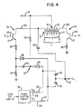
- Fig. 4 there is shown a schematic circuit diagram of the line driver 29, pulse transformer 31 and the preferred embodiment of the adjustment circuit 35.
- the modified pulse shaping circuit 25 can now include a shift register, a buffer, a resistor ladder network, an analog filter and a phase shifting circuit (not shown) to develop two analog phase-shaped, transmit signals (shown in Fig. 4 as V; and - V i ) that are 180 degrees out of phase with each other.
- the line 27 in Fig. 3 is split into two physical lines shown in Fig. 4 as 27A and 27B. These lines 27A and 27B are respectively driven in antiphase by the outputs V; and - V; of the modified circuit 25.
- the modified integrator 39 further includes a phase shifting circuit 58 coupled to the output of the digitalto-analog converter 57 for developing two analog control signals (shown in Fig. 4 as V C1 and V C2 ) that are 180 degrees out of phase with each other.
- the line 37 in Fig. 3 is split into two physical lines shown in Fig. 4 as 37A and 37B.
- the line 33 in Fig. 3 is also split into two physical lines shown in Fig. 4 as 33A and 33B.
- the signal V; on line 27A and the signal - V; on line 27B are respectively applied to the bases of NPN medium power transistors 71 and 73 whose collectors are respectively coupled via lines 33A and 33B to opposite ends of a winding 75 of the pulse transformer 31.
- the other winding 77 of the pulse transformer 31 is coupled via an associated tap 13 to the transmission line 11.
- the emitter of transistor 71 is coupled through serially-connected resistors 85 and 87 to ground, while the emitter of transistor 73 is coupled through resistor 89 to ground.
- Power for the transistors 71 and 73 is supplied from a + 5 volt source 79 to a center tap 83 of the winding 75.
- the preferred adjustment circuit 35 includes a pair of oppositely poled varactors or varactor diodes 91 and 93.
- Varactor 91 has its anode connected to the junction of resistors 85 and 87 and its cathode coupled via a capacitor 95 to an output terminal 97.
- a capacitor 99 is connected between the line 33A and the output terminal 97.
- varactor 93 has its anode coupled via a capacitor 101 to the output terminal 97 and its cathode coupled via a capacitor 103 to the junction of resistors 85 and 87.
- a resistor 105 is connected between the + 5 volt source 79 and the junction of the varactor 93 and capacitor 103.
- control signals V c1 and V c2 from the previously discussed, modified version of integrator 39 are respectively applied over lines 37A and 37B to the preferred adjustment circuit 35 shown in Fig. 4. It will be recalled that the control signals V c1 and V c2 are 180 degrees out of phase with each other.
- Control signal V c1 is applied from line 37A through a resistor 107 to the cathode of varactor 91 to control the capacitance of varactor 91.
- control signal V c2 is applied from line 37B through a resistor 109 to the anode of varactor 93 to control the capacitance of varactor 93.
- the output signal from the adjustment circuit 35 of Fig. 4 is provided at the output terminal 97 and is designated as V u .
- V cc represents the D.C. voltage of a power supply (not shown)
- Z L represents the impedance of the transmission line 11
- a voltage source V r connected in series between V cc and Z L represents a voltage transmitted from a remote station and induced into the winding 77 of the pulse transformer 13 (Fig 4)
- T represents the transistor 71 (Fig. 4)
- Re represents the resistors 85 and 87 (Fig. 4).
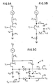
- Fig. 5A is a simplified representation of that portion of Fig. 4 which includes the transmission line 11 and the pulse transformer 31 being driven by the two medium power transistors 71 and 73.
- Fig. 5A will now be discussed in transmit, receive and collision modes of operation.
- the line driver 29 (Figs. 3 and 4) operates as a normal transistor amplifier T, of which the emitter impedance is equal to R e and the collector impedance is equal to Z L' the line impedance.
- the voltage generated on the collector of transistor T thus is: where:
- the leakage inductance of the pulse transformer 31 may be neglected.
- the collector voltage is:
- the impedance at the collector of T 1 will now be further analyzed. Because the associated tap 13 (Fig. 3) is connected to a point somewhere on the transmission line 11 (Fig. 3) and is not the end of the transmission line 11, the impedance with which the transceiver 15 (Figs. 2 and 3) is loaded consists of two transmission line impedances in parallel for an impedance of Z L /2. However, the line driver 29 includes two balanced, current source drivers or transistors 71 and 73 (Fig. 4). Each of the transistors 71 and 73 provides the current required for one direction of the transmission line 11. So the impedance at the collector of transistor T 1 is equal to Z L' Thus the voltage V c on the collector of T 1 is:
- Fig. 5B shows a modification of the circuit of Fig. 5A by the addition of serially connected capacitors C1 and C2 coupled across the collector-emitter region of the transistor T 1 .
- Capacitors C1 and C2 represent the subtractor 43 of Fig. 3.
- the signal at the collector of T 1 appears at the output as a component of the output signal V u and is attenuated by a factor determined by the ratio of the capacitances of C1 and C2. It will be recalled that during a collision the sum of the local transmitted signal and the received signal V r is present on the collector of T 1 as V c . Also the emitter signal V e of T 1 appears at the output as another component of V u and is also attenuated by a factor determined by the ratio of the capacitances of C1 and C2. Because the signal V e is 180 degrees out of phase with the transmitted signal at the collectot of T 1 , the crosstalk signal is cancelled and only the received signal V r remains in the output signal V u of the adjustment circuit 35.
- V u of the adjustment circuit 35 is given by: where V is the signal voltage at the collector of T, and V e is the signal voltage at the emitter of T l .
- Equation (6) can be rewritten as:
- the crosstalk signal is cancelled and only the receive signal Vr, attenuated by a factor a, remains in the output signal V u .
- Equation (9) only four different components appear, namely C1, C2, R e and Z L .
- the first three (C1, C2 and R e ) can be selected with a high degree of accuracy, but the line impedance Z L of the transmission line 11 (Fig. 1) may vary over a wide range of, for example, 70 to 110 ohms.
- the hybrid adjustment of the adjustment circuit 35 for these impedances can be achieved by adjusting either or both of the capacitors C1 and C2.
- a preferred form of a variable capacitor is the well-known varactor or varactor diode.
- the capacitance of a varactor can be readily adjusted by varying the D.C. voltage across the varactor. It will be recalled that, in the preferred embodiment of the adjustment circuit 35 in Fig. 4, two varactors 91 and 93 were used and that these were oppositely poled varactors which were respectively driven by two control signals V C1 and V C2 that were 180 degrees out of phase with each other.
- Such an arrangement of varactors has the following advantages.
- Fig. 5C there is shown a simplified modification of the circuit of Fig. 5B to provide an adjustment circuit 35 which can be automatically adjusted by varying the control signals V C1 and V C2'
- cl in Figs. 5B and 5C is the same as capacitor 99 in Fig. 4 and that capacitor C2 in Fig. 5B has been replaced in Fig. 5C with the varactors 91 and 93, capacitors 95 and 101, resistors 105, 107 and 109, and output terminal 97 (found in Fig. 4) to form the adjustment circuit 35 shown in Fig. 4.
- a circuit is implemented to automatically vary the control voltages V C1 and V C2 of the varactors 91 and 93 such that the crosstalk introduced from the line 33 of Fig. 1 or lines 33A and 33B of Fig. 4 to the output terminal 97 is minimized.
- the control voltages V C1 on line 37A and V C2 on line 37B for the varactors 91 and 93, respectively, are derived from the integrator 39 (Fig. 3).
- the integrator 39 is implemented with a digital counter 55, a digital-to-analog converter 57 and further includes a phase shifting circuit (not shown) for developing the opposite phase control signals V C1 and V c2 . If, in equation (10), the capacitance C2 is too large, the transmit signal V; and the output signal V u have the same polarity.
- the capacitance C2 (or the capacitances of the varactors 91 and 93 that replace C2) must be decreased and the control voltages V C1 and V C2 for the varactors 91 and 93 must both be increased (since the capacitance of a varactor is inversely proportional to the control voltage).
- V C1 is increasing in amplitude in one polarity
- V C2 is increasing in amplitude in the opposite polarity, and vice versa, since they have opposite polarities. As shown in Fig.
- the voltage across the varactor 91 increases because the anode of varactor 91 is connected to ground via the resistor 87 while the increasing V C1 voltage is applied to the cathode of varactor 91; and, similarly, the voltage across the varactor 93 increases because the cathode of varactor 93 is connected to the + 5 volt source 79 via the resistor 105 while the decreasing V C2 voltage is applied to the anode of varactor 93.
- the voltage across both of the varactors 91 and 93 increases.
- the control voltage V C1 increases if the count of the up/down counter 55 is decreased.
- the transmit signal V; and the output signal V u have the same logical states, the counter 55 must count down.
- This operation is implemented in Fig. 3 by comparing the digitized forms of V u and V; in the EXCLUSIVE-OR gate 49. If V u and V; have the same logical states, the EXCLUSIVE-OR gate 49 applies a 0 state signal to the counter 55, and vice versa.
- a 0 state output of the gate 49 causes the counter 55 to decrement its count while a 1 state output of the gate 49 causes the counter 55 to increment its count. It will be appreciated that this causes the correlation between the signals V; and V u to be reduced towards zero.
- the function of the adjustment circuit 35 is to enable the detection of a received signal from a remote station while the local station 9 itself is transmitting. This function can only be performed when the adjustment circuit 35 is properly adjusted for crosstalk cancellation and is also in a stable condition. Under these conditions the transmit signal is subtracted from the composite signal (sum of the transmitted and received signals) on the line 33 of Fig. 1 or line 33A of Fig. 4 so that only the receive signal remains at the V u output 97 of the adjustment circuit 35.
- Adjusting of the adjustment circuit 35 is performed on the first transmission of the station. However, after the initial power-up of the local station 9, the adjustment circuit 35 is not properly adjusted. As a consequence, crosstalk will result at the output of the adjustment circuit 35, causing the level detector circuit 51 (Fig. 3) to develop an erroneous carrier/collision signal. Normally, since the station 9 is transmitting, the station controller 17 (Fig. 2) would interpret this carrier/collision signal as a collision. However, after initial powerup the adjustment circuit 35 needs some time to be adaptively adjusted. To avoid such an erroneous collision after initial power-up, the controller 17 (Fig. 2) ignores the collision signal during, for example, the first 128 bits of a transmission when the adaptive hybrid 23 (Fig.
- the adjustment of the adjustment circuit 35 will not be completed within the exemplary first 128 bits of transmission after initial power-up. After that exemplary 128 bit training period, there will still be a significant signal present at the output of the adjustment circuit 35, which signal will be detected by the level detector circuit 51 as a carrier/collision signal. In this case, the station controller 17 (Fig. 2) will interpret the carrier/collision signal as a collision, abort the transmission and re-try another transmission after a random time period.
- the adaptive hybrid 23 then operates in its normal operation mode. In this normal operation mode the output of the adjustment circuit 35 will always be below the detection level of the level detector circuit 51 (Fig. 3), except in the case of noise on the line 11 when data is also being received.
- the adaptive hybrid 23 will continue to adaptively adjust itself to compensate for any changes in component values in the adaptive hybrid 23 and any change in the impedance of the transmission line 11 (Figs. 1 through 4) due to temperature changes or other effects.
- the output signal from the adjustment circuit 35 is either a noise spike of a received signal transmitted from a remote station. If the signal from the adjustment circuit 35 is of sufficient amplitude and duration, the signal will be passed by amplifier 45, detected as a carrier/collision signal by the detector circuit 51 (Fig. 3) and interpreted by the station controller 17 (Fig. 2) as a carrier detect. In this case normal data reception begins.
- the controller 17 removes the adjust enable signal to the up/down counter 55 in integrator 39 (Fig. 3).
- the counter 55 hhen stops counting, thereby preventing an undesirable adjustment of the adjustment circuit 35 during a collision. In such a collision, as stated before, the transmission from station 9 is aborted.
- the adjustment of the adjustment circuit 35 occurs when only local station 9 is transmitting.
- the adaptive hybrid 23 is latched and remains in a fixed position when the adjust enable signal is removed from the counter 55 in the integrator 39 (Fig. 3).
- the adjust enable signal from the controller 17 Fig. 2 enables the counter 55 to count, thereby enabling the adaptive hybrid 23 to adaptively adjust itself to minimize any crosstalk at the output of the adjustment circuit 35.
- the invention thus provides a system and method for minimizing the crosstalk from a transmitter to a receiver by adaptively forcing to zero the correlation between the output of the transmitter and the output of an adaptive hybrid coupled between the transmitter and receiver.
Landscapes
- Engineering & Computer Science (AREA)
- Physics & Mathematics (AREA)
- Computer Networks & Wireless Communication (AREA)
- Signal Processing (AREA)
- Mathematical Physics (AREA)
- Theoretical Computer Science (AREA)
- Power Engineering (AREA)
- Software Systems (AREA)
- Computer Hardware Design (AREA)
- General Physics & Mathematics (AREA)
- Cable Transmission Systems, Equalization Of Radio And Reduction Of Echo (AREA)
Abstract
Description
- This invention relates to adaptive hybrid circuits of the kind coupled to signal transmit means, and to signal receive means of a local station coupled to a signal transmission line, for adaptively minimizing crosstalk from said transmit means to said receive means including comparison means adapted to generate an adjustment control signal and adjustment means adapted to modify a signal from said transmission line in dependence on said adjustment control signal and in dependence on said transmit signal, to provide a modified signal to said receive means representative of only the received signal component, whereby said comparison means and said adjustment means are effective in operation to reduce towards zero the correlation between said output signal from said receive means and said transmit signal, and wherein said compararison means includes an EXCLUSIVE-OR gate and an integrator circuit, with said EXCLUSIVE-OR gate having an output coupled to said integrator circuit.
- The invention has a particular application to a tramsmission system where the transmitter and receiver are coupled to a two-wire transmission line or communication channel, such as a coaxial or twisted pair cable, of a local area network including a plurality of transmitter/receiver stations coupled to the same two-wire communication channel.
- In the transmitter/receiver circuitry of a bus-type local area network based on CSMA/CD (carrier sense multiple access with collision detection), a hybrid circuit can be used for the separation or isolation of simultaneously transmitted and received signals at one of the stations in the network. This separation allows the implementation of collision detection at larger transmit to receive level ratios than without a hybrid. Thus, larger transmission distances can be achieved by using a hybrid. A hybrid may be designed for a fixed nominal transmission line impedance. This means that the maximum attenuation of the transmitted signal crosstalk into the recived signal is obtained for only one transmission line impedance. In addition, the crosstalk attenuation for a given transmission line impedance will depend on the tolerances of the components utilized in the hybrid. Thus, any change in the impedance of the transmission line or in the values of the components in the hybrid, such as due to a temperature change, can prevent the hybrid from optimally cancelling the transmitted signal crosstalk from the received signal.
- An adaptive hybrid circuit is known from US-A-3 810 182. The known adaptive hybrid circuit is interposed between the transmitter and the receiver at one end of a transmission channel interconnecting a local station and a remote station. The output signal from the transmitter and the signal on the transmission channel are applied to a summer device operative as a subtractor, the output signal of the summer device being applied, together with the transmitter output signal, to respective gain and phase correlator circuits. The output signal on the transmitter is also applied via sequentially connected variable phase shift and variable gain circuits to the transmission channel, the variable phase shift circuit and variable gain circuits being controlled by respective output signals from the gain and phase correlator circuits. This arrangement is effective to filter out the transmitter signal component at the local station such that only the receive signal component from the transmission channel is passed to the receiver at the local station. This known adaptive hybrid circuit utilizes separate gain and phase control circuits and has the disadvantage of being complex in construction and hence expensive to manufacture.
- An adaptive hybrid circuit of the kind specified is known from IBM Technical Disclosure Bulletin, Vol. 26, No. 8, January, 1981, pages 3788 - 3790. This known adaptive hybrid circuit operates as an echo suppressor for telephone circuits employing full-duplex communication over a low-speed point-to-point telephone line. The transmitted signal is applied to a controllable gain amplifier and to an echo correlation detector which also receives an output derived from a subtractor having inputs connected to the output of the controllable gain amplifier and to the transmission line. The output of the echo correlation detector controls the controllable gain amplifier such that the transmitted signal is cancelled from the received signal. The echo correlation detector includes an EXCLUSIVE-OR gate having an output which controls the operation of a low-pass filter which provides the control signal for the controllable gain amplifier.
- US-A-3 973 089 discloses an adaptive hybrid circuit for use in telephone systems wherein the transmit, receive and two-wire ports are isolated from each other by transformers: Cross-talk cancellation is effected by utilizing an impedance synthesis network including a tapped delay line, and controlled by a correlation control loop which controls the tap weights of the tapped delay line.
- FR-A-2 485 842 discloses apparatus for transmitting and receiving data over a full-duplex transmission channel. The apparatus includes a two wire-four wire interface circuit, including an adaptive balancing network, and a digital echo cancelling circuit. Both the interface circuit and the echo cancelling circuit contribute to the reduction of the undesired effect of echo signals. The echo cancelling circuit includes an adaptive digital filter which synthesizes the echo signal and has an output coupled via a digital-to-anolog convertor to a subtractor circuit. The interface circuit operates in the manner of a Wheatstone bridge circuit including fixed resistors, an adjustable balancing network, and the input impedance of the primary winding of the isolating transformer. The adjustable balancing network is controlled by a feedback control circuit. The feedback control circuit includes a rectifier and filter, a sampler and a comparator which controls the operation of a bistable circuit. The output of the bistable circuit controls the counting direction of an up/down counter, outputs from which are connected to switches connected across resistors in the balancing network. A control signal ensures that the up/down counter is operative only during a period of a few dozen milliseconds when a control signal is transmitted.
- Acording to the present invention, there is provided an adaptive hybrid circuit of the kind specified, characterized in that said EXCLUSIVE-OR gate is adapted to compare an output signal from said receive means with a transmit signal to be transmitted by said transmit means, and in that said integrator circuit includes an up/down counter enabled only during transmission of a signal by said transmit means to count up or down in dependence on the output signal from said EXCLUSIVE-OR gate, said up/down counter being coupled to a digital-to-analog converter adapted to provide said adjustment control signal.
- It will be appreciated that an adaptive hybrid circuit according to the invention is of simple construction and hence relatively inexpensive to manufacture. Another advantage is that the adaptive hybrid circuit is suitable for use in an implementation in which a bus system network utilizes high speed data transmission rates of up to 1 Megabit per second.
- In a preferred embodiment of the invention an adaptive hybrid circuit is coupled between a transmitter and a receiver. The adaptive hybrid circuit includes a comparator, an integrator and an adjustment circuit. The output from the receiver is compared in the comparator with a transmit signal to develop a first signal which causes the integrator to develop a second signal having an amplitude which varies as a function of the state of the first signal. The transmit signal, the second signal and a composite signal comprised of the received signal and a crosstalk signal from the transmitter are applied to the adjustment circuit. In the adjustment circuit, the transmitted signal is multiplied by the second signal to develop a crosstalk cancelling signal which varies automatically to cancel the crosstalk signal in the composite signal for any given transmission line impedance. When the crosstalk is cancelled, the output of the adjustment circuit only contains the received signal which is detected by the receiver.
- One embodiment of the present invention will now be described by way of example with reference to the accompanying drawings, in which:
- Fig. 1 is a schematic block diagram of a plurality of communications stations individually coupled to a common transmission medium to form a local area network;
- Fig. 2 is a schematic block diagram of a typical station in the local area network;
- Fig. 3 is a schematic block diagram of a transceiver in the station of Fig. 2, which transceiver includes a transmitter, a receiver and an adaptive hybrid circuit coupled between the transmitter and receiver;
- Fig. 4 is a schematic diagram of the
line driver 29,pulse transformer 31, an additional part of theintegrator 39 and a preferred embodiment of theadjustment circuit 35 of Fig. 3; and - Figs. 5A, 5B and 5C are simplified circuits useful for explaining the operation of the preferred embodiment of the
adjustment circuit 35 of Fig. 4. - Although the invention will be described in relation to its application in a local area network employing a serial bus, it should be realized that its application should not be restricted to such utilization.
- Referring now to Fig. 1, there is shown a communications network including a plurality of
stations stations 91, 92°o.9N is connected to the transmission line 11 by an associated two-wire connection or tap 13 for transmitting data into the transmission line 11 as well as receiving data from the transmission line 11. The communications network forms a local area network (LAN) utilizing the well-known CSMA/CD (carrier sense multiple access with collision detection) protocol. Briefly, if a station detects no activity on the transmission line 11, then the station may start transmitting. If two stations start transmitting simultaneously or substantially simultaneously, then a "collision" occurs. This collision is detected by both stations and they will both abort transmission and re-try transmission after a random time period. - Referring to Fig. 2, there is shown a block diagram of a
typical station 9. Thestation 9 includes atransceiver 15 which is coupled to astation controller 17. Thetransceiver 15 includes atransmitter 19, areceiver 21 and anadaptive hybrid circuit 23. - In operation, a "transmit signal" comprised of data to be transmitted is applied from the
controller 17 to thetransmitter 19 for signal processing and transmission onto the transmission line 11 by way of the associatedtap 13. Signals received from the transmission line 11 are applied via thetap 13 andadaptive hybrid 23 to thereceiver 21 for detection. A detected "receive signal" is applied from thereceiver 21 to thecontroller 17 for subsequent utilization by thecontroller 17. Bi-directional control signals are selectively utilized by thetransceiver 15 andstation controller 17 for proper timing and control operations. As will be explained later, theadaptive hybrid 23 minimizes the crosstalk from thetransmitter 19 to thereceiver 21 so that a signal on the transmission line 11 from a remote station can be detected while thestation 9 is transmitting. A detailed description of thestation controller 17 is unnecessary for an understanding of the present invention. - Referring now to Fig. 3, there is shown a block diagram of the
transceiver 15. A transmit signal comprised of Manchester coded data to be transmitted is supplied at a rate of one megabit (1 Mbit) per second from the controller 17 (Fig. 2) to apulse shaping circuit 25. Thepulse shaping circuit 25 smooths the sharp transitions in the Manchester coded transmit signal to suppress harmonics in that transmit signal. In addition, thepulse shaping circuit 25 also provides pre-emphasis to the transmit signal to compensate for part of the subsequent distortion of that transmit signal which is introduced by the transmission line 11. In an exemplary implementation thepulse shaping circuit 25 can include a shift register, a buffer, a resistor ladder network and an analog filter. However, it should be understood that thepulse shaping circuih 25 can be implemented differently and since the details of thepulse shaping circuit 25 are not essential to an understanding of the present invention, the pulee shaping circuit not be further described. - The output of the
pulse shaping circuit 25 is applied via aline 27 to aline driver 29, which together with thepulse shaping circuit 25 may comprise thetransmitter 19. Theline driver 29 includes two transistors (Fig. 5) which are used as current sources and are driven in antiphase (180 degrees out of phase with each other), as will be explained later. - The
transmitter 19, as well as the receiver 21 (via the adaptive hybrid 23), are coupled to the transmission line 11 viatap 13 by means of apulse transformer 31. Thetransformer 31 provides the common mode rejection for thereceiver 21 and the ground isolation to avoid current (A.C. mains) problems. - In operation, the output of the
line driver 29 is applied by way of aline 33 to drive thepulse transformer 31. When so driven, thepulse transformer 31 feeds the output transmit signal from thetransmitter 19 onto the transmission line 11 via the associatedtap 13. However, in certain environments thepulse transformer 31 may be omitted. - As indicated in Fig. 3, any signal transmitted onto the transmission line 11 from a remote station is received from the transmission line 11 via the
tap 13 andtransformer 31. As a result, theline 33 can carry a composite signal formed by the output signal from theline driver 29 together with any signal which may be received from the transmission line 11 via thetap 13 andpulse transformer 31. - The
line 27 from the output of thepulse shaping circuit 25,line 33 from the output of theline driver 29 and aline 37 from the output of anintegrator 39 are all connected to anadjustment circuit 35. In the embodiment of theadjustment circuit 35 that is shown in Fig. 3, theadjustment circuit 35 includes amultiplier 41 and a combiner orsubtractor 43. A pulse shaped transmit signal on theline 27 and the signal on theline 37 are multiplied together in themultiplier 41 to adaptively develop a product signal which is an estimate of the crosstalk (from the transmitter 19) that may be contained in the composite signal on theline 33. As will be explained later in more detail, this crosstalk estimate is subtracted in the subtractor 43 from a composite signal on theline 33 to cancel out the crosstalk (from the transmitter 19) that may be contained in that composite signal. The difference signal at the output of thesubtractor 43 is the output of theadjustment circuit 35. Thus, only a received signal from the transmission line is adaptively developed at the output of theadjustment circuit 35. - In the embodiment of the invention (as shown in Fig. 3), the
adjustment circuit 35 includes a physically separatestandard multiplier circuit 41 and a standard adder/subtractor orcombiner circuit 43 functioning as a subtractor. However, in the preferred embodiment of the invention, the adjustment circuit 35 (as shown in Fig. 5) does not include a physically separate multiplier and subtractor. - The output of the
adjustment circuit 35 is applied to thereceiver 21 which comprises anamplifier 45 and apulse shaping circuit 47. Theamplifier 45 has a high input impedance to minimize the loading of the transmission line 11. In addition, theamplifier 45 preferably includes filter characteristics to compensate for part of the distortion of the received signal that is generated by the transmission line 11. The design of such anamplifier 45 is well-known by those skilled in the art and, therefore, no further description of theamplifier 45 is needed. - The output of the
amplifier 45 is applied to thepulse shaping circuit 47 which may include a standard high speed comparator to digitize the output of theamplifier 45 to develop a digital "receive signal". This receive signal, which is the output of thereceiver 21, is applied to digital circuits (not shown) in the station controller 17 (Fig. 2) for subsequent processing and also applied to an EXCLUSIVE-OR (EX-OR) gate 49 (to be discussed). - The output of the
amplifier 45 is also applied to alevel detector circuit 51. Thislevel detector circuit 51 is implemented to develop a carrier/collision signal when it detects the presence of any signal above a predetermined threshold level. Such a carrier/collision signal indicates the detection of a transmission from a remote station on the transmission line 11. This carrier/collision signal is applied to thestation controller 17. Since thecontroller 17 knows when it is transmitting a transmit signal, it interprets the carrier/collision signal as the detection of a collision when it is transmitting the transmit signal and as the detection of cartier when it is not transmitting the transmit signal. - As stated before the digital receive signal output of the
pulse shaping circuit 47 is applied to an EXCLUSIVE-OR (EX-OR)gate 49. The digital transmit signal from thecontroller 17 is also applied to thegate 49 via adelay 53.Delay 53 compensates for circuit delays in theadaptive hybrid circuit 23 andreceiver 21. The EXCLUSIVE-OR gate 49 functions as a digital comparator by comparing its input digital transmit and receive signals with each other. When the transmit and receive signals have the same logical states, thegate 49 develops a 0 state output. Similarly, when the transmit and receive signals have different logical states, thegate 49 develops a 1 state output. - The output of the EXCLUSIVE-
OR gate 49 is applied to theintegrator 39. The EXCLUSIVE-OR gate 49,integrator 39 andadjustment circuit 35 essentially comprise theadaptive hybrid circuit 23 of Fig. 2. Theadaptive hybrid 23 andreceiver 21 form a loop for adaptively cancelling out any transmitter crosstalk from the output of the adjustment circuit 35 (input to the receiver 21). - The
integrator 39 includes a digital up/downcounter 55 and a digital-to-analog converter (D/A CONV.) 57. Thecounter 55 is initially preset to a predetermined count by a preset signal from thecontroller 17. Clock pulses from aclock generator 59 are applied to thecontroller 17 to control the transmit clock rate of the transmit signal and are also applied to the count input of thecounter 55. During any period of time that thecontroller 17 generates a transmit signal, thecontroller 17 also applies an adjust enable signal to thecounter 55 to enable thecounter 55 to count clock pulses during that transmission. When enabled by the adjust enable signal, the up/down counter 55 counts up or down as a function of the logical state of the up/down signal from the EXCLUSIVE-OR gate 49. For example, when the transmit and receive signals to thegate 49 have the same logical states, the 0 state output of thegate 49 forces thecounter 55 to count clock pulses by decrementing its count. Conversely, when the transmit and receive signals to thegate 49 have different logical states, the 1 state output of thegate 49 forces thecounter 55 to count clock pulses by incrementing its count. Outputs from the stages (not shown) of thecounter 55 are applied to the digitalto-analog converter 57 which may be formed by a resistor ladder network (not shown). The digital-to-analog converter 57 converts the digital count from thecounter 55 to an analog signal which is representative of the digital count in thecounter 55. - It will be appreciated that an advantage of utilizing a
digital counter 55 in theintegrator 39 is that the count of thecounter 55 does not change between transmissions. - The analog signal from the
converter 57 is applied overline 37 to theadjustment circuit 35. The signal on theline 37 operates as a multiplication factor for the pulse shaped transmit signal online 27 to enable themultiplier 41 to develop the crosstalk estimate which, as stated before, is subtracted in the subtractor 43 from the composite signal online 33 to adaptively develop a residual received signal. However, as stated before, in the preferred embodiment of the adjustment circuit 35 (Fig. 4) themultiplier 41 andsubtractor 43 are effectively combined. - Although not essential to an understanding of the present invention, it is deemed helpful to provide a brief description of the underlying theory. For ease of understanding, this theory will be presented in the form of an algorithm described on a signal sample basis, although the actual implementation in the circuit shown in Fig. 3 is in the form of continuous signals on the
lines subtractor 43. - Thus, the composite signal on the
line 33, which is regarded as being sampled at the symbol rate, can be represented as:
- Sk = composite signal on
line 33 - bk = received data symbols on
line 33 - ak = transmitted data symbols on
line 33, E Jak 2) = 1 - gk = intersymbol interference from line 11
- rk = echo path impulse response
- ro = bridge crosstalk
- Subtracting the crosstalk estimate from
multiplier 41 from the composite signal online 33 results in an error signal ek at the output of thesubtractor 43, where:
- ak = transmitted data symbols on
line 27 - Co = multiplication factor on
line 37 - It is clear that the choice Co = ro completely cancels the crosstalk and therefore is the optimum choice. Introducing the
error 00 = ro - co, one can write the mean square error as:
- Assuming mutually uncorrelated data symbols, the uncancellable mean square error is:

- A stochastic gradient algorithm can be used for adaptive adjustment of co.
- The gradient of the mean-square error is given by:

- Adjustments are most conveniently made by using averaged estimates according to the recursion:

- While the above algorithm was described on a sampled basis, it should be readily apparent to those skilled in the art that it can be implemented with the analog circuitry shown in Fig. 3.
- Referring now to Fig. 4, there is shown a schematic circuit diagram of the
line driver 29,pulse transformer 31 and the preferred embodiment of theadjustment circuit 35. - In utilizing a preferred embodiment of the
adjustment circuit 35, several modifications have to be made in thepulse shaping circuit 25,integrator 39 andlines pulse shaping circuit 25 can now include a shift register, a buffer, a resistor ladder network, an analog filter and a phase shifting circuit (not shown) to develop two analog phase-shaped, transmit signals (shown in Fig. 4 as V; and - Vi) that are 180 degrees out of phase with each other. Theline 27 in Fig. 3 is split into two physical lines shown in Fig. 4 as 27A and 27B. Theselines circuit 25. The modifiedintegrator 39 further includes aphase shifting circuit 58 coupled to the output of the digitalto-analog converter 57 for developing two analog control signals (shown in Fig. 4 as VC1 and VC2) that are 180 degrees out of phase with each other. Theline 37 in Fig. 3 is split into two physical lines shown in Fig. 4 as 37A and 37B. Finally, theline 33 in Fig. 3 is also split into two physical lines shown in Fig. 4 as 33A and 33B. - The signal V; on
line 27A and the signal - V; online 27B are respectively applied to the bases of NPNmedium power transistors lines pulse transformer 31. The other winding 77 of thepulse transformer 31 is coupled via an associatedtap 13 to the transmission line 11. The emitter oftransistor 71 is coupled through serially-connectedresistors transistor 73 is coupled throughresistor 89 to ground. Power for thetransistors volt source 79 to acenter tap 83 of the winding 75. - The
preferred adjustment circuit 35 includes a pair of oppositely poled varactors orvaractor diodes Varactor 91 has its anode connected to the junction ofresistors capacitor 95 to anoutput terminal 97. A capacitor 99 is connected between theline 33A and theoutput terminal 97. In a similar manner,varactor 93 has its anode coupled via acapacitor 101 to theoutput terminal 97 and its cathode coupled via acapacitor 103 to the junction ofresistors resistor 105 is connected between the + 5volt source 79 and the junction of thevaractor 93 andcapacitor 103. - The control signals Vc1 and Vc2 from the previously discussed, modified version of
integrator 39 are respectively applied overlines preferred adjustment circuit 35 shown in Fig. 4. It will be recalled that the control signals Vc1 and Vc2 are 180 degrees out of phase with each other. Control signal Vc1 is applied fromline 37A through aresistor 107 to the cathode ofvaractor 91 to control the capacitance ofvaractor 91. Similarly, control signal Vc2 is applied fromline 37B through aresistor 109 to the anode ofvaractor 93 to control the capacitance ofvaractor 93. The output signal from theadjustment circuit 35 of Fig. 4 is provided at theoutput terminal 97 and is designated as Vu. - Referring to Figs. 5A, 5B and 5C, the operation of the
adjustment circuit 35 will now be explained. In each of the Figs. 5A, 5B and 5C, Vcc represents the D.C. voltage of a power supply (not shown), ZL represents the impedance of the transmission line 11, a voltage source Vr connected in series between Vcc and ZL represents a voltage transmitted from a remote station and induced into the winding 77 of the pulse transformer 13 (Fig 4), T, represents the transistor 71 (Fig. 4) and Re represents theresistors 85 and 87 (Fig. 4). Furthermore, it should be noted that in the analysis of the operation of each of the circuits of Figs. 5A, 5B and 5C only A.C. voltages will be considered. - Fig. 5A is a simplified representation of that portion of Fig. 4 which includes the transmission line 11 and the
pulse transformer 31 being driven by the twomedium power transistors - When the
station 9 is transmitting, the line driver 29 (Figs. 3 and 4) operates as a normal transistor amplifier T, of which the emitter impedance is equal to Re and the collector impedance is equal to ZL' the line impedance. The voltage generated on the collector of transistor T, thus is:
- V; = the pulse shaped transmit signal from
pulse shaping circuit 25 - LL = the leakage inductance of
pulse transformer 31 - w=ω=2πf
- j = a 90 degree phase shift in the inductive reactance (wLL)
- For an analysis of the operation of the circuit of Fig. 5A, the leakage inductance of the
pulse transformer 31 may be neglected. In this case the collector voltage is:
- The impedance at the collector of T1 will now be further analyzed. Because the associated tap 13 (Fig. 3) is connected to a point somewhere on the transmission line 11 (Fig. 3) and is not the end of the transmission line 11, the impedance with which the transceiver 15 (Figs. 2 and 3) is loaded consists of two transmission line impedances in parallel for an impedance of ZL/2. However, the
line driver 29 includes two balanced, current source drivers ortransistors 71 and 73 (Fig. 4). Each of thetransistors 
- When the
station 9 is neither transmitting nor receiving, V; = 0 and therefore Vc = 0. However, when thestation 9 is not transmitting but is receiving from the transmission line 11 a signal Vr transmitted from a remote station, this received signal Vr will appear unattenuated at the collector of T1 because of the very high impedance of this type of circuit. Thus, in this receive only operation the voltage Vc at the collector of T1 is:
- As stated before, when the
local station 9 and a remote station both start transmitting simultaneously or substantially simultaneously, a collision occurs. When a collision occurs, the sum of both the received remote station signal (Vr) and the transmission - -Z-V/Re
- Fig. 5B shows a modification of the circuit of Fig. 5A by the addition of serially connected capacitors C1 and C2 coupled across the collector-emitter region of the transistor T1. Capacitors C1 and C2 represent the
subtractor 43 of Fig. 3. The output signal Vu of the circuit of Fig. 5B, which is taken from the junction of capacitors C1 and C2, corresponds to the output signal from the adjustment circuit 35 (Figs. 3 and 4). - The signal at the collector of T1 appears at the output as a component of the output signal Vu and is attenuated by a factor determined by the ratio of the capacitances of C1 and C2. It will be recalled that during a collision the sum of the local transmitted signal and the received signal Vr is present on the collector of T1 as Vc. Also the emitter signal Ve of T1 appears at the output as another component of Vu and is also attenuated by a factor determined by the ratio of the capacitances of C1 and C2. Because the signal Ve is 180 degrees out of phase with the transmitted signal at the collectot of T1, the crosstalk signal is cancelled and only the received signal Vr remains in the output signal Vu of the
adjustment circuit 35. - The cancellation of the crosstalk will now be explained mathematically. The output signal Vu of the
adjustment circuit 35 is given by:
- Equation (6) can be rewritten as:

- Substituting equation (5) into equation (6) and setting Ve = Vi results in:

- And if the following condition holds:


- Thus, with a correct choice of C1 and C2, the crosstalk signal is cancelled and only the receive signal Vr, attenuated by a factor a, remains in the output signal Vu.
- In equation (9) only four different components appear, namely C1, C2, Re and ZL. The first three (C1, C2 and Re) can be selected with a high degree of accuracy, but the line impedance ZL of the transmission line 11 (Fig. 1) may vary over a wide range of, for example, 70 to 110 ohms. The hybrid adjustment of the
adjustment circuit 35 for these impedances can be achieved by adjusting either or both of the capacitors C1 and C2. - In the preferred embodiment of the
adjustment circuit 35, only C2 is chosen to be adjusted because this minimizes the variation in load of the transmission line 11 (Fig. 1). A preferred form of a variable capacitor is the well-known varactor or varactor diode. The capacitance of a varactor can be readily adjusted by varying the D.C. voltage across the varactor. It will be recalled that, in the preferred embodiment of theadjustment circuit 35 in Fig. 4, twovaractors - 1. The capacitances of the varactors depends upon the voltages across them. This means that a large A.C. voltage on these varactors will result in a distorted signal due to the non-linear characteristics of the varactors. Using two varactors coupled together with opposite polarity (in antiparallel) results in distortion in both varactors having opposite polarity such that the distortion is almost completely eliminated.
- 2. Changing the control voltage of one of the varactors introduces noise in the received signal. The use of two varactors coupled together with opposite polarity and two control signals with opposite polarity has the advantage that the noise generated in the received signal by both control signals has an opposite polarity for both of the control signals and is therefore eliminated in the signal Vu at the output of the
adjustment circuit 35 - Referring now to Fig. 5C, there is shown a simplified modification of the circuit of Fig. 5B to provide an
adjustment circuit 35 which can be automatically adjusted by varying the control signals VC1 and VC2' Note that cl in Figs. 5B and 5C is the same as capacitor 99 in Fig. 4 and that capacitor C2 in Fig. 5B has been replaced in Fig. 5C with thevaractors capacitors resistors adjustment circuit 35 shown in Fig. 4. To automatically adjust theadjustment circuit 35 of Fig. 5C, a circuit is implemented to automatically vary the control voltages VC1 and VC2 of thevaractors line 33 of Fig. 1 orlines output terminal 97 is minimized. - Rewriting equation (8) results in:

- In equation (10) assume that the receive signal V, is zero (Vr = 0) and the transmit signal V; is non-zero. If the adjustment circuit 35 (Fig. 3) is unbalanced and no signal is received (Vr = 0), the polarity of the output signal Vu relative to V; indicates in what direction the capacitance C2 has to be adjusted to cancel out Vi from the signal Vu. If C2 is too large, Vu and V; have the same polarity. Otherwise, they have opposite polarities.
- The control voltages VC1 on
line 37A and VC2 online 37B for thevaractors integrator 39 is implemented with adigital counter 55, a digital-to-analog converter 57 and further includes a phase shifting circuit (not shown) for developing the opposite phase control signals VC1 and Vc2. If, in equation (10), the capacitance C2 is too large, the transmit signal V; and the output signal Vu have the same polarity. The capacitance C2 (or the capacitances of thevaractors varactors varactor 91 increases because the anode ofvaractor 91 is connected to ground via theresistor 87 while the increasing VC1 voltage is applied to the cathode ofvaractor 91; and, similarly, the voltage across thevaractor 93 increases because the cathode ofvaractor 93 is connected to the + 5volt source 79 via theresistor 105 while the decreasing VC2 voltage is applied to the anode ofvaractor 93. Thus, the voltage across both of thevaractors - The control voltage VC1 increases if the count of the up/down
counter 55 is decreased. Thus, if the transmit signal V; and the output signal Vu have the same logical states, thecounter 55 must count down. This operation is implemented in Fig. 3 by comparing the digitized forms of Vu and V; in the EXCLUSIVE-OR gate 49. If Vu and V; have the same logical states, the EXCLUSIVE-OR gate 49 applies a 0 state signal to thecounter 55, and vice versa. As stated before, a 0 state output of thegate 49 causes thecounter 55 to decrement its count while a 1 state output of thegate 49 causes thecounter 55 to increment its count. It will be appreciated that this causes the correlation between the signals V; and Vu to be reduced towards zero. - As described before, the function of the
adjustment circuit 35 is to enable the detection of a received signal from a remote station while thelocal station 9 itself is transmitting. This function can only be performed when theadjustment circuit 35 is properly adjusted for crosstalk cancellation and is also in a stable condition. Under these conditions the transmit signal is subtracted from the composite signal (sum of the transmitted and received signals) on theline 33 of Fig. 1 orline 33A of Fig. 4 so that only the receive signal remains at the Vu output 97 of theadjustment circuit 35. - Adjusting of the
adjustment circuit 35 is performed on the first transmission of the station. However, after the initial power-up of thelocal station 9, theadjustment circuit 35 is not properly adjusted. As a consequence, crosstalk will result at the output of theadjustment circuit 35, causing the level detector circuit 51 (Fig. 3) to develop an erroneous carrier/collision signal. Normally, since thestation 9 is transmitting, the station controller 17 (Fig. 2) would interpret this carrier/collision signal as a collision. However, after initial powerup theadjustment circuit 35 needs some time to be adaptively adjusted. To avoid such an erroneous collision after initial power-up, the controller 17 (Fig. 2) ignores the collision signal during, for example, the first 128 bits of a transmission when the adaptive hybrid 23 (Fig. 2) is in its training period or mode. If no remote station is transmitting onto the transmission line 11, the exemplary 128 bit training period will be sufficient for theadaptive hybrid 23 to adjust itself, as described before, so that the output of the adjustment circuit is substantially zero. In such a case the system of Fig. 3 will be in its normal operation and the Vr term in equation (10) is zero. - If another station is transmitting, then the adjustment of the
adjustment circuit 35 will not be completed within the exemplary first 128 bits of transmission after initial power-up. After that exemplary 128 bit training period, there will still be a significant signal present at the output of theadjustment circuit 35, which signal will be detected by thelevel detector circuit 51 as a carrier/collision signal. In this case, the station controller 17 (Fig. 2) will interpret the carrier/collision signal as a collision, abort the transmission and re-try another transmission after a random time period. - If the adjustment of the
adjustment circuit 35 during the initial training period is successful, theadaptive hybrid 23 then operates in its normal operation mode. In this normal operation mode the output of theadjustment circuit 35 will always be below the detection level of the level detector circuit 51 (Fig. 3), except in the case of noise on the line 11 when data is also being received. During each transmission of thelocal station 9, theadaptive hybrid 23 will continue to adaptively adjust itself to compensate for any changes in component values in theadaptive hybrid 23 and any change in the impedance of the transmission line 11 (Figs. 1 through 4) due to temperature changes or other effects. - If during normal operation the
adjustment circuit 35 develops an output signal, one of the following two situations has occurred. - If the
station 9 is not transmitting, then the output signal from theadjustment circuit 35 is either a noise spike of a received signal transmitted from a remote station. If the signal from theadjustment circuit 35 is of sufficient amplitude and duration, the signal will be passed byamplifier 45, detected as a carrier/collision signal by the detector circuit 51 (Fig. 3) and interpreted by the station controller 17 (Fig. 2) as a carrier detect. In this case normal data reception begins. - If the
station 9 is transmitting, then the output of theadjustment circuit 35 will subsequently cause thelevel detector circuit 51 to develop a carrier/collision signal which will be interpreted by thecontroller 17 as a collision. In this case, thecontroller 17 removes the adjust enable signal to the up/down counter 55 in integrator 39 (Fig. 3). Thecounter 55 hhen stops counting, thereby preventing an undesirable adjustment of theadjustment circuit 35 during a collision. In such a collision, as stated before, the transmission fromstation 9 is aborted. - Thus, as can be readily seen from the above-described operation, the adjustment of the
adjustment circuit 35 occurs when onlylocal station 9 is transmitting. Between two transmissions of thestation 9, theadaptive hybrid 23 is latched and remains in a fixed position when the adjust enable signal is removed from thecounter 55 in the integrator 39 (Fig. 3). Upon the next transmission during a non-collision mode, the adjust enable signal from the controller 17 (Fig. 2) enables thecounter 55 to count, thereby enabling theadaptive hybrid 23 to adaptively adjust itself to minimize any crosstalk at the output of theadjustment circuit 35. - The invention thus provides a system and method for minimizing the crosstalk from a transmitter to a receiver by adaptively forcing to zero the correlation between the output of the transmitter and the output of an adaptive hybrid coupled between the transmitter and receiver.
nk = noise samples, mean 0, variance 0-2.
of the
Claims (5)
Applications Claiming Priority (2)
| Application Number | Priority Date | Filing Date | Title |
|---|---|---|---|
| US06/623,302 US4715064A (en) | 1984-06-22 | 1984-06-22 | Adaptive hybrid circuit |
| US623302 | 1984-06-22 |
Publications (2)
| Publication Number | Publication Date |
|---|---|
| EP0187778A1 EP0187778A1 (en) | 1986-07-23 |
| EP0187778B1 true EP0187778B1 (en) | 1989-05-31 |
Family
ID=24497547
Family Applications (1)
| Application Number | Title | Priority Date | Filing Date |
|---|---|---|---|
| EP85903138A Expired EP0187778B1 (en) | 1984-06-22 | 1985-06-10 | Adaptive hybrid circuit |
Country Status (6)
| Country | Link |
|---|---|
| US (1) | US4715064A (en) |
| EP (1) | EP0187778B1 (en) |
| JP (1) | JPS61502510A (en) |
| CA (1) | CA1256526A (en) |
| DE (1) | DE3570817D1 (en) |
| WO (1) | WO1986000480A1 (en) |
Families Citing this family (36)
| Publication number | Priority date | Publication date | Assignee | Title |
|---|---|---|---|---|
| US4868874A (en) * | 1986-04-18 | 1989-09-19 | Hitachi, Ltd. | Echo canceller |
| US5119398A (en) * | 1988-05-12 | 1992-06-02 | Farallon Computing, Inc. | Signal regenerator for two-wire local area network |
| US5029203A (en) * | 1988-11-30 | 1991-07-02 | Rohm Co., Ltd. | Side tone preventive circuit for telephone |
| US5157697A (en) * | 1991-03-21 | 1992-10-20 | Novatel Communications, Ltd. | Receiver employing correlation technique for canceling cross-talk between in-phase and quadrature channels prior to decoding |
| US5511119A (en) * | 1993-02-10 | 1996-04-23 | Bell Communications Research, Inc. | Method and system for compensating for coupling between circuits of quaded cable in a telecommunication transmission system |
| US5528685A (en) * | 1994-07-08 | 1996-06-18 | At&T Corp. | Transformerless hybrid circuit |
| US6160790A (en) * | 1996-12-31 | 2000-12-12 | Paradyne Corporation | Crosstalk canceller system and method |
| US6169762B1 (en) | 1997-05-30 | 2001-01-02 | Lucent Technologies Inc. | Interface devices providing electrical isolation |
| US6205220B1 (en) * | 1998-06-29 | 2001-03-20 | Texas Instruments Incorporated | Method to mitigate the near-far fext problem |
| US7027537B1 (en) * | 1999-03-05 | 2006-04-11 | The Board Of Trustees Of The Leland Stanford Junior University | Iterative multi-user detection |
| US6614236B1 (en) | 1999-03-17 | 2003-09-02 | Cisco Technology, Inc. | Cable link integrity detector |
| US6970560B1 (en) | 1999-11-11 | 2005-11-29 | Tokyo Electron Limited | Method and apparatus for impairment diagnosis in communication systems |
| US6870901B1 (en) | 1999-11-11 | 2005-03-22 | Tokyo Electron Limited | Design and architecture of an impairment diagnosis system for use in communications systems |
| US6970415B1 (en) | 1999-11-11 | 2005-11-29 | Tokyo Electron Limited | Method and apparatus for characterization of disturbers in communication systems |
| US7864692B1 (en) | 1999-11-11 | 2011-01-04 | Tokyo Electron Limited | Method and apparatus for the prediction and optimization in impaired communication systems |
| US6978015B1 (en) | 1999-11-11 | 2005-12-20 | Tokyo Electron Limited | Method and apparatus for cooperative diagnosis of impairments and mitigation of disturbers in communication systems |
| US6834109B1 (en) * | 1999-11-11 | 2004-12-21 | Tokyo Electron Limited | Method and apparatus for mitigation of disturbers in communication systems |
| US20070047733A1 (en) * | 1999-12-15 | 2007-03-01 | Gordon Bremer | System and Method for Premises End Crosstalk Compensation |
| US6462688B1 (en) | 2000-12-18 | 2002-10-08 | Marvell International, Ltd. | Direct drive programmable high speed power digital-to-analog converter |
| US7194037B1 (en) | 2000-05-23 | 2007-03-20 | Marvell International Ltd. | Active replica transformer hybrid |
| US7312739B1 (en) | 2000-05-23 | 2007-12-25 | Marvell International Ltd. | Communication driver |
| USRE41831E1 (en) | 2000-05-23 | 2010-10-19 | Marvell International Ltd. | Class B driver |
| US6775529B1 (en) | 2000-07-31 | 2004-08-10 | Marvell International Ltd. | Active resistive summer for a transformer hybrid |
| US7433665B1 (en) | 2000-07-31 | 2008-10-07 | Marvell International Ltd. | Apparatus and method for converting single-ended signals to a differential signal, and transceiver employing same |
| US7095348B1 (en) | 2000-05-23 | 2006-08-22 | Marvell International Ltd. | Communication driver |
| US7113121B1 (en) | 2000-05-23 | 2006-09-26 | Marvell International Ltd. | Communication driver |
| US7606547B1 (en) | 2000-07-31 | 2009-10-20 | Marvell International Ltd. | Active resistance summer for a transformer hybrid |
| US7573839B2 (en) * | 2004-07-07 | 2009-08-11 | Broadcom Corporation | Line driver for an adaptive hybrid circuit |
| US7680226B2 (en) * | 2005-03-24 | 2010-03-16 | Dell Products L.P. | Minimizing dynamic crosstalk-induced jitter timing skew |
| US7312662B1 (en) | 2005-08-09 | 2007-12-25 | Marvell International Ltd. | Cascode gain boosting system and method for a transmitter |
| US7577892B1 (en) | 2005-08-25 | 2009-08-18 | Marvell International Ltd | High speed iterative decoder |
| US20080219389A1 (en) * | 2007-03-06 | 2008-09-11 | Sige Semiconductor Inc. | Feed-forward cancellation in wireless receivers |
| US20080219377A1 (en) * | 2007-03-06 | 2008-09-11 | Sige Semiconductor Inc. | Transmitter crosstalk cancellation in multi-standard wireless transceivers |
| ATE531139T1 (en) * | 2008-04-24 | 2011-11-15 | Alcatel Lucent | METHOD AND HYBRID CIRCUIT FOR NEAR CROSSTALK ATTENUATION IN BIDIRECTIONAL SIGNAL TRANSMISSION |
| US8125241B2 (en) * | 2009-10-07 | 2012-02-28 | Lsi Corporation | Automatic de-emphasis setting for driving capacitive backplane |
| US11855668B2 (en) * | 2022-05-19 | 2023-12-26 | Airoha Technology Corp. | 10BASE-T transmitter using waveform shaping for applying pre-compensation of inter-symbol interference and associated method |
Family Cites Families (14)
| Publication number | Priority date | Publication date | Assignee | Title |
|---|---|---|---|---|
| US3070309A (en) * | 1961-09-20 | 1962-12-25 | Phillips Petroleum Co | Voltage-sensitive capacitor bridge multiplier |
| DE1218007B (en) * | 1964-10-07 | 1966-06-02 | Telefunken Patent | Adjustable AC voltage amplifier |
| US3810182A (en) * | 1971-08-12 | 1974-05-07 | North American Rockwell | Adaptive electronic hybrid transformer |
| CA1006280A (en) * | 1973-10-29 | 1977-03-01 | General Electric Company | Adaptive hybrid circuit |
| US3973089A (en) * | 1973-10-29 | 1976-08-03 | General Electric Company | Adaptive hybrid circuit |
| US4087654A (en) * | 1975-11-28 | 1978-05-02 | Bell Telephone Laboratories, Incorporated | Echo canceller for two-wire full duplex data transmission |
| DE2921780C3 (en) * | 1979-05-29 | 1982-02-11 | Siemens AG, 1000 Berlin und 8000 München | Method and circuit arrangement for the transmission of data via a two-wire line |
| US4320498A (en) * | 1980-02-11 | 1982-03-16 | Apple Computer, Inc. | Auto balancing duplexer for communication lines |
| US4535206A (en) * | 1980-04-09 | 1985-08-13 | At&T Bell Laboratories | Echo cancellation in two-wire full-duplex data transmission with estimation of far-end data components |
| FR2485842B1 (en) * | 1980-06-30 | 1988-02-26 | Cit Alcatel | DEVICE FOR SEPARATING THE TRANSMISSION CHANNELS AND RECEIVING A DATA TRANSMISSION IN FULL DUPLEX |
| NL8100650A (en) * | 1981-02-11 | 1982-09-01 | Philips Nv | DEVICE FOR CORRECTING PULSE DISTORTION IN HOMOCHRONOUS DATA TRANSMISSION. |
| US4425483A (en) * | 1981-10-13 | 1984-01-10 | Northern Telecom Limited | Echo cancellation using transversal filters |
| FR2517905B1 (en) * | 1981-12-09 | 1985-11-29 | Telecommunications Sa | INITIALIZATION DEVICE FOR ECHO CANCELER AND ITS APPLICATION TO FAR ECHOES |
| US4610010A (en) * | 1984-12-10 | 1986-09-02 | Ncr Corporation | Control circuit for an adaptive hybrid control in a local area network |
-
1984
- 1984-06-22 US US06/623,302 patent/US4715064A/en not_active Expired - Lifetime
-
1985
- 1985-04-19 CA CA000479543A patent/CA1256526A/en not_active Expired
- 1985-06-10 EP EP85903138A patent/EP0187778B1/en not_active Expired
- 1985-06-10 DE DE8585903138T patent/DE3570817D1/en not_active Expired
- 1985-06-10 JP JP60502754A patent/JPS61502510A/en active Pending
- 1985-06-10 WO PCT/US1985/001085 patent/WO1986000480A1/en active IP Right Grant
Also Published As
| Publication number | Publication date |
|---|---|
| DE3570817D1 (en) | 1989-07-06 |
| WO1986000480A1 (en) | 1986-01-16 |
| JPS61502510A (en) | 1986-10-30 |
| EP0187778A1 (en) | 1986-07-23 |
| CA1256526A (en) | 1989-06-27 |
| US4715064A (en) | 1987-12-22 |
Similar Documents
| Publication | Publication Date | Title |
|---|---|---|
| EP0187778B1 (en) | Adaptive hybrid circuit | |
| US4539675A (en) | Echo canceller | |
| US5483551A (en) | Crosstalk suppression technique | |
| US5210774A (en) | Adaptive equalization system and method for equalizing a signal in a dce | |
| EP0145022B1 (en) | Method and apparatus for cancelling echo | |
| EP0577901B1 (en) | Adaptive equalization system and method | |
| JPS5923497B2 (en) | echo canceller | |
| JPS62128627A (en) | Data transmission apparatus | |
| US4587382A (en) | Echo canceller using end delay measurement | |
| USRE31253E (en) | Echo cancellation in two-wire, two-way data transmission systems | |
| JPS594336A (en) | Terminal unit in composite transmission system | |
| KR19990077047A (en) | Noise Impulse Impact Reduction Methods, Receivers, and Transmitters | |
| US4769808A (en) | Method of cancelling echoes in full-duplex data transmission system | |
| JP2591764B2 (en) | Adaptive time discrete filter | |
| US4613731A (en) | Method of cancelling listener echo in a digital data receiver, and device for implementing said method | |
| KR20060034204A (en) | Data transmission device and data transmission method | |
| EP0592747B1 (en) | Adaptive equalizing apparatus and method for token ring transmission systems using unshielded twisted pair cables | |
| US5297163A (en) | Method for processing signals for signal transmission in the base band | |
| EP0519498B1 (en) | Terminal apparatus for full-duplex data transmission having an echo canceller | |
| US4549048A (en) | Digital echo canceller | |
| US4593399A (en) | Method and apparatus for maximizing efficiency in satellite communications | |
| JP2928801B2 (en) | Echo cancellation method and subscriber line audio processing circuit | |
| US5084866A (en) | Transversal filter echo canceller | |
| US6934265B2 (en) | Interference cancellation receiver for high-speed communication systems | |
| JPH0473650B2 (en) |
Legal Events
| Date | Code | Title | Description |
|---|---|---|---|
| PUAI | Public reference made under article 153(3) epc to a published international application that has entered the european phase |
Free format text: ORIGINAL CODE: 0009012 |
|
| AK | Designated contracting states |
Kind code of ref document: A1 Designated state(s): DE FR GB |
|
| 17P | Request for examination filed |
Effective date: 19860628 |
|
| DET | De: translation of patent claims | ||
| 17Q | First examination report despatched |
Effective date: 19880316 |
|
| GRAA | (expected) grant |
Free format text: ORIGINAL CODE: 0009210 |
|
| AK | Designated contracting states |
Kind code of ref document: B1 Designated state(s): DE FR GB |
|
| REF | Corresponds to: |
Ref document number: 3570817 Country of ref document: DE Date of ref document: 19890706 |
|
| ET | Fr: translation filed | ||
| PLBE | No opposition filed within time limit |
Free format text: ORIGINAL CODE: 0009261 |
|
| STAA | Information on the status of an ep patent application or granted ep patent |
Free format text: STATUS: NO OPPOSITION FILED WITHIN TIME LIMIT |
|
| 26N | No opposition filed | ||
| REG | Reference to a national code |
Ref country code: GB Ref legal event code: 732E |
|
| REG | Reference to a national code |
Ref country code: FR Ref legal event code: TP |
|
| PGFP | Annual fee paid to national office [announced via postgrant information from national office to epo] |
Ref country code: FR Payment date: 19930330 Year of fee payment: 9 |
|
| PGFP | Annual fee paid to national office [announced via postgrant information from national office to epo] |
Ref country code: GB Payment date: 19930406 Year of fee payment: 9 |
|
| PGFP | Annual fee paid to national office [announced via postgrant information from national office to epo] |
Ref country code: DE Payment date: 19930624 Year of fee payment: 9 |
|
| PG25 | Lapsed in a contracting state [announced via postgrant information from national office to epo] |
Ref country code: GB Effective date: 19940610 |
|
| GBPC | Gb: european patent ceased through non-payment of renewal fee |
Effective date: 19940610 |
|
| PG25 | Lapsed in a contracting state [announced via postgrant information from national office to epo] |
Ref country code: FR Effective date: 19950228 |
|
| PG25 | Lapsed in a contracting state [announced via postgrant information from national office to epo] |
Ref country code: DE Effective date: 19950301 |
|
| REG | Reference to a national code |
Ref country code: FR Ref legal event code: ST |