EP0186056A2 - Appareil de décodage vidéo - Google Patents
Appareil de décodage vidéo Download PDFInfo
- Publication number
- EP0186056A2 EP0186056A2 EP85115841A EP85115841A EP0186056A2 EP 0186056 A2 EP0186056 A2 EP 0186056A2 EP 85115841 A EP85115841 A EP 85115841A EP 85115841 A EP85115841 A EP 85115841A EP 0186056 A2 EP0186056 A2 EP 0186056A2
- Authority
- EP
- European Patent Office
- Prior art keywords
- address
- line
- video
- decoder apparatus
- sample
- Prior art date
- Legal status (The legal status is an assumption and is not a legal conclusion. Google has not performed a legal analysis and makes no representation as to the accuracy of the status listed.)
- Granted
Links
Images
Classifications
-
- H—ELECTRICITY
- H04—ELECTRIC COMMUNICATION TECHNIQUE
- H04N—PICTORIAL COMMUNICATION, e.g. TELEVISION
- H04N7/00—Television systems
- H04N7/16—Analogue secrecy systems; Analogue subscription systems
- H04N7/167—Systems rendering the television signal unintelligible and subsequently intelligible
- H04N7/169—Systems operating in the time domain of the television signal
- H04N7/1696—Systems operating in the time domain of the television signal by changing or reversing the order of active picture signal portions
Definitions
- the invention pertains to decoding systems usable with video signals.
- signal scrambling In pay or cable television systems, some form of signal scrambling is required to insure that only paid subscribers will receive the product.
- the use of signal scrambling also requires the use of receiver decoders or descramblers.
- the potential number of subscribers can be quite large. As a result, it becomes profitable for unauthorized organizations or companies to sell or provide unauthorized decoders or descramblers. For this reason, the scrambling system must be secure, not only against reception by normal televisions, but also against the design of inexpensive pirate receiver decoders or descramblers.
- Line-rotation video scrambling intentionally interchanges segments of each video line prior to transmission.
- a decoder musr be used to restore each cf the segments to its proper temporal order.
- the known decoder circuitry usable with line-rotation scrambling requires the use of two memory circuits with information alternately read out of each. Each of the memory circuits is used to temporarily store a next scrambled line of video while the other memory is reading out a current, unscrambled line of video.
- Line-rotation video decoding circuitry is often used in combination with other television receiver circuitry. Since it is desirable to integrate as many cir - cuits as possible onto a single chip, there exists a need to minimize the complexity of the decoder circuit without impairing its ability to carry out the decoding operation.
- an apparatus and a method are provided for decoding previously encoded information signals.
- the decoder apparatus includes an input-output converter unit and a control unit.
- the decoder apparatus further includes means for storing at least a plurality of data samples for a single digitalized horizontal line of video information received from the converter unit and means for addressing sample storage locations in the storing means.
- the addressing means are coupled to the control unit.
- the storing means includes means for reading out a video data sample prestored at a respective addressed storage location to the converter unit and for writing into the same addressed sample storage location subsequent a respective video data sample received from the converter unit.
- the capacity of the storing means in the decoder apparatus is essentially equal to only a single line of video information.
- the addressing means is presettable to a predetermined value.
- the addressing means can further include means for sequentially addressing a plurality of storage locations of the storing means starting from the preset value.
- the addressing means can include an incrementally increasing address counter or an incrementally decreasing address counter with a comparing means which includes a comparator coupled to the address counter.
- the address counters can be binary counters.
- a method is possible of decoding a previously encoded information signal in a decoder.
- the decoder has a storage unit and a coupled address register. The method includes the steps of storing a predetermined set of samples of a first encoded information signal in the storage unit; determining a decoded starting address and loading the decoded starting address into the address register; reading out from the storage unit a sample of decoded information at a location specified by the address in the address register; writing into the same storage location a sample of encoded information from a subsequent encoded information signal; comparing the current address in the address register to a predetermined address value and returning to determine a new decoded starting address, (as above), if the current address equals the predetermined end address or changing in a predetermined fashion the address in the address register if not equal and returning to read out from the storage unit (as above).
- the decoded starting address changes in a predetermined fashion for each subsequent encoded information signal.
- each encoded information signal can correspond to an encoded video horizontal line signal having a predetermined number of samples.
- the step of changing the address in the address register can include incrementing by one count the address in the address register or alternately decrementing by one count the address in the address register.
- the current decoder starting address is then determined in accordance with the following formula:
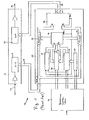
- Fig. 1 illustrates in block diagram form, a prior art line-rotation decoder system 10.
- the system 10 is usable, for example, in connection with a television receiver.
- the system 10 includes an input-output conversion unit 12 which receives scrambled analog composite video signals on a line 14.
- an input-output conversion unit 12 which receives scrambled analog composite video signals on a line 14.
- a line-rotation scrambling operation has previously been performed on each horizonal line signal in the composite video signal received on the line 14.
- the analog composite video signal is first digitized by an analog-to-digital converter (A/D) 16 in the conversion unit 12.
- A/D analog-to-digital converter
- the output of the A/D 16, in the form of 8-bit digital samples, is transmitted via an 8-bit data bus 18 to a decoder unit 20.
- the function of the decoder unit 20 is to reverse the line-rotation scrambling operation performed at the transmission site.
- the unit 20 includes a read-write memory 22.
- the memory 22 includes a plurality of locations for storing 8-bit video data samples received from the bus 18.
- the capacity of the memory 22 is large enough to store a set of digital samples from the bus 18 corresponding to a single horizontal video line.
- the read-write memory 22 may be a random access memory or a serial, shift register, memory.
- the implementation of the memory 22 is conventional in the art.
- Video samples are stored in locations in the memory 22 under the control of a write select address counter 24.
- the write select counter 24 could be, for example, a 10-bit binary counter. Outputs from the write select counter 24 are coupled by a selector circuit 26 to a 10-bit address input of the memory 22.
- the selector circuit 26 could, for example, be a conventional multiplexor. Outputs from the write counter 24 are also coupled to a 10-bit comparator 28.
- a read select address counter 30 is also coupled to the data selector 26 and the comparator 28.
- the memory 32 has the same storage capacity as does the memory 22 and may be implemented in the same manner as the memory 22.
- the counter 30 has been preloaded with-the address of the first sample of the original unscrambled video line by start-address circuitry 34.
- the start address circuitry 34 could be implemented, for example, as a combinational circuit alone or as a combinational circuit combined with a storage register.
- the implementation of the start-address circuitry is conventional in the art.
- a second data selector, or multiplexor, 36 couples the output signals from the memory 32 to a data out bus 38.
- the bus 33 is in turn electrically connected to an 8-bit digital to analog converter (3/A) 40.
- the D/A 40 generates a decoded analog composite video signal on an output line 42 for use by a local television receiver.
- Conventional control logic 44 provides timing and control signals to the system 10.
- the comparator 28 generates an ouput signal or indicia on a line 46 indicating when a predetermined end address has been reached by the read select counter 30.
- the signal on the line 46 can be used to clear the counter 30. Bits or stages of the counter 30 can then be set by the start-address circuitry 34 to a new start-address value for the next line of decoded video information.
- the decoding process is now repeated with the functions of the memories 22 and 32 being interchanged by means of the data selectors 26 and 36.
- the memory 32 will now be loaded with video data samples from the bus 18 for the next line of video under control of the write address counter 24.
- the memory 22 will simultaneously read-out to the selector 36 and the output bus 38, the decoded video samples for the current horizontal line under control of the read address counter 30.
- the system 10 requires memories 22 and 32 for storage of data for the active portion of two video lines, address counters 24 and 30 for each respective memory 22 and 33, and two selectors or multiplexors 26 and 34. For most applications the horizontal blanking interval need not be stored in the memories 22 or 32.
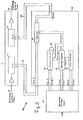
- FIG 2 illustrates a system 50 in accordance with the present invention.
- the system 50 includes the same converter unit 12 and control logic 44 disclosed above and illustrated in Figure 1.
- the system 50 also includes a decoder unit 52 in accordance with the present invention.
- decoder unit 52 uses the identical converter unit 12 as does the prior art decoder unit 20 of Figure 1 and has the same input-output configuration as does the system 10. However, the decoder 52 requires only one-half the storage capacity and fewer control circuits than does the decoder 20.
- the decoder 52 includes a memory 54 with each sample storage location capable of storing 8-bit samples received off of the input bus 18.
- the memory 54 is large enough to store a single, digital, horizontal line of video information.
- Each of the memories 22 and 32 has the same capacity as does the memory 54.
- the memory 54 also may be implemented as a random access memory or a serial, shift register, memory. The exact implementation of the memory 54 is not a limitation of the present invention.
- Address signals are provided to the memory 54 by a 10-bit address counter 56.
- the address counter 56 is also coupled to a 10-bit end address comparator 58.
- Start address circuit 60 provides an initial start address for the address counter 56.
- the address counter 56 could be implemented, for example, as a binary up-counter or alternately as a binary down-counter.
- the address counter 56 is loaded with the start-address of the previous line of video information already stored in the memory 54.
- the previously stored data sample of video information is then read out of the location in the memory 54 addressed by the counter 56.
- the contents of this storage location are overwritten by a new data sample, corresponding to a current line of video information on the bus 18.
- the counter 56 is then pulsed to form a new address. As each prestored sample is output to the bus 38 from an addressed location in the memory 54, that location is immediately overwritten by a new sample of video information from the bus 18. If the counter 56 is an up-counter, it sequentially is incremented to its highest address. The counter 56 then overflows to zero and continues to increment to a value of start-address-minus-1.
- An output signal on a line 62 from the comparator 58 clears the address counter 56 when a predetermined end address value has been reached.
- the input to the comparator 58 can be obtained from the previous end address value sensed for the counter 56 and then used during the next line decoding operation.
- the subsequent lines are rotated in the same manner, without need of the second address counter 30, the second memory 32 or multiplexors.
- the start-address value for a new line in the decoder 52 will be rotated along with the time correcting of the previous line. It is known with respect to the decoder 20 that the relation between the split address at the encryption end and the start-address at the decryption end is given by- the formula: where N is the number of samples per horizontal line of video, ST is the start-address (0 to N-1), and SP is the split address.
- wwqe PST is the start-address used to decrypt the previous line.
- wwqe PST is the start-address used to decrypt the previous line.
- encryption could be hardened further by adding a decriment capability to the address counter 56.
- the line segments could be transmitted in reverse time as well as interchanged.
- the two segments could be independently selected for normal or reverse time,
Landscapes
- Engineering & Computer Science (AREA)
- Multimedia (AREA)
- Signal Processing (AREA)
- Television Systems (AREA)
Applications Claiming Priority (2)
| Application Number | Priority Date | Filing Date | Title |
|---|---|---|---|
| US68265184A | 1984-12-17 | 1984-12-17 | |
| US682651 | 1984-12-17 |
Publications (3)
| Publication Number | Publication Date |
|---|---|
| EP0186056A2 true EP0186056A2 (fr) | 1986-07-02 |
| EP0186056A3 EP0186056A3 (en) | 1987-08-12 |
| EP0186056B1 EP0186056B1 (fr) | 1991-10-16 |
Family
ID=24740592
Family Applications (1)
| Application Number | Title | Priority Date | Filing Date |
|---|---|---|---|
| EP19850115841 Expired EP0186056B1 (fr) | 1984-12-17 | 1985-12-12 | Appareil de décodage vidéo |
Country Status (3)
| Country | Link |
|---|---|
| EP (1) | EP0186056B1 (fr) |
| JP (1) | JPS61216584A (fr) |
| DE (1) | DE3584434D1 (fr) |
Families Citing this family (2)
| Publication number | Priority date | Publication date | Assignee | Title |
|---|---|---|---|---|
| JP2515793B2 (ja) * | 1987-05-02 | 1996-07-10 | 日本放送協会 | 画像デスクランブラ |
| JPH0260291A (ja) * | 1988-08-25 | 1990-02-28 | Matsushita Electric Ind Co Ltd | デスクランブル装置 |
Citations (3)
| Publication number | Priority date | Publication date | Assignee | Title |
|---|---|---|---|---|
| GB1590579A (en) * | 1977-12-16 | 1981-06-03 | Micro Consultants Ltd | Information scrambler system |
| FR2539938A1 (fr) * | 1983-01-25 | 1984-07-27 | Thomson Brandt | Procede de protection du videosignal d'une emission de television notamment a peage et dispositif mettant en oeuvre un tel procede |
| EP0127383A1 (fr) * | 1983-05-27 | 1984-12-05 | M/A-Com Government Systems, Inc. | Systèmes de cryptage et de décryptage de signaux de télévision |
-
1985
- 1985-12-12 DE DE8585115841T patent/DE3584434D1/de not_active Expired - Lifetime
- 1985-12-12 EP EP19850115841 patent/EP0186056B1/fr not_active Expired
- 1985-12-17 JP JP28214585A patent/JPS61216584A/ja active Pending
Patent Citations (3)
| Publication number | Priority date | Publication date | Assignee | Title |
|---|---|---|---|---|
| GB1590579A (en) * | 1977-12-16 | 1981-06-03 | Micro Consultants Ltd | Information scrambler system |
| FR2539938A1 (fr) * | 1983-01-25 | 1984-07-27 | Thomson Brandt | Procede de protection du videosignal d'une emission de television notamment a peage et dispositif mettant en oeuvre un tel procede |
| EP0127383A1 (fr) * | 1983-05-27 | 1984-12-05 | M/A-Com Government Systems, Inc. | Systèmes de cryptage et de décryptage de signaux de télévision |
Also Published As
| Publication number | Publication date |
|---|---|
| DE3584434D1 (de) | 1991-11-21 |
| JPS61216584A (ja) | 1986-09-26 |
| EP0186056B1 (fr) | 1991-10-16 |
| EP0186056A3 (en) | 1987-08-12 |
Similar Documents
| Publication | Publication Date | Title |
|---|---|---|
| KR100343821B1 (ko) | 음성/영상 신호 트랜스포트 프로세서 장치 | |
| KR100357506B1 (ko) | 패킷프로그램성분검출기 | |
| US4292650A (en) | Stv Subscriber address system | |
| US5521979A (en) | Packet video signal inverse transport system | |
| US5802063A (en) | Conditional access filter as for a packet video signal inverse transport system | |
| CA1119303A (fr) | Transmission et/ou enregistrement de signaux numeriques | |
| US4716588A (en) | Addressable subscription television system having multiple scrambling modes | |
| US5613003A (en) | Packet video signal inverse transport processor memory address circuitry | |
| EP0212223B1 (fr) | Codeur de vidéo | |
| EP0679035B1 (fr) | Traitement de codes d'erreur de média, applicable à la décompression de paquets de signaux vidéo numériques | |
| US20080134234A1 (en) | Conditional access filter as for a packet video signal inverse transport system | |
| EP0341801A2 (fr) | Système de brouillage d'images de télévision | |
| EP0186056B1 (fr) | Appareil de décodage vidéo | |
| GB2269507A (en) | Coding a video signal to facilitate aspect ratio conversion | |
| JPS63292788A (ja) | スクランブルされた映像信号の復元装置 | |
| HUT74260A (en) | Method and apparatus for transmitting additional information signals toge ther with videofrequency image signals | |
| KR19990023633U (ko) | 디지탈위성 영상수신기의 스크램블 기능을 구비한 메모리장치 |
Legal Events
| Date | Code | Title | Description |
|---|---|---|---|
| PUAI | Public reference made under article 153(3) epc to a published international application that has entered the european phase |
Free format text: ORIGINAL CODE: 0009012 |
|
| AK | Designated contracting states |
Kind code of ref document: A2 Designated state(s): DE FR GB IT NL |
|
| RAP1 | Party data changed (applicant data changed or rights of an application transferred) |
Owner name: ITT INDUSTRIES INC. |
|
| PUAL | Search report despatched |
Free format text: ORIGINAL CODE: 0009013 |
|
| AK | Designated contracting states |
Kind code of ref document: A3 Designated state(s): DE FR GB IT NL |
|
| 17P | Request for examination filed |
Effective date: 19880128 |
|
| 17Q | First examination report despatched |
Effective date: 19900528 |
|
| GRAA | (expected) grant |
Free format text: ORIGINAL CODE: 0009210 |
|
| AK | Designated contracting states |
Kind code of ref document: B1 Designated state(s): DE FR GB IT NL |
|
| REF | Corresponds to: |
Ref document number: 3584434 Country of ref document: DE Date of ref document: 19911121 |
|
| ET | Fr: translation filed | ||
| ITF | It: translation for a ep patent filed |
Owner name: BUGNION S.P.A. |
|
| PLBE | No opposition filed within time limit |
Free format text: ORIGINAL CODE: 0009261 |
|
| STAA | Information on the status of an ep patent application or granted ep patent |
Free format text: STATUS: NO OPPOSITION FILED WITHIN TIME LIMIT |
|
| 26N | No opposition filed | ||
| PGFP | Annual fee paid to national office [announced via postgrant information from national office to epo] |
Ref country code: GB Payment date: 19941129 Year of fee payment: 10 |
|
| PGFP | Annual fee paid to national office [announced via postgrant information from national office to epo] |
Ref country code: DE Payment date: 19941216 Year of fee payment: 10 |
|
| PGFP | Annual fee paid to national office [announced via postgrant information from national office to epo] |
Ref country code: FR Payment date: 19941230 Year of fee payment: 10 |
|
| PGFP | Annual fee paid to national office [announced via postgrant information from national office to epo] |
Ref country code: NL Payment date: 19941231 Year of fee payment: 10 |
|
| PG25 | Lapsed in a contracting state [announced via postgrant information from national office to epo] |
Ref country code: GB Effective date: 19951212 |
|
| PG25 | Lapsed in a contracting state [announced via postgrant information from national office to epo] |
Ref country code: NL Effective date: 19960701 |
|
| GBPC | Gb: european patent ceased through non-payment of renewal fee |
Effective date: 19951212 |
|
| PG25 | Lapsed in a contracting state [announced via postgrant information from national office to epo] |
Ref country code: FR Effective date: 19960830 |
|
| NLV4 | Nl: lapsed or anulled due to non-payment of the annual fee |
Effective date: 19960701 |
|
| PG25 | Lapsed in a contracting state [announced via postgrant information from national office to epo] |
Ref country code: DE Effective date: 19960903 |
|
| REG | Reference to a national code |
Ref country code: FR Ref legal event code: ST |