EP0183517A2 - Semiconductor memory device wirings - Google Patents
Semiconductor memory device wirings Download PDFInfo
- Publication number
- EP0183517A2 EP0183517A2 EP85308564A EP85308564A EP0183517A2 EP 0183517 A2 EP0183517 A2 EP 0183517A2 EP 85308564 A EP85308564 A EP 85308564A EP 85308564 A EP85308564 A EP 85308564A EP 0183517 A2 EP0183517 A2 EP 0183517A2
- Authority
- EP
- European Patent Office
- Prior art keywords
- wirings
- wiring
- wiring groups
- memory cell
- cell structures
- Prior art date
- Legal status (The legal status is an assumption and is not a legal conclusion. Google has not performed a legal analysis and makes no representation as to the accuracy of the status listed.)
- Granted
Links
Images


Classifications
-
- H—ELECTRICITY
- H01—ELECTRIC ELEMENTS
- H01L—SEMICONDUCTOR DEVICES NOT COVERED BY CLASS H10
- H01L23/00—Details of semiconductor or other solid state devices
- H01L23/48—Arrangements for conducting electric current to or from the solid state body in operation, e.g. leads, terminal arrangements ; Selection of materials therefor
-
- H—ELECTRICITY
- H01—ELECTRIC ELEMENTS
- H01L—SEMICONDUCTOR DEVICES NOT COVERED BY CLASS H10
- H01L23/00—Details of semiconductor or other solid state devices
- H01L23/52—Arrangements for conducting electric current within the device in operation from one component to another, i.e. interconnections, e.g. wires, lead frames
- H01L23/522—Arrangements for conducting electric current within the device in operation from one component to another, i.e. interconnections, e.g. wires, lead frames including external interconnections consisting of a multilayer structure of conductive and insulating layers inseparably formed on the semiconductor body
- H01L23/5222—Capacitive arrangements or effects of, or between wiring layers
-
- H—ELECTRICITY
- H01—ELECTRIC ELEMENTS
- H01L—SEMICONDUCTOR DEVICES NOT COVERED BY CLASS H10
- H01L23/00—Details of semiconductor or other solid state devices
- H01L23/52—Arrangements for conducting electric current within the device in operation from one component to another, i.e. interconnections, e.g. wires, lead frames
- H01L23/522—Arrangements for conducting electric current within the device in operation from one component to another, i.e. interconnections, e.g. wires, lead frames including external interconnections consisting of a multilayer structure of conductive and insulating layers inseparably formed on the semiconductor body
- H01L23/528—Geometry or layout of the interconnection structure
- H01L23/5283—Cross-sectional geometry
-
- H—ELECTRICITY
- H01—ELECTRIC ELEMENTS
- H01L—SEMICONDUCTOR DEVICES NOT COVERED BY CLASS H10
- H01L27/00—Devices consisting of a plurality of semiconductor or other solid-state components formed in or on a common substrate
- H01L27/02—Devices consisting of a plurality of semiconductor or other solid-state components formed in or on a common substrate including semiconductor components specially adapted for rectifying, oscillating, amplifying or switching and having at least one potential-jump barrier or surface barrier; including integrated passive circuit elements with at least one potential-jump barrier or surface barrier
- H01L27/04—Devices consisting of a plurality of semiconductor or other solid-state components formed in or on a common substrate including semiconductor components specially adapted for rectifying, oscillating, amplifying or switching and having at least one potential-jump barrier or surface barrier; including integrated passive circuit elements with at least one potential-jump barrier or surface barrier the substrate being a semiconductor body
- H01L27/10—Devices consisting of a plurality of semiconductor or other solid-state components formed in or on a common substrate including semiconductor components specially adapted for rectifying, oscillating, amplifying or switching and having at least one potential-jump barrier or surface barrier; including integrated passive circuit elements with at least one potential-jump barrier or surface barrier the substrate being a semiconductor body including a plurality of individual components in a repetitive configuration
-
- H—ELECTRICITY
- H01—ELECTRIC ELEMENTS
- H01L—SEMICONDUCTOR DEVICES NOT COVERED BY CLASS H10
- H01L2924/00—Indexing scheme for arrangements or methods for connecting or disconnecting semiconductor or solid-state bodies as covered by H01L24/00
- H01L2924/0001—Technical content checked by a classifier
- H01L2924/0002—Not covered by any one of groups H01L24/00, H01L24/00 and H01L2224/00
Definitions
- the present invention relates to semiconductor memory device wirings (wiring lines).
- the semiconductor device may be a dynamic random-access memory (RAM), a static RAM, or a read-only memory (ROM).
- RAM dynamic random-access memory
- ROM read-only memory
- DRAM dynamic RAM
- the pitch of the plurality of data lines must be reduced to achieve a high-density DRAM having fine memory cells with a high packing density. As a result, the width of each of the data lines must be decreased.
- the wiring pitch is 3.5 ⁇ m.
- the wiring width of a contact pad is/larger than the wiring width by, for example, 0.5 ⁇ m
- the wiring width is made to be 1.5 ⁇ m and the wiring interval is accordingly 1.5 ⁇ m.
- the wiring width and the wiring interval must be decreased to about 0.8 ⁇ m to 0.5 ⁇ m under the condition wherein the same margin (i.e., 0.5 ⁇ m larger than the wiring width) as described above is given to the contact pad.
- the wiring width is greatly decreased, the cross-sections of the wirings are greatly decreased, the wiring resistance is increased, and hence the electromigration effect is increased. Accordingly, the operation speed and the reliability of the semiconductor memory device are deteriorated.
- the cross-sections of the wirings may no longer be ensured to be of sufficient size.
- a semiconductor memory device comprising:
- An embodiment of the present invention may provide a new and improved semiconductor memory device wherein a width of each wiring can be ensured, a cross-section thereof is maintained to be larger than a predetermined value, and the operation speed and the reliability of the device are not deteriorated even if the device is highly integrated.
- a semiconductor memory device including: a semiconductor substrate; a plurality of memory cell structures formed on the semiconductor substrate; a plurality of wiring groups formed above the memory cell structures for providing data lines for predetermined functions, wirings of the wiring group extending in parallel along a predetermined direction; and insulating interlayers between wirings of the wiring groups.
- Wirings of one of the wiring groups for a predetermined function may be distributed between an upper layer and a lower layer separated by one of the insulating interlayers, and wirings distributed in the upper layer may be arranged in an overlapped relationship with regard to wirings distributed in the lower layer.
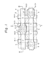
- Figures 2 and 3 are sectional views of the DRAM of Fig. 1 taken along the lines II-II and III-III.
- Figure 4 shows the circuit structure of the device of Fig. 1.
- Reference numeral 1 denotes a p type silicon substrate; 2 an element isolation oxide film; 3 a silicon dioxide (Si0 2 ) dielectric film; 4 a capacitor electrode of a first polycrystalline silicon layer; 5 an n + type region as one electrode of the capacitor; 6 a gate oxide film; 7 an Si0 2 insulating film; 8(1), 8(2), 8(3), and 8(4) address lines (gate electrodes) of a second polycrystalline silicon layer, respectively; 9 an n + type drain region; 10 a phosphosilicate glass (PSG) insulating interlayer; 11 a contact hole; 12 a contact pad; and 19(1), 19(2), 19(3), and 19(4) data lines of a single aluminum film.
- the transistor regions T, the capacitance region C, the word lines, and a bit line.in Fig. 1 are shown correspondingly in the circuit structure of Fig. 4.
- the parallel data lines 19(1) to 19(4) are constituted by a single aluminum film.
- the interval of the data lines 19(1) to 19(4) must be / decreased, and the width of each of the data lines 19(1) to 19(4) must be decreased, upon further micropatterning of the memory cells.
- the wiring width and the wiring interval are given as 1.5 um. This width has been used in -recent 256 Kbit or 1 Mbit DRAM's. When the DRAM is highly integrated and the wiring pitch is decreased to about 2.0 to 1.5 um, the wiring width and the wiring interval must be decreased to 0.75 to 0.5 ⁇ m when the margin of the contact pad is given as described above.
- a semiconductor memory device according to an embodiment of the present invention is illustrated in Figs. 5 to 8.
- Figure 5 is a plan view of a DRAM
- Fig. 6 is a sectional view thereof taken along the line VI-VI of Fig. 5.
- a wiring portion of the DRAM of Fig. 1 and that of the DRAM of Fig. 5 are illustrated in Figs. 8A and 8B.
- Figure 8 shows the circuit structure of the device of Fig. 5.
- Figure 9 shows a modification of the wiring pattern.
- reference numeral 1 denotes a p type silicon substrate; 2 an element isolation oxide film; 3 an Si0 2 dielectric film; 4 a capacitor electrode of a first polycrystalline silicon layer PA; 5 an-n + type region serving as one electrode of the capacitor; 6 a gate oxide film; 7 an Si0 2 insulating film; 8(1), 8(2), 8(3), and 8(4) gate electrodes serving as address lines made of a second polycrystalline silicon layer PB, respectively; 9 an n + type drain region; 10 a first PSG insulating interlayer; 13 a contact, hole between a lower wiring layer and the drain region 9; 14 a second PSG insulating interlayer; and 15 a contact hole between the upper wiring layer and the drain region 9.
- Reference numerals 17(2) and 17(1) are lower data lines made of a lower aluminum film, respectively; 18(2) and 18(1) are upper data lines made of an upper aluminum film.
- Each memory cell includes one transistor T and one capacitor C as in the previous device.
- a plurality of parallel data lines,sequentially constituted by a wiring layer of a single wiring material such as aluminum, are alternately formed by the upper and lower aluminum films rom each other insulated/through the second insulating interlayer 14 in an order of 17(2), 18(2), 17(1), and 18(1). Further, in this example /the data lines 18(2) and 18(1) formed by the upper aluminum film overlap the adjacent data lines of the lower aluminum film, respectively.
- a previous structure has data lines of a single layer. Assume that parallel data lines 19(1), 19(2), ... 19(7) are formed in a wiring region at a wiring width of ld and a wiring interval of ld. However, as shown in Fig. 9B, the data lines 18(1), 17(2), 18(2), 17(3), 18(3), 17(4), and 18(4) can be formed in the same wiring area as that of the previous
- the wiring width of the data linesof the DRAM of this embodiment can be increased to three times that of the previous DRAM.
- recesses 16 may be formed in the lower data lines 17(2) and 17(3) to (avoid) detour/the contact holesl5 formed between the upper data lines 18(2) and 18(3).
- the width of the lower data lines 17(2) and 17(3) can be larger than that shown in Fig. 5 up to that defined by a maximum interval defined by insulation and connection of the wirings of (single) an identical/layer.
- the upper data lines 18(2) and 18(3) do not have the limits described above, so the wiring width can be maximized in association with a minimum wiring interval.
- FIG. 11 A preferred circuit diagram applicable to an embodiment of the present invention in connection with sense amplifiers is shown in Fig. 11.
- the circuit arrangement shown in Fig. 11 requires a slight modification of the layout structure of Fig. 5, but has an advantage of a superior symmetrization of electrical characteristicsbetween data line pairs associated with a sense amplifier, which is desirable in DRAMs.
- Data lines DL 0 and DL 0 connected with the first sense amplifier are located in the upper layer.
- Data lines DL1 and DL 1 connected with the second sense amplifier are and so forth. located in the lower layer,/
- the present invention is exemplified by a DRAM. However, the present invention can also be applied to other semiconductor memory devices such as static RAM's and static ROM's.
- the wiring material is not limited to aluminum, but may comprise any other suitable material.
Abstract
Description
- The present invention relates to semiconductor memory device wirings (wiring lines).
- The semiconductor device may be a dynamic random-access memory (RAM), a static RAM, or a read-only memory (ROM).
- In a previous dynamic RAM (DRAM), a plurality of parallel data lines are constituted by a single aluminum film.
- With a structure wherein a plurality of data lines are formed by a wiring material such as a single aluminum film, the pitch of the plurality of data lines must be reduced to achieve a high-density DRAM having fine memory cells with a high packing density. As a result, the width of each of the data lines must be decreased.
- Assume that the wiring pitch is 3.5 µm. In required to be this case, when the width of a contact pad is/larger than the wiring width by, for example, 0.5 µm, the wiring width is made to be 1.5 µm and the wiring interval is accordingly 1.5 µm. These values may be applicable for a 256-Kbit or 1-Mbit DRAM.
- When the packing density of the DRAM is in the range increased and the wiring pitch is decreased to/2.1 µm to 1.5 µm, the wiring width and the wiring interval must be decreased to about 0.8 µm to 0.5 µm under the condition wherein the same margin (i.e., 0.5 µm larger than the wiring width) as described above is given to the contact pad.
- In a very large-scale semiconductor memory device of a DRAM of which a structure of high concentration and high integration is required, with such a wiring structure, the wiring width is greatly decreased, the cross-sections of the wirings are greatly decreased, the wiring resistance is increased, and hence the electromigration effect is increased. Accordingly, the operation speed and the reliability of the semiconductor memory device are deteriorated. The cross-sections of the wirings may no longer be ensured to be of sufficient size.
- According to the present invention there is provided a semiconductor memory device comprising:
- a semiconductor substrate;
- a plurality of memory cell structures formed on said semiconductor substrate;
- a plurality of wiring groups with insulating interlayers therebetween, for said memory cell structures for providing data lines for predetermined functions, wirings in each of said wiring groups extending in parallel within the group, and wirings within one of said wiring groups being distributed between an upper layer and a lower layer separated by an insulating interlayer.
- An embodiment of the present invention may provide a new and improved semiconductor memory device wherein a width of each wiring can be ensured, a cross-section thereof is maintained to be larger than a predetermined value, and the operation speed and the reliability of the device are not deteriorated even if the device is highly integrated.
- There may be provided a semiconductor memory device including: a semiconductor substrate; a plurality of memory cell structures formed on the semiconductor substrate; a plurality of wiring groups formed above the memory cell structures for providing data lines for predetermined functions, wirings of the wiring group extending in parallel along a predetermined direction; and insulating interlayers between wirings of the wiring groups. Wirings of one of the wiring groups for a predetermined function may be distributed between an upper layer and a lower layer separated by one of the insulating interlayers, and wirings distributed in the upper layer may be arranged in an overlapped relationship with regard to wirings distributed in the lower layer.
- Reference is made, by way of example, to the accompanying drawings in which:
- Fig. 1 is a plan view showing a main part of a previous semiconductor memory device;
- Fig. 2 is a sectional view thereof taken along the line II-II of Fig. 1;
- Fig. 3 is a sectional view thereof taken along the line III-III of Fig. 1;
- Fig. 4 shows the circuit structure of the device of Fig. 1;
- Fig. 5 is a plan view showing a main part of a DRAM according to an embodiment of the present invention;
- Fig. 6 is a sectional view thereof taken along the line VI-VI of Fig. 5;
- Fig. 7 is a sectional view thereof taken along the line VII-VII of Fig. 5;
- Fig. 8 shows a circuit structure of the device of Fig. 5;
- Figs. 9A and 9B are sectional views of a of the device of Fig. 1 wiring portion/and a wiring portion of the DRAM of Fig. 5;
- Fig. 10 is a plan view showing a modification of the wiring pattern; and
- Fig. 11 shows a circuit diagram applicable to an embodiment of the present invention.
- Before entering into a description of the embodiment, a previous DRAM will be described with reference to Figs. 1 to 4. Figures 2 and 3 are sectional views of the DRAM of Fig. 1 taken along the lines II-II and III-III. Figure 4 shows the circuit structure of the device of Fig. 1.
Reference numeral 1 denotes a p type silicon substrate; 2 an element isolation oxide film; 3 a silicon dioxide (Si02) dielectric film; 4 a capacitor electrode of a first polycrystalline silicon layer; 5 an n+ type region as one electrode of the capacitor; 6 a gate oxide film; 7 an Si02 insulating film; 8(1), 8(2), 8(3), and 8(4) address lines (gate electrodes) of a second polycrystalline silicon layer, respectively; 9 an n+ type drain region; 10 a phosphosilicate glass (PSG) insulating interlayer; 11 a contact hole; 12 a contact pad; and 19(1), 19(2), 19(3), and 19(4) data lines of a single aluminum film. The transistor regions T, the capacitance region C, the word lines, and a bit line.in Fig. 1 are shown correspondingly in the circuit structure of Fig. 4. - In the previous DRAM shown in Figs. 1 to 4, the parallel data lines 19(1) to 19(4) are constituted by a single aluminum film.
- However, in a structure wherein the data lines 19(1) to 19(4) are constituted by a single wiring material layer, e.g., the aluminum film in this example, the interval of the data lines 19(1) to 19(4) must be / decreased, and the width of each of the data lines 19(1) to 19(4) must be decreased, upon further micropatterning of the memory cells.
- In the structure shown in Figs. 1 to 4, when the wiring pitch is given as 3.5 µm and a width of the
contact pad 12 is required to be larger by, for example, 0.5 µm than the wiring width, the wiring width and the wiring interval are given as 1.5 um. This width has been used in -recent 256 Kbit or 1 Mbit DRAM's. When the DRAM is highly integrated and the wiring pitch is decreased to about 2.0 to 1.5 um, the wiring width and the wiring interval must be decreased to 0.75 to 0.5 µm when the margin of the contact pad is given as described above. - A semiconductor memory device according to an embodiment of the present invention is illustrated in Figs. 5 to 8.
- Figure 5 is a plan view of a DRAM, and Fig. 6 is a sectional view thereof taken along the line VI-VI of Fig. 5. A wiring portion of the DRAM of Fig. 1 and that of the DRAM of Fig. 5 are illustrated in Figs. 8A and 8B. Figure 8 shows the circuit structure of the device of Fig. 5. Figure 9 shows a modification of the wiring pattern.
- Referring to Figs. 5 to 8,
reference numeral 1 denotes a p type silicon substrate; 2 an element isolation oxide film; 3 an Si02 dielectric film; 4 a capacitor electrode of a first polycrystalline silicon layer PA; 5 an-n+ type region serving as one electrode of the capacitor; 6 a gate oxide film; 7 an Si02 insulating film; 8(1), 8(2), 8(3), and 8(4) gate electrodes serving as address lines made of a second polycrystalline silicon layer PB, respectively; 9 an n+ type drain region; 10 a first PSG insulating interlayer; 13 a contact, hole between a lower wiring layer and thedrain region 9; 14 a second PSG insulating interlayer; and 15 a contact hole between the upper wiring layer and thedrain region 9. Reference numerals 17(2) and 17(1) are lower data lines made of a lower aluminum film, respectively; 18(2) and 18(1) are upper data lines made of an upper aluminum film. Each memory cell includes one transistor T and one capacitor C as in the previous device. - In the DRAM shown in Fig. 5, a plurality of parallel data lines,sequentially constituted by a wiring layer of a single wiring material such as aluminum, are alternately formed by the upper and lower aluminum films rom each other insulated/through the second
insulating interlayer 14 in an order of 17(2), 18(2), 17(1), and 18(1). Further, in this example /the data lines 18(2) and 18(1) formed by the upper aluminum film overlap the adjacent data lines of the lower aluminum film, respectively. - As shown in Fig. 9A, a previous structure has data lines of a single layer. Assume that parallel data lines 19(1), 19(2), ... 19(7) are formed in a wiring region at a wiring width of ld and a wiring interval of ld. However, as shown in Fig. 9B, the data lines 18(1), 17(2), 18(2), 17(3), 18(3), 17(4), and 18(4) can be formed in the same wiring area as that of the previous
- DRAM at a wiring width of 3d and a wiring interval of ld. Therefore, the wiring width of the data linesof the DRAM of this embodiment can be increased to three times that of the previous DRAM.
- As shown in Fig. 10, for example,
recesses 16 may be formed in the lower data lines 17(2) and 17(3) to (avoid) detour/the contact holesl5 formed between the upper data lines 18(2) and 18(3). In this case, the width of the lower data lines 17(2) and 17(3) can be larger than that shown in Fig. 5 up to that defined by a maximum interval defined by insulation and connection of the wirings of (single) an identical/layer. - However, the upper data lines 18(2) and 18(3) do not have the limits described above, so the wiring width can be maximized in association with a minimum wiring interval.
- A preferred circuit diagram applicable to an embodiment of the present invention in connection with sense amplifiers is shown in Fig. 11.
- The circuit arrangement shown in Fig. 11 requires a slight modification of the layout structure of Fig. 5, but has an advantage of a superior symmetrization of electrical characteristicsbetween data line pairs associated with a sense amplifier, which is desirable in DRAMs. Data lines DL0 and
DL 0 connected with the first sense amplifier are located in the upper layer. Data lines DL1 andDL 1 connected with the second sense amplifier are and so forth. located in the lower layer,/ In the circuit arrangement of Fig. 11, where the data lines are divided into a first group of data lines DL and a second group of data lines DL, the characteristic of symmetry between the ( for example, bit lines and dummy it ines data lines/is attained satisfactorily. - The present invention is exemplified by a DRAM. However, the present invention can also be applied to other semiconductor memory devices such as static RAM's and static ROM's.
- The wiring material is not limited to aluminum, but may comprise any other suitable material.
Claims (7)
Applications Claiming Priority (2)
| Application Number | Priority Date | Filing Date | Title |
|---|---|---|---|
| JP248946/84 | 1984-11-26 | ||
| JP59248946A JPS61127161A (en) | 1984-11-26 | 1984-11-26 | Semiconductor memory |
Publications (3)
| Publication Number | Publication Date |
|---|---|
| EP0183517A2 true EP0183517A2 (en) | 1986-06-04 |
| EP0183517A3 EP0183517A3 (en) | 1986-12-30 |
| EP0183517B1 EP0183517B1 (en) | 1989-03-22 |
Family
ID=17185768
Family Applications (1)
| Application Number | Title | Priority Date | Filing Date |
|---|---|---|---|
| EP85308564A Expired EP0183517B1 (en) | 1984-11-26 | 1985-11-26 | Semiconductor memory device wirings |
Country Status (5)
| Country | Link |
|---|---|
| US (1) | US4807017A (en) |
| EP (1) | EP0183517B1 (en) |
| JP (1) | JPS61127161A (en) |
| KR (1) | KR900000634B1 (en) |
| DE (1) | DE3569067D1 (en) |
Cited By (4)
| Publication number | Priority date | Publication date | Assignee | Title |
|---|---|---|---|---|
| DE3807162A1 (en) * | 1987-07-02 | 1989-01-12 | Mitsubishi Electric Corp | SEMICONDUCTOR MEMORY DEVICE |
| FR2638285A1 (en) * | 1988-10-25 | 1990-04-27 | Commissariat Energie Atomique | HIGH-DENSITY INTEGRATED INTEGRATED CIRCUIT SUCH AS MEMORY EPROM AND CORRESPONDING OBTAINING METHOD |
| US4984199A (en) * | 1986-09-09 | 1991-01-08 | Mitsubishi Denki Kabushiki Kaisha | Semiconductor memory cells having common contact hole |
| WO1998024127A1 (en) * | 1996-11-26 | 1998-06-04 | Philips Electronics N.V. | Electrically erasable and programmable read only memory (eeprom) having multiple overlapping metallization layers |
Families Citing this family (9)
| Publication number | Priority date | Publication date | Assignee | Title |
|---|---|---|---|---|
| JPH07120755B2 (en) * | 1986-10-24 | 1995-12-20 | 日本電気株式会社 | Semiconductor memory device |
| JP2712079B2 (en) * | 1988-02-15 | 1998-02-10 | 株式会社東芝 | Semiconductor device |
| JPH0263163A (en) * | 1988-08-29 | 1990-03-02 | Nec Corp | Nonvolatile semiconductor storage device |
| JP2503661B2 (en) * | 1989-06-28 | 1996-06-05 | 日本電気株式会社 | Semiconductor memory device and manufacturing method thereof |
| JPH03109767A (en) * | 1989-09-25 | 1991-05-09 | Nec Corp | Semiconductor integrated circuit device |
| US5170243A (en) * | 1991-11-04 | 1992-12-08 | International Business Machines Corporation | Bit line configuration for semiconductor memory |
| JPH09252058A (en) * | 1996-03-15 | 1997-09-22 | Rohm Co Ltd | Semiconductor memory device and manufacture thereof |
| US5877976A (en) * | 1997-10-28 | 1999-03-02 | International Business Machines Corporation | Memory system having a vertical bitline topology and method therefor |
| DE10155023B4 (en) * | 2001-11-05 | 2008-11-06 | Qimonda Ag | Line arrangement for bit lines for contacting at least one memory cell and method for producing a line arrangement for bit lines |
Citations (6)
| Publication number | Priority date | Publication date | Assignee | Title |
|---|---|---|---|---|
| US3946421A (en) * | 1974-06-28 | 1976-03-23 | Texas Instruments Incorporated | Multi phase double level metal charge coupled device |
| US4001871A (en) * | 1968-06-17 | 1977-01-04 | Nippon Electric Company, Ltd. | Semiconductor device |
| FR2390009A1 (en) * | 1977-05-06 | 1978-12-01 | Siemens Ag | |
| US4206471A (en) * | 1977-09-28 | 1980-06-03 | Siemens Aktiengesellschaft | Semiconductor storage element and a process for the production thereof |
| EP0033130A2 (en) * | 1980-01-25 | 1981-08-05 | Kabushiki Kaisha Toshiba | Semiconductor memory device |
| EP0112670A1 (en) * | 1982-12-20 | 1984-07-04 | Fujitsu Limited | Semiconductor memory device having stacked capacitor-tape memory cells |
Family Cites Families (2)
| Publication number | Priority date | Publication date | Assignee | Title |
|---|---|---|---|---|
| US4328563A (en) * | 1979-01-12 | 1982-05-04 | Mostek Corporation | High density read only memory |
| US4536941A (en) * | 1980-03-21 | 1985-08-27 | Kuo Chang Kiang | Method of making high density dynamic memory cell |
-
1984
- 1984-11-26 JP JP59248946A patent/JPS61127161A/en active Pending
-
1985
- 1985-11-26 EP EP85308564A patent/EP0183517B1/en not_active Expired
- 1985-11-26 KR KR1019850008822A patent/KR900000634B1/en not_active IP Right Cessation
- 1985-11-26 DE DE8585308564T patent/DE3569067D1/en not_active Expired
-
1988
- 1988-06-06 US US07/203,634 patent/US4807017A/en not_active Expired - Fee Related
Patent Citations (6)
| Publication number | Priority date | Publication date | Assignee | Title |
|---|---|---|---|---|
| US4001871A (en) * | 1968-06-17 | 1977-01-04 | Nippon Electric Company, Ltd. | Semiconductor device |
| US3946421A (en) * | 1974-06-28 | 1976-03-23 | Texas Instruments Incorporated | Multi phase double level metal charge coupled device |
| FR2390009A1 (en) * | 1977-05-06 | 1978-12-01 | Siemens Ag | |
| US4206471A (en) * | 1977-09-28 | 1980-06-03 | Siemens Aktiengesellschaft | Semiconductor storage element and a process for the production thereof |
| EP0033130A2 (en) * | 1980-01-25 | 1981-08-05 | Kabushiki Kaisha Toshiba | Semiconductor memory device |
| EP0112670A1 (en) * | 1982-12-20 | 1984-07-04 | Fujitsu Limited | Semiconductor memory device having stacked capacitor-tape memory cells |
Cited By (6)
| Publication number | Priority date | Publication date | Assignee | Title |
|---|---|---|---|---|
| US4984199A (en) * | 1986-09-09 | 1991-01-08 | Mitsubishi Denki Kabushiki Kaisha | Semiconductor memory cells having common contact hole |
| DE3807162A1 (en) * | 1987-07-02 | 1989-01-12 | Mitsubishi Electric Corp | SEMICONDUCTOR MEMORY DEVICE |
| US4887137A (en) * | 1987-07-02 | 1989-12-12 | Mitsubishi Denki Kabushiki Kaisha | Semiconductor memory device |
| FR2638285A1 (en) * | 1988-10-25 | 1990-04-27 | Commissariat Energie Atomique | HIGH-DENSITY INTEGRATED INTEGRATED CIRCUIT SUCH AS MEMORY EPROM AND CORRESPONDING OBTAINING METHOD |
| EP0369842A1 (en) * | 1988-10-25 | 1990-05-23 | Commissariat A L'energie Atomique | Method for the production of a large-scale integrated circuit such as an EPROM |
| WO1998024127A1 (en) * | 1996-11-26 | 1998-06-04 | Philips Electronics N.V. | Electrically erasable and programmable read only memory (eeprom) having multiple overlapping metallization layers |
Also Published As
| Publication number | Publication date |
|---|---|
| JPS61127161A (en) | 1986-06-14 |
| EP0183517B1 (en) | 1989-03-22 |
| KR900000634B1 (en) | 1990-02-01 |
| EP0183517A3 (en) | 1986-12-30 |
| US4807017A (en) | 1989-02-21 |
| KR860004461A (en) | 1986-06-23 |
| DE3569067D1 (en) | 1989-04-27 |
Similar Documents
| Publication | Publication Date | Title |
|---|---|---|
| US4651183A (en) | High density one device memory cell arrays | |
| US5032882A (en) | Semiconductor device having trench type structure | |
| US4638458A (en) | Semiconductor memory address lines with varied interval contact holes | |
| KR840007312A (en) | Semiconductor Memory with Multilayer Capacitor Memory Cells | |
| EP0183517B1 (en) | Semiconductor memory device wirings | |
| KR970060452A (en) | Semiconductor integrated circuit device and manufacturing method thereof | |
| US4809046A (en) | Semiconductor memory device | |
| US5177574A (en) | Semiconductor memory device having a stacked type capacitor and manufacturing method therefor | |
| KR860000716A (en) | Dynamic memory cell and manufacturing method | |
| JP2511415B2 (en) | Semiconductor device | |
| US4631705A (en) | Semiconductor integrated circuit memory device | |
| US4131906A (en) | Dynamic random access memory using MOS FETs and method for manufacturing same | |
| JPH0817942A (en) | Semiconductor storage device | |
| JPH0745722A (en) | Semiconductor storage device | |
| US5770874A (en) | High density semiconductor memory device | |
| KR20020071182A (en) | Semiconductor memory device and method for manufactuirng the same | |
| US4173819A (en) | Method of manufacturing a dynamic random access memory using MOS FETS | |
| US5219781A (en) | Method for manufacturing semiconductor memory device having a stacked type capacitor | |
| KR19990067503A (en) | Semiconductor Interlayer Staggered Contact Structure | |
| JPS6123361A (en) | Semiconductor memory device | |
| JP3147144B2 (en) | Semiconductor device and manufacturing method thereof | |
| US5049958A (en) | Stacked capacitors for VLSI semiconductor devices | |
| JPH07202022A (en) | Semiconductor storage device | |
| JP2604128B2 (en) | Semiconductor device | |
| JPH09167796A (en) | Ferroelectric storage device |
Legal Events
| Date | Code | Title | Description |
|---|---|---|---|
| PUAI | Public reference made under article 153(3) epc to a published international application that has entered the european phase |
Free format text: ORIGINAL CODE: 0009012 |
|
| AK | Designated contracting states |
Kind code of ref document: A2 Designated state(s): DE FR GB |
|
| PUAL | Search report despatched |
Free format text: ORIGINAL CODE: 0009013 |
|
| AK | Designated contracting states |
Kind code of ref document: A3 Designated state(s): DE FR GB |
|
| 17P | Request for examination filed |
Effective date: 19870202 |
|
| 17Q | First examination report despatched |
Effective date: 19880803 |
|
| GRAA | (expected) grant |
Free format text: ORIGINAL CODE: 0009210 |
|
| AK | Designated contracting states |
Kind code of ref document: B1 Designated state(s): DE FR GB |
|
| REF | Corresponds to: |
Ref document number: 3569067 Country of ref document: DE Date of ref document: 19890427 |
|
| ET | Fr: translation filed | ||
| PLBE | No opposition filed within time limit |
Free format text: ORIGINAL CODE: 0009261 |
|
| STAA | Information on the status of an ep patent application or granted ep patent |
Free format text: STATUS: NO OPPOSITION FILED WITHIN TIME LIMIT |
|
| 26N | No opposition filed | ||
| PGFP | Annual fee paid to national office [announced via postgrant information from national office to epo] |
Ref country code: GB Payment date: 19920903 Year of fee payment: 8 |
|
| PGFP | Annual fee paid to national office [announced via postgrant information from national office to epo] |
Ref country code: FR Payment date: 19921127 Year of fee payment: 8 |
|
| PGFP | Annual fee paid to national office [announced via postgrant information from national office to epo] |
Ref country code: DE Payment date: 19930129 Year of fee payment: 8 |
|
| PG25 | Lapsed in a contracting state [announced via postgrant information from national office to epo] |
Ref country code: GB Effective date: 19931126 |
|
| GBPC | Gb: european patent ceased through non-payment of renewal fee |
Effective date: 19931126 |
|
| PG25 | Lapsed in a contracting state [announced via postgrant information from national office to epo] |
Ref country code: FR Effective date: 19940729 |
|
| PG25 | Lapsed in a contracting state [announced via postgrant information from national office to epo] |
Ref country code: DE Effective date: 19940802 |
|
| REG | Reference to a national code |
Ref country code: FR Ref legal event code: ST |