EP0180239B1 - Content-addressable memory - Google Patents
Content-addressable memory Download PDFInfo
- Publication number
- EP0180239B1 EP0180239B1 EP85113907A EP85113907A EP0180239B1 EP 0180239 B1 EP0180239 B1 EP 0180239B1 EP 85113907 A EP85113907 A EP 85113907A EP 85113907 A EP85113907 A EP 85113907A EP 0180239 B1 EP0180239 B1 EP 0180239B1
- Authority
- EP
- European Patent Office
- Prior art keywords
- column
- memory
- signal
- search
- columns
- Prior art date
- Legal status (The legal status is an assumption and is not a legal conclusion. Google has not performed a legal analysis and makes no representation as to the accuracy of the status listed.)
- Expired - Lifetime
Links
Images


Classifications
-
- G—PHYSICS
- G11—INFORMATION STORAGE
- G11C—STATIC STORES
- G11C15/00—Digital stores in which information comprising one or more characteristic parts is written into the store and in which information is read-out by searching for one or more of these characteristic parts, i.e. associative or content-addressed stores
- G11C15/04—Digital stores in which information comprising one or more characteristic parts is written into the store and in which information is read-out by searching for one or more of these characteristic parts, i.e. associative or content-addressed stores using semiconductor elements
-
- G—PHYSICS
- G06—COMPUTING OR CALCULATING; COUNTING
- G06F—ELECTRIC DIGITAL DATA PROCESSING
- G06F16/00—Information retrieval; Database structures therefor; File system structures therefor
- G06F16/90—Details of database functions independent of the retrieved data types
- G06F16/903—Querying
- G06F16/90335—Query processing
- G06F16/90339—Query processing by using parallel associative memories or content-addressable memories
Definitions
- the present invention relates to a content-addressable memory or a memory device which is capable of addressing according to memory contents.
- CAMs content-addressable memories
- a CAM is used to memorize the correspondence between sectors of a buffer memory and addresses of a main memory, so that a address mapping from logical address to physical address can be carried out at a high speed by means of memory content search.
- This type of CAM needs content-addressable memory cells each of which is provided with a circuit for detecting equivalence or coincidence between the memory content and the search information for each memory cell. Accordingly, the memory cells for this CAM are more complicated than those used in a conventional memory device accessed on the basis of the address of a location which stores a desired data.
- the cost per bit amounts to several ten times as much as that of the conventional memory.
- an improved CAM has been developed in which conventional memory cells are used for the store of information and one equivalence detecting circuit is provided for every word unit.
- this type of CAM still is disadvantageous in that search operations have to be executed the times corresponding to the bit number of each word.
- another CAM composed of two conventional memories: the first memory stores data by using search information as an address input, while the second memory receives data or the read-out output from the first memory as an address input and stores search information.
- This type of CAM is disclosed in Japanese Patent Laid-Open No. 73039/74. It is advantageous that the CAM is constructed only with conventional memory cells.
- the CAM has, however, such an disadvantage that the number of necessary memory cells is rapidly increased with increase in the bit number of search information or data, resulting in extreme elevation of cost.
- US-A-3 644 904 discloses a hybrid associative memory comprising a selected number of chips that each have an array of non-associatively addressable binary storage circuits which is arranged in a row and column matrix, wherein each column represents a bit position of words selected in the memory and the rows provide additional word capacity.
- the memory further include a search register storing a word that is to be searched identically for in the memory. Thus this memory is only capable of searching memory information identical with the search information but not memory information having Hamming distance.
- a CAM having a character of ambiguity is desired for applications to fields of pattern recognition or natural language processing.
- such a CAM is desirable to be capable of searching data within a given Hamming distance.
- such a search was performed by introducing an error correcting code. Therefore, the construction of the CAM became complicated, which resulted in the increase of cost.
- CAM content-addressable memory
- said content-addressable memory device comprising: memory means including a matrix of conventional memory cells of k x 2 M rows by m x N pairs of columns, wherein each dataword is stored in said m pairs of columns corresponding to its associated address j and whereby in every first column of a said pair the dataword itself is stored, while in the other column a dataword having a certain functional relation to said dataword is stored; row selecting means coupled to said memory means adapted to, in the case of a search operation, sequentially selecting all k rows of said matrix of memory cells corresponding to the k "1 of M" codes; column selecting means coupled to said memory means adapted to, in the case of a store operation, sequentially selecting all m pairs of columns of said matrix of memory cells corresponding to the datawords address j; an encoder adapted to, in the case of search operation, receiving row by row all data that is stored in the memory cells of said
- This content-addressable memory device can further comprise; switching means including a plurality of switches each having a pair of inputs coupled respectively with the first column and the second column of the same pair of columns in the matrix of said memory means so as to receive respectively the content of the memory cell of the first and second columns of each pair belonging to the row selected by the row selecting means, the switching means outputting, in response to a reference signal, the content of the memory cell of at least one column of the first and second columns of each pair belonging to the row selected by the row selecting means; and wherein said encoder receives the output of the switching means and encodes it to an address for at least one of the search data and the data associated therewith.
- switching means including a plurality of switches each having a pair of inputs coupled respectively with the first column and the second column of the same pair of columns in the matrix of said memory means so as to receive respectively the content of the memory cell of the first and second columns of each pair belonging to the row selected by the row selecting means, the switching means outputting, in response to a reference signal, the content
- the row selecting means may comprise a decoder receiving the search data and outputting a signal indicating the row of the matrix of said memory means corresponding to the content of the search data.
- the row selecting means comprises: a decoder receiving the data and decoding the data to signals corresponding to the row of the memory cell matrix and representing the row position of the memory call matrix corresponding to the content of the data; and a number of OR gates each having two inputs receiving respectively one of the decoded signals and an operation mode signal indicating the store operation or search operation.
- the decoded signal corresponding to the row position of the matrix which corresponds to the content of the data is "1", while the other decoded signals are “0”, and the operation mode signal is "1" when the store operation is ordered, while it is "0" when the search operation is ordered.
- the content-addressable memory device can comprise, column selecting means for, in response to a store operation signal, selecting a pair of columns of the matrix of said memory means corresponding to the input address; and data writing means for writing the input data in the first column of the pair of columns of said matrix selected by the column selecting means and the associated data in the second column of the pair of columns selected by the column selecting means.
- the above column selecting means can be comprised of a decoder means receiving the input address and outputting a signal indicating the pair of columns of the matrix of the memory means corresponding to the input address. Specifically, the decoder decodes the input address so as to output, in response to a column section signal, a signal corresponding to the first and second columns of the pair of columns in the memory cell matrix corresponding to the input address.
- the content-addressable memory device further comprises: a decoder receiving the input address as the upper order signal and a column selection signal as the least significant signal and decoding the same to signals representing the first and second columns of the pairs of columns corresponding to the input address in accordance with the variation of the column selection signal, and a plurality of OR gates each corresponding to the columns of the memory cells of the memory means and receiving the corresponding decoded signal and an inverted operation mode signal.
- the decoded signals representing the position of the pair of the columns of the matrix corresponding to the input address is “1” while the other decoded signals are “0”, and the operation mode signal is "1" when the store operation is ordered, while it is "0" when the search operation is ordered.
- Fig. 1 illustrates an embodiment of the CAM according to one aspect of the present invention.
- the CAM fundamentally comprises a memory cell matrix, and has two basic functions: data store and data search.
- the CAM In response to an operation mode signal, the CAM carries out either the store operation or the search operation.
- the store operation the CAM receives an input data and a registration address, and writes the dataword in one column of the memory cell matrix designated by the registration address.
- the search operation on the other hand, the CAM receives a search dataword, and reads out all memory cells in one row of the memory matrix specified by the search dataword so as to find out a memory cell storing a predetermined bit. Then, the column position of the memory cell storing the predetermined bit is converted into an address j, which designates the memory location storing the same dataword as the search dataword.
- the CAM comprises a memory 110 having a large number of memory cells located in a matrix form and adapted to receive a write timing pulse via a write pulse line 104.
- Word or row lines of this memory 110 are connected in a one-to-one relation to row selection lines 121 of a row selector 120, which is adapted to receive datawords via a data bus 101 and an operation mode signal via a line 103.
- the memory 110 also has bit or column lines connected to column selection lines 131 and 131' of a column selector 130 in such a manner that each pair of adjacent even-numbered and odd-numbered columns of the memory 110 are connected to a corresponding pair of adjacent even and add column lines 131 and 131'.
- the column selector 130 is adapted to receive the mode signal via the line 103, a registration address via a address bus 132 and a column selection signal via a column selection line 133.
- the memory 110 is associated with a write data generator 140 which is adapted to receive the input data on the data bus 101 and the column selection signal supplied via the line 133 so as to selectively activate one or more of write data lines 141 connected to the row lines of the memory 110, respectively.
- the column lines of the memory 110 are connected through read-out lines 151 and 151' to a switch array 150.
- Each pair of adjacent even and odd read-out lines 151 and 151' which correspond to each pair of adjacent oven and odd column selection lines 131 and 131', are respectively connected to two inputs of a corresponding switch 153 in the switch array 150.
- Each switch 153 of the switch array 150 is controlled on the basis of a reference signal supplied via a line 102 to selectively connect either the read-out line 151 or 151' to an search result line 152 which is connected to an encoder 160 having an coincidence signal line 161 and a search address outputting bus 162.
- the memory 110 is constructed with conventional memory cells accessed in accordance with address of the dataword in question.
- the memory 110 In order to obtain a CAM having a store capacity of N words by M bits, the memory 110 must be constructed with memory cells arrayed in a matrix form with 2 M rows by 2N columns.
- one column comprises memory cells of 2 M corresponding to the number of the kinds of information which can be represented by M bits. Therefore, the first to 2 M th memory cells in each column can be deemed to correspond to the decimal number (0) to (2 M -1), respectively.
- a pair of columns correspond to one word, as will become apparent hereinafter.
- the row selector 120 drives in parallel all the row selection lines 121, while the column selector 130 selects one pair of adjacent two column selection lines 131 and 131' designated by the registration address on the bus 132, and drives one of selected paired column selection lines 131 and 131' in accordance with the column selection signal from the line 133.
- the write data generator 140 receives the dataword supplied via the data bus 101 and decodes it into a memory cell position or positions in the row direction specified by the dataword in view of the column selection signal on the line 133. Then, the generator 140 selectively supplies a write signal to the write data line or lines 141 corresponding to the decoded memory cell position or positions in the row direction.
- the row selector 120 drives selectively one of row selection lines 121 designated by the dataword or search information 101, while the column selector 130 drives in parallel all the column selection lines 131 and 131' in accordance with the mode signal 103.
- the reference signal on the line 102 specifies the search condition: "0" is for search of data identical with the search information 101; "1" is for search of the data whose Hamming distance from the search information 101 is 1,
- all the switches 153 in the switch array 150 operate to selectively connect either the odd column read-out lines 151 or the even column read-out lines 151' of the memory 110 to the corresponding search result lines 152.
- the encoder 160 which is connected to the search result lines 152 in parallel, operates to encode the position of the search result line or lines 152 activated by the memory 110, to the search address representative of the location of desired data, which is then outputted to the bus 162.
- an coincidence signal is outputted from the line 161 of the encoder 160.
- the store operation starts.
- the information to be stored is given by the dataword supplied via the data bus 101, and the address to which the information is to be stored is designated by the registration address supplied via the address bus 132.
- the column selection signal 133 is given in the order of "0" and then "1". Since "1" is given as the operation signal, the row selector 120 drives in parallel all the row selection lines 121 of the memory 110.
- the column selector 130 designates one pair of adjacent column selection lines 131 and 131' on the basis of the registration address supplied via the address bus 132, and further selectively drives one column selection line of the designated column selection line pair in accordance with the logical value "0" or "1” of the column selection signal 133: "0" selects the even number column selection line 131 in the left of the designated column selection line pair; “1” selects the odd number column selection line 131' in the right of the designated pair. Since the column selection signal 133 is given in the order of "0" and then "1” as mentioned above, the column selector 130 first drives the even column selection line 131 and then the odd column of the selection line 131' of the column pair of the memory 110 specified by the registration address 132.
- Fig. 2 illustrates the content of the memory 110. It also explains the write data generated by the write data generator 140. Of one pair of adjacent columns in the figure, the right one is an odd number column and the left one is an even number column, Numbers 0 to 7 labelled at the left side represent word numbers or row numbers.
- the write data generator 140 receives the dataword 101 as the information to be stored, and converts it into write data in accordance with the mode specified by the column selection signal 133 and then applies the dataword to the memory 110 through the lines 141. For example, when a decimal value "3" is given as the information to be stored, if the column selection signal 133 is "0", the write data generator 140 produces write data corresponding to the even column In the loft in Fig. 2, that is, writes "1" in only the 3rd row.
- the write data generator 140 writes "1" in rows specified by all the datawords having the Hamming distance 1 from the information supplied via the data bus 101.
- the decimal value "3" is represented by "011” in binary notation.
- datawords having the Hamming distance "1" from the information to be stored can be obtained by inverting only one bit of "011”. Therefore, there are obtained "010", “001” and "111” which correspond to the decimal members "2", "1" and "7".
- the write data generator 140 applies to the write data lines 141 write data corresponding to the right side odd column of Fig. 2 so as to write "1" in 2nd, 1st and 7th rows.
- the write data mentioned above are stored successively in the one pair of adjacent columns of the memory 110 designated by the registration address 132 as shown in Fig. 2.
- the store operation is then finished.
- each pair of adjacent columns 131 and 131' corresponds to one word
- search information is given as the dataword 101.
- the reference signal 102 is applied to the switch array 150.
- the row selector 120 selectively drives one row of the memory 110 specified by the search information, while the column selector 130 drives in parallel all columns of the memory 110.
- the dataword stored in the selected one row of the memory 110 specified by the search information are outputted via the even and odd read-out lines 151 and 151'.
- read-out signals from one pair of adjacent even column 151 and odd column 151' in the memory 110 become (1,0).
- the read-out signals from one pair of adjacent columns 151 and 151' become (0,1); when the difference is 2 bits or more, the read-out signals become (0,0).
- Fig. 3 shows the relation between read-out signals from an even column 151 and an odd column 151' and Hamming distance H.
- the Hamming distance H is equal to zero.
- the Hamming distance H equals to 1; when the difference is 2 bits or more, H is not smaller than 2. Therefore, in each pair of even and odd columns, the road-out signal 151 from an oven column indicates whether the information stored in that even column is identical with the search information or not.
- the read-out signal 151 of an odd column indicates whether the information stored in the adjacent even column is different from the search information by 1 bit or not.
- each switch 153 selectively applies either the read-out signal 151 from an even column or the read-out signal 151' from an odd column as a search result signal 152 which is supplied to the encoder 160: when "0" is given as the reference signal 102, the read-out signal 151 from an even column is outputted as the search result signal 152; when "1" is given as the reference signal, the road-out signal 151' from an odd column is outputted as the search result signal.
- search information is identical with the stored information, "1" is outputted as the search result signal 152.
- the encoder 160 When the search result signals 152 inputted in parallel to the encoder 160 includes "1", the encoder 160 outputs to an external apparatus a coincidence signal 161 and converts the position of the column supplying the search result signal of "1", into an address of binary code.
- the coincidence signal 161 indicates whether or not the information identical with the search information is stored in the memory 110, and the search address j 162 indicates the position of the column where the search result signal 152 having "1" is included, i.e., the address j of the location storing the information identical with the search information.
- a search result signal 152 of "1" is generated from a plurality of switches 153.
- a register for temporarily storing the search result signal 152 is equipped between each switch 153 and the encoder 160, and there is provided a decoder being responsive to the search address j 162 to reset the register of the bit position specified by the inputted search address j 162.
- the encoder 160 sequentially converts the position of each search result signal having "1" into the search address j 162, so that a plurality of search addresses j 162 of the stored information equal to the search information can be obtained.
- a CAM having a capacity of N words by M bits can be constructed by using the memory 110 comprising cheap conventional memory cells arranged in a matrix of 2 M rows by 2N columns, and therefore, this type of CAM is very inexpensive. Furthermore, the search operation and the store operation can be respectively carried out with only one memory access step, so that high operation speed can be realized. In addition, the CAM is capable of searching not only memory information identical with the search information but also memory information having Hamming distance "1" from the search information. In other words, multi-functional CAM can be obtained.
- Fig. 4 shows an embodiment of the row selector 120 shown in Fig. 1.
- the shown row selector 120 comprises a decoder 410 receiving via the data bus 101 the dataword which is used as the store information or the search information depending on the mode of operation.
- This decoder 410 operates to selectively output a binary signal of "1" to one of 2 M parallel output lines designated by the dataword 101.
- These parallel output lines of the decoder 410 are respectively connected to one inputs of 2 M OR gates 420 which are arranged in parallel to constitute a gate array 430.
- the other inputs of all the OR gates 420 are connected to the line 103 to receive the mode signal, and the outputs of the respective OR gates 420 are connected to the row selection lines 121 associated with the memory, respectively.
- the operation mode signal 103 of "1" is applied to all the OR gates 420, and all the outputs of the OR gates 420 become “1", so that all the row selection lines 121 are driven in parallel.
- the search operation since "0" in applied to the OR gates 420 as the operation mode signal 103, only one selection line 121 specified by the input data 101 is selectively driven.
- Fig. 5 shows an embodiment of the column selector 130 shown in Fig. 1.
- the column selector shown 130 comprises a decoder 510 which receives the column selection signal 133 as the least significant bit and the registration address 132 as higher order bits. This decoder decodes the input signals so as to selectively output a binary signal of "1" to two of 2N parallel output lines which are respectively connected to one input of 2N parallel OR gate 520 in a gate array 530.
- the column selector 130 also includes an inverter 540 having an input connected to the line 103 to receive the mode signal and an output connected to the other inputs of all the OR gates 520 so as to supply the inverted mode signal to these OR gates 520.
- the outputs of the respective OR gates 520 are respectively connected to the column selection lines 131 and 131'.
- the operation mode signal 103 of "1" is applied to the inverter 540, and so, the binary signal of "0" is supplied to the other inputs of all the OR gates 520. Therefore, the decoder 510 can selectively drive one of the column selection lines 131 and 131' specified by both the registration address 132 and the column selection signal 133. Since the column selection signal 133 is applied to the decoder 510 as the least significant bit, the column selection signal determines a selection of either an even column or an odd column of each pair of adjacent columns in the memory 110.
- the column selection signal 133 is driven in the order of "0" and then "1" in the store operation, the information is written in the even column and then in the odd column of the one pair of adjacent columns in the memory 110 specified by the registration address 132.
- the inverter 540 outputs the binary signal of "1” to all the OR gates 520 to drive in parallel all the column selection Lines 131 and 131' without influenced by the outputs from the decoder 510. Therefore, data of all the columns of the memory 110 can be read out in parallel.
- Fig.6 shows an embodiment of the write data generator 140 shown in Fig. 1, in the case of a three-bit data bus 101.
- the write data generator comprises a decoder 610 having an input connected to the data bus 101 to receive the dataword as the store information.
- This decoder 610 has eight output lines and adapted to selectively output a binary signal of "1" to one of the eight output lines designated by the input data 101.
- the eight output lines of the decoder 610 are connected directly to one inputs of corresponding eight switches 620 arranged in parallel to one another so as to form a switch array 630.
- the output lines of the decoder 610 are connected via OR gates 640 of a gate array 650 to the other inputs of the switches 620 as shown in Fig. 6.
- These switches 620 are controlled by the column selection signal supplied via the line 133 so as to connect either their one inputs or their other inputs to their outputs which are connected to the write data lines 141 of the memory 110.
- each switch When "0" is applied as the column selection signal 133 to the switches 620, each switch outputs directly each output of the decoder 610 to the write data lines 141 as the write data. In this case, the write data has "1" in only one write data line 141 specified by the store information.
- the switches When "1" is applied as the column selection signal 133 to the switches 620, the switches operate to connect the outputs of the OR gates 640 to the write data lines 141.
- the OR gates 640 are connected to the parallel outputs of the decoder 610, so as to generate the write data giving "1"s in the rows designated by all possible datawords having the Hamming distance "1" from the dataword 101 or the store information. If the OR gates 640 and the outputs of the decoder 610 are numbered from “zero” at the highest position in Fig. 6 and to successively increase toward the lowest position, then the third output "3" of the decoder 610 is coupled to the first, second and seventh OR gates 620.
- the write data having "1" in the first, second and seventh rows are outputted from the OR gate array 650.
- the write data has "1"s in the rows designated by data different from the input data 101 by only one bit, that is, by data "001", “010” and "111” which have the Hamming distance "1" from the dataword "011", respectively.
- Fig. 7 is a block diagram showing an embodiment of the CAM according to another aspect of the present inventions.
- This CAM is capable of searching memory information of the bit number larger than that shown in Fig. 1.
- the CAM is also capable of carrying out the search masking a part of search information.
- a searching and processing device 710 and a counter 720 for the input data 101 are further equipped.
- the memory 110 is constructed with memory cells arranged in a matrix form with 2 M x K rows by 2 x N columns. That is, the memory 110 has a memory capacity with 2 M x K words by 2 x N bits, and the bit number of the counter 720 is log2K bits. Therefore, the memory 110 in Fig. 7 is composed of K blocks, considering the memory 110 of 2 M rows by 2 x N columns in Fig. 1 as one block: the K blocks are selectively designated by the counter 720.
- Search information and store information of M x K bits are divided into K pieces of M bit data, which are then inputted successively to the row selector 120 and to the write data generator 140 in the order from the most significant bit (MSB) data piece to the least significant bit (LSB) data piece in K times, so that the K pieces of dataword 101 are separately stored in the corresponding blocks of the memory 110 one data piece in one memory block.
- the store information A composed of 4 data A0, A1, A2 and A3, each having the length of M bits, is separetely stored in 4 blocks of the memory 110: data A0 in the 0th block, A1 in the first block, A2 in the second block and A3 in the third block, as shown in Fig. 2.
- the row selector 120 receives the output of the counter 720 as the MSB data portion and the data of the bus 101 as the LSB data portion.
- the row selector 120 operates to drive all the row in one block of the memory 110 specified by the count value of the counter 720.
- the row selector 120 operates to selectively drive one row specified by the dataword of the bus 101, in one block of the memory designated by the memory designed by the count value of the counter 720.
- the row selector 120 is adapted to be capable of selectivily driving only one row in the memory 110 consisting of K blocks.
- each write data line 141 of the write data generator 140 is connected to the game placed and corresponding one row of each block.
- the write data generator 140 supplies the write date in parallel to all the blocks in the memory 110.
- store operation and search operation will be explained in detail.
- A0 is the MSB data piece
- A3 is the LSB data piece of the information A.
- the MSB data A0 is first applied and than the lower order data A1, A2 and A3 are sequentially applied.
- the search operation will be explained in the case of searching the same information as the stored information A.
- an initial setting signal is applied via a line 711 to the searching and processing device 710 and the counter 720 to initialize these circuits at the beginning of the respective operations.
- the operation mode signal 103 of "1" is given when the initial setting signal 711 is given.
- the registration address J is given via the address bus 132.
- the counter 720 is cleared to output a signal to the row selector 120 so that the row selector 120 designates the 0th block of the memory 110.
- the write data generator 140 decodes the input data A0.
- the write data decoded from the data A0 is stored in the 0th block portion of the 2J-th column of the memory 110, Thereafter, when the column selection signal 133 is changed to "1" and a write timing pulse 104 is further applied at the same time, the 0th block of the (2J+1)-th column of the memory 110 is supplied with the write data which makes it possible to write "1" in the row positions specified by all the datawords having the Hamming distance "1" from the data A0.
- the partial data A0 of the store information A is written in the memory 110.
- the above write operation of partial data is divided into two steps: the first step is executed when the input data 101, the write timing pulse 104 and the column selection signal 133 of "0" are applied; and the second step is carried out in the condition in which the same dataword 101 is maintained, when the write timing pulse 104, the column selection signal 133 of "1" and the negative clock signal 712 are applied.
- the above mentioned write operation is repeated four times for dataword pieces A0, A1, A2 and A3.
- Fig. 8 illustrates one example of dataword stored in one pair of adjacent columns in the memory 110 used for the CAM shown in Fig. 7.
- the figure shows the condition in which the above mentioned store information A composed of four partial datawords A0, A1, A2 and A3 is stored at the register address J.
- each block has 8 memory cells in each column so as to store the decimal numbers "0" to "7" which can be expressed by 3 bits. Therefore, the shown partial datawords A0, A1, A2 and A3 represent the decimal numbers "3", "5", "1", and "0", respectively.
- the row selector 120 successively drives the 3rd row of the 0th block specified by the dataword A0, the 5th row of the first block designated by the data A1, the 2nd row of the second block specified by the data A2 and then the 1st row of the third block designated by the data A3.
- the data signals stored in the row of the memory connected to each row selection line 121 thus driven are read out via the read-out lines 151 and 151' in synchronization with the clock signal 712 for each block.
- the read-out signals 151 and 151' are then applied to the searching and processing device 710.
- a pair of read-out signals 151 and 151' from the 2J-th column and the (2J+1)-th column will be (1,0) for all the search datawords A0, A1, A2 and A3.
- the above mentioned example is generalized.
- the search information A which comprises K pieces of M bit partial datawords A0, A1, ... , A i , ... , A k-1 with A0 being the MSB data.
- Each pair of read-out signals 151 and 151' from the memory 110 for each partial dataword A1 show the result of comparison between the partial dataword A1 of the search information A and the partial data encoded by the write data generator 140 and stored in each pair of adjacent columns in the memory 110.
- Each read-out signal 151 from an even column indicates whether the store information and the search information are identical or not, while each read-out signal 151' from an odd column shows whether or not the store information stored in the adjacent even column has the Hamming distance 1 from the partial data of the search information.
- the coincidence result E can be obtained by examining the coincidence between the store information and the search information for all partial data in accordance with the formula (1).
- examination is mode on whether or not the store information stored in the memory 110 is equal to the partial data A0 to A i-1 of the search information and at the same time the store information differs from the partial dataword A i one bit.
- the second term of the formula (2) one bit difference of the store information from the partial dataword from A0 to A i-1 of the search information and coincidence of the store information to the partial dataword A i of the search information are examined.
- Hamming result H can be obtained through the above two examination steps.
- the searching and processing device 710 receives the read-out signals 151 and 151' in synchronism with a clock signal 712 and successively performs the logical operation according to the formulae (1) and (2). Then, the searching and processing device 710 selectively outputs either the coincidence result E or the Hamming result H as a search result signal 152 in dependence of the reference signal 102.
- the encoder 160 receiving this search result signal, operates similarly to the CAM in Fig. 1. It generates the coincidence signal 161 indicating whether or not any information identical to the search information is stored in the memory 110, together with the search address 162 indicating the location of the information identical with the search information.
- Fig. 9 is a logical circuit diagram showing a fundamental unit of the searching and processing device 710 for generating the search result signal 152.
- This searching and processing unit comprises first and second one-stage register 910 and 920, five AND gates 930, 931, 932, 933 and 934, two OR gates 940 and 941, and an inverter 950, which are connected as shown in Fig. 9 to ensure that the coincidence result E and the Hamming result H are culated based on the formulae (1) and (2), and then, either of those results E and H are selectively outputted in accordance with the reference signal 102.
- These registers 910 and 920 are clocked with the clock signals 712. Therefore, the AND gate 930, which receives the even column road-out Signal 151 and the output of the register 910, executes the logical operation of the formula (1), and the first register 910 updates and holds the result E i of the logical operation at every clock signal 712.
- the two AND gates 931 and 932 and the OR gate 940 cooperate to perform the logical operation of the formula (2), and the second register 920 updates and holds the result H i of the logical operation in synchronism with the clock signal 712.
- the coincidence result E and the Hamming result H are held in the registers 910 and 920, respectively.
- the outputs of the registers 910 and 920 are connected to one inputs of the AND gates 933 and 934, respectively.
- the other inputs of these AND gates are supplied with the reference signal via the inverter 950 or directly, respectively.
- the outputs of the two AND gates 933 and 934 are connected to two inputs of the OR gate 941 whose output is connected to the output line 152 of the searching and processing device.
- the coincidence result E and the Hamming result H held in the two registers 910 and 920 are selectively supplied to the output line 152 in accordance with the condition of the reference signal 102: when "0" is inputted as the reference signal 102, the coincidence result E in the first register 910 is outputted and when "1" is inputted as the reference signal 102, the Hamming result H of the second register 920 is outputted.
- This CAM is capable of searching data by masking search information for each partial data.
- This operation can be performed by inhibiting the application of the clock signal 712 at the time of outputting the read-out signals 151 and 151' concerning the partial data to be masked, to the searching and processing device 710. If the clock signal 712 to the searching and processing device 710 is blocked when the search result on the partial data A i is supplied to the device 710, the calculations based on EV i and 0D i in the formulae (1) and (2) are by-passed, and therefore, the comparison result can be obtained for masked partial data A i .
- a CAM having a capacity of N words by M x K bits can be constructed using a conventional memory 110 of 2 M x K words by 2N bits,
- a conventional memory of 2 MxK words by 2N bits is needed as the memory 110 to have the same memory capacity. Therefore, this CAM can be constructed with a smaller number of memory cells, and so, is more inexpensive.
- this CAM is capable of searching not only the store information equal to the search information but also the store information having Hamming distance 1 from the search information. It is also possible to perform a searching operation masking a part of the search information.
- Fig. 10 shows an embodiment of a CAM according to a third aspect of the present invention.
- This CAM is capable of searching and storing information of a bit number larger than that shown in Fig. 1.
- the CAM is also capable of doing the search and store operation at a speed higher than that shown in Fig. 7.
- the CAM is further capable of multiple matching processing. Because of these differences from the CAM shown in Fig. 1, the CAM of Fig. 10 has some modifications.
- the CAM comprises a plurality of memories 110 each constituting one memory block, a plurality of row selectors 120 each associated to one memory 110, and a plurality of write data generators 140 each also associated to one memory 110.
- a searching and processing device 1010 receiving read-out signals from even columns 151 and odd columns 151' of each memory 110 so as to output search result signals 152 indicating if the received signals shows the identity or similarity to the search information under the search condition specified by the reference signal 102.
- These search result signals 152 are supplied and temporarily hold in a register array 1020 comprising parallel-arranged registers of the same number as that of the search result signals 152.
- Outputs of the register array 1020 are connected in parallel to a encoder 162 having a search address outputting bus 162, which is connected to a decoder 1030.
- This decoder 1030 operates to apply a reset signal 1031 to a register in the register array 1020 specified by the search address of the encoder 160.
- a column selector 132 receives a registration address 132 and selectively drives one of column selection lines 131 of each memory 110.
- the row selector 120, the column selector 130 and the write data generator 140 the same ones as used in the CAM shown in Fig. 1 can be used.
- each memory 110 can be constructed with memory cells arranged in a matrix of 2 M rows by 2N columns, that is, a memory of 2 M words by 2N bits, and K sets of such memories are necessary. Increase of bit number is realized by inreasing the word number in the CAM of Fig. 7, while in the present CAM, the bit number is increased by increasing the number of the memories 110. Therefore, each block in the memory 110 in the CAM of Fig. 7 correspond to each memory 110 of the present CAM, Search information and store information having the length of M x K bits are divided into K pieces of M bit data 101, which are then applied in parallel to the K row selectors 120 and the K write data generators 140.
- the information to be stored is applied as three divided data pieces 101.
- Each piece of input data 101 is stored and registered in each memory 110 in such a manner as shown in Fig. 2.
- data stored in one column of each memory 110 specified by the search information (input data) 101 are applied to the searching and processing device 1010 as even column read-out signals 151 and odd column read-out signals 151'.
- the searching and processing device 1010 examines the read-out signals 151 and 151' to determine if the stored data is idential or similar to the search information under the search condition specified by the reference signal 102, and then applies the results as search result signals 152 to the N registers of the register array 1020, respectively.
- the register array 1020 stores the search result signals 152 in synchronism with the clock signals 712.
- each register of the register array 1020 "1" is inputted and stored when the information stored in the corresponding pair of adjacent columns of the memory 110 is equal to the search information (input data) 101, while “0" is inputted and stored otherwise.
- the encoder 160 outputs a coincidence signal 161 and supplies the search address 162 representive of the location of the register storing "1".
- the search address 162 thus outputted indicates the address of the information which has been searched on the basis of the search information under the search condition specified by the reference signal 102, similarly to the CAMs shown in Figs. 1 and 7.
- the search address 162 shows the address of the information which is the same as the search information or separate from the search information the Hamming distance 1.
- the CAM of Fig. 10 is capable of expanding the bit number of search information and store information without remarkably increasing the memory capacity of the memory 110.
- the CAM is also capable of performing the search operation for datawords having the Hamming distance "1" from the search information as well as the search operation for datawords identical with the search information. Multiple matching processing can be also acheived.
- the CAM shown in Fig. 7 sequentially processes the storing or the searching of long bit length information by dividing it into a plurality of data pieces
- the CAM shown in Fig. 10 has an advantage capable of executing in parallel the storing and searching operations for a long bit length information by dividing the information into a plurality of dataword pieces. Therefore, in the CAM of Fig. 10, the search operation can be done with only one simultaneous access to all the memories 110, so that a higher speed operation can be realized.
- Fig. 11 shows an embodiment of the searching and processing device 1010 used in the CAM shown in Fig. 10.
- the shown circuit is a fundamental unit of the searching and processing device for generating one search result signal which unit comprises six AND gates 1110, 1120, 1130, 1140, 1150 and 1160, two OR gates 1170 and 1180, and an inverter 1190, which are connected as shown in Fig. 11.
- This searching and processing unit receives read-out signals from the same even-numbered columns 151 and the same odd-numbered columns 151' of all the memories and the reference signal 102, Therefore, the shown searching and processing unit has to be equipped for each pair of adjacent columns of the three memories 110.
- the AND gate 1110 performs the logical operation of the formula (3) and outputs the coincidence result E.
- the AND gates 1120, 1130 and 1140 and the OR gate 1170 cooperate to perform the operation of the formula (4) and to output the Hamming result H. Either of these results is selectively outputted as the search result signal 152 by a gate circuit which is composed of the AND gates 1150 and 1160, the OR gate 1180 and -the inverter and is controlled by the reference signal 102.
- the searching and processing device shown in Fig. 9 performs successively the logical operations of the formulae (1) and (2) in synchronism with the clock signal 712s, while the searching and processing device of Fig. 11 performs the operations shown in the formulae (3) and (4) in parallel.
- Fig. 12 shows an embodiment of a CAM according to a fourth aspect of the present invention.
- extension of the bit number of the information being processed is realized by increasing the word number of the memory 110 or the number of memories 110; in the present CAM, the column number or the bit number of the memory 110 is directly increased.
- the column number of the memory 110 is increased to 2NK and an extended column selector 1210 is introduced.
- a counter 720 for counting input data is coupled to the column selector 1210.
- the memory 110 is constructed with a conventional memory cells arranged in a matrix of 2 M rows by 2 x N x K columns. That is, the memory 110 has the memory capacity of 2 M words by 2 x N x K bits, and the bit number of the counter 1210 becomes log2K bits.
- the memory 110 is divided into N blocks, each block having 2K columns shown by a broken line, Each block corresponds to one word of the CAM specified by a registration address 132.
- Search information and store information of M x K bits are respectively divided into K pieces of M bit data 101, and are successively inputted in K times in the order of the MSB data piece to the LSB data piece.
- the store information divided into K pieces of datawords 101 is stored as a whole in one block specified by the registration address 132 in such a manner that each piece of datawords is stored in the corresponding predetermined pair of adjacent columns in the same block,
- the store operation and search operation of the CAM shown in Fig. 12 are the same as those for the CAM shown in Fig. 7, except for the following two points: partial datawords of the store information are stored in the direction of column of the memory 110, and the read-out signals 151 and 151' based on partial dataword of the search information are obtained by scanning in the direction of column.
- the count output 175 of the counter 720 is supplied to the column selector 1210 to specify adjacent two columns in each block of the memory 110.
- the count value of the counter 720 is incremented for each inputted partial dataword as the dataword 101.
- the column selector 1210 drives an oven column selection line 131 and then the adjacent odd column selection line 131' in a block specified by registration address 132 for one inputted partial dataword, and repeats such driving operation for every inputted partial dataword while shifing the pair of adjacent even and odd columns to be driven.
- the column selector 1210 drives in parallel the adjacent even and odd two column selection lines 131 and 131' of all the memory blocks specified by the counter 720 for every inputted partial dataword. Therefore, since the counter 720 is incremented for each inputted partial data, the pair of adjacent even and odd columns to be driven in each memory block are successiveively shifted in the direction of column. In addition, the columns of the memory 110 connected to not-driven column selection lines 131 and 131' are maintained in a high inpedance state, and so, data in only adjacent two columns connected to the column selection lines being driven, are outputted successively to the searching and processing device 710 for every inputted partial data of the search information.
- the write data generator 140 As for the row selector 120, the write data generator 140, the search and processing device 710 and the encoder 160, the same ones as those used in the CAM shown in Fig. 7 can be employed.
- a CAM having a memory capacity of N words by M x k bits can be constructed using a conventional memory of 2 M words by 2Nk bits.
- the present CAM can be constructed with a memory of a smaller memory capacity, and therefore, is very inexpensive. It is another advantage that the CAM is also capable of carrying out the search operation for data having the Hamming distance 1 from the search information as well as search operation for data identical with the search information.
- Fig. 13 shows an embodiment of the column selector 1210 used in the CAM shown in Fig. 12.
- This column selector comprises a block decoder 1310 receiving the registration address 132, and a column decoder 1320 receiving the output from the counter 720.
- the block decoder 1310 includes a plurality of parallel output lines and operates to selectively drive one of the associated output lines designated by the registration address 132.
- the output lines of the block decoder 1310 are respectively connected in one-to-one relation to one inputs of two-input OR gates which are arranged in parallel to form an OR gate array 1340.
- each OR gate in the gate array 1340 is supplied with the operation mode signal 103 via an inverter 1330, and outputs of all the OR gates are connected in one-to-one relation to AND gate arrays 1380, each of which is associated to one of the memory blocks.
- the column decoder 1320 comprises a plurality of parallel output lines and selectively drives one of the associated output lines specified by the count output 175 of the counter 720.
- each output of the column decoder 1320 is supplied to all the AND gate arrays 1380.
- the output of the inverter 1330 is connected to one inputs of two OR gates 1360 and 1370, respectively.
- One of the OR gates 1360 is connected at its other input to an output of another inverter 1350 receiving the column selection signal 133, and the other input of the other OR gate 1370 is connected to directly receive the column selection signal 133. Outputs of the two OR gates 1360 and 1370 are respectively supplied to all the AND gate arrays 1380.
- Each of the AND gate arrays 1380 comprises parallel arranged three-input AND gates of two times the number of the output lines of the column decoder 1320.
- first inputs of all the AND gates are connected to the output of the corresponding one OR gate in the OR gate array 1340.
- Each pair of adjacent AND gates are connected at their second input in common to one corresponding output line of the column decoder 1320.
- One AND gate of each AND gate pair i.e., each even-numbered AND gate has a third input connected to the output of the OR gate 1360 and an output connected to an even column selection line 131.
- the other AND gate of each AND gate pair i.e., each odd-numbered AND gate is connected at its third input to the output of the OR gate 1370 and at its output to an odd column selection line 131'.
- the block decoder 1310 selects one of the AND gate arrays 1380 on the basis of the registration address 132, and the column decoder 1320 further selects one pair of the pairs of adjacent AND gates in the designated AND gate array in accordance with by the count output 175 of the counter 720.
- the OR gates 1360 and 1370 cooperate to select either of the selected pair of adjacent AND gates with reference to the column selection signal 133, so that the even and odd column selection lines 131 and 131' respectively connected to the outputs of the selected pair of adjacent AND gates are selectively and sequentially driven in the mentioned order. Thus, it is allowed to write data in one pair of columns in the memory connected to the pair of even and odd column selection lines 131 and 131' so driven.
- Fig. 14 shows an embodiment of a CAM according to a fifth of the present invention.
- the present CAM aiming at large memory capacity, comprises a plurality of CAM unite 1410 corresponding to the CAM shown in Figs. 1, 7, 10 and 12, a plurality of data outputting device 1420 receiving data from the plurality of CAM units 1410, an encoder 1430 receiving data from the plurality of data outputting devices 1420 and a decoder 1440 for applying write timing pulses 104 to each CAM unit 1410.
- the clock signal 712, the reference signal 102, the initial setting signal 711, the input data 101, the operation mode signal 103, the registration address 132 and the column selection signal 133 are applied in parallel to all the CAM units 1410.
- the present CAM is capable of processing multiple matching when a plurality of information specified by the search information under the condition of the reference signal are stored in the memory.
- explanation will be mode on multiple matching processing.
- the CAM shown in Fig. 1 must be equipped with a register receiving the search result signal 152.
- the CAMs shown in Figs. 1, 7 and 12 must be equipped with a decoder receiving the search address 162 and applying a reset signal to the register or the searching and processing device 710 specified by the search address.
- the encoder 162 In multiple matching operation, if the reset signal is applied from the decoder to the register or to the searching and processing device, the search result signal 152 corresponding to the search address 162 so far outputted is cleared. As a result, the encoder 162 generates the next search address 162, enabling multiple matching processing.
- the CAM capable of processing multiple matching of data as explained above is used as each CAM unit 1410.
- the operation mode signal 103 of "1" the initial setting signal 711, the column signal 133, the clock signal 712, the input data 101 and the registration address 132 are applied to each CAM unit 1410, similarly to the CAM shown in Figs. 1, 7, 10 and 12.
- the registration address is divided into a low order resistration address 132 and a high order registration address 1441: the former is supplied to each CAM units and the latter is applied to the decoder 1440.
- the high order registration address 1441 specifies one of the CAM units 1410, while the registration address 132 specifies words in the CAM unite 1410.
- a write signal 1442 instructing the write operation of data to the CAM is applied to the decoder 1440, which then selectively applies the write timing signal 104 to the CAM unit 1410 specified by the high order registration address 1441.
- the decoder 1440 By means of the decoder 1440, information is stored in the CAM unit specified by the high order registration address 1441.
- the clock signal 712, the reference signal 102, the initial setting signal 711, the input data 101 and the operation mode signal 103 are applied in parallel to each CAM unit 1410.
- the coincidence signal 161 of "1" is outputed together with the search address 162.
- the CAM units are given a priority order from right to left, so that the data outputting device 1420 outputs the search address 162 in the order from high order CAM unit 1410.
- an enable signal 1422 of "1" is applied to the data outputting device 1420 of the highest order Or the leftmost CAM unit and at the same time each data outputting device 1420 supplies an enable signal to the adjacent right-side data outputting device.
- the data outputting device 1420 receives the enable signal of "1”, if it also receives the coincidence signal 161 of "1", it operated to output the search address 162 to an address bus 1421 and at the same time supplies an enable signal of "0" to the adjacent Left-side data output device 1420.
- the data outputting device 1420 receives the coincidence signal of "0" when it receives the enable signal of "1”, it supplies the enable signal of "1" to the adjacent right-side data output device 1420. Further, if the data outputting device 1420 receives the enable signal of "0", it operates to put an internal output buffer for the search address in a high impedance state, irrespectively of the condition of the coincidence signal 161, and at the same time to supply the enable signal of "0" to the right-side device. Therefore, all the data outputting devices positioned at the right of the data outputting device which supplies the search address 162 to the bus 1421, maintain their internal output buffer in a high impedance state.
- the data outputting device 1420 outputting the search address 162, also outputs the coincidence signal 161 of "1" as the first coincidence signal 1423 to the encoder 1430, while, all the data outputting devices 1420 excluding the data outputting device 1420 outputting the search address, generate the first coincidence signal 1423 of "0" to the encoder 1430.
- the encoder 1430 receiving these first coincidence signals 1423, generates a second coincidence signal 1431 indicating whether or not "1" is inputted as the first coincidence signal 1423, and also produces a high order search address 1432 indicating the location of the first coincidence signal 1423 of "1".
- the second coincidence signal 1431 indicates that the data specified by the search information under the condition of the reference signal is stored in the CAM.
- the high order search address 1432 indicates the location of the CAM unit where the desired data is stored.
- the low order search address 1421 indicates the search address 162 of the CAM unit, that is, the position of column of the memory storing the desired data.
- External apparatus watches the second coincidence signal 1431, and reads the high order search address 1432 and the low order search address 1421, and also applies a first reset signal 1424 to each data outputting device 1420.
- the first reset signal 1424 makes it possible to obtain the the search address corresponding to the next higher priority order information when a plurality of information identical with the search information are stored in the CAM.
- the data outputting device 1420, outputting the search address 162, responds to the first reset signal 1424 to supply a reset signal 1031 to the associated CAM unite 1410, so that it outputs the next search address 162.
- the present CAM can be constructed with the CAMs shown in Figs. 1, 7, 10 and 12. Therefore, extension of the word number is easily realized to provide a large memory capacity CAM.
- Fig. 15 is an illustration of the data outputting device 1420 used in the CAM shown in Fig. 14.
- the data outputting device comprises an output buffer 1510, three AND gates 1520, 1530 and 1540 and an inverter 1550, which are connected as shown.
- the AND gate 1530 When both the coincidence signal 161 and the enable signal 1422 inputted to an enable signal input terminal 1560 from the left side data outputting device 1420 are "1", the AND gate 1530 outputs a signal of "1" as the first coincidence signal 1423, and controls the output buffer 1510 so that the search address 162 is outputted through the output buffer 1510 as the low order search address 1421. Further, the AND gate 1540 outputs the enable signal of "0" to an enable signal output terminal 1570, which will be connected to the enable signal input terminal of the right side data outputting device 1420. Therefore, the output buffer 1510 of the right side device 1420 is brought into a high impedence state. Further, the first reset signal 1424 passes through the AND gate 1520 and is applied as reset signal 1031 to the associated CAM unit. In all the data outputting device 1420 located at the each side of the data outputting device 1420 generating "1" as the first coincidence signal 1423, the first reset signal 1424 does not pass through the AND gate 1520 and therefore does not output the reset
- a CAM according to the present invention can be constructed with inexpensive conventional memory devices accessed by applying the address indicating the location of desired dataword.
- the CAM shown in Fig. 1 having a memory capacity of N words by M bits can be constructed by using a conventional memory of 2 M words by 2N bits as the memory 110.
- the CAMs shown in Figs. 7, 10 and 12 having a memory capacity of N words by M x K bits can be constructed with a conventional memory of 2 M x K words by 2N bits or 2 M words by 2NK bits or with K pieces of conventional memories having 2 M words by 2N bits.
- a 48 kilo-bits CAM with 1 kilo-words by 48 bits as shown in Figs. 7, 10 and 12.
- Examining CAMs available in the market for example, CAM "IC 8220" commercially available from Signetics Corporation has a memory capacity of 4 words by 2 bits. Therefore, it is apparent that a CAM according to the present invention has a remarkably large memory capacity.
- Search operation and store operation in the CAM can be performed only with one or a few accesses to a conventional memory. Therefore, the operation of the CAM can be executed at a speed higher than those realized in the conventional CAM of the word-serial/bit-parallel type and the word-parallel/bit-serial type. Further, it is possible to carry out the search operation by masking a part of search information, and also to perform the multiple matching processing when desired data are stored in a plurality of addresses. Extension of the memory capacity can be also easily realized, Not only search operation by under the coincidence condition but also search operation within a specified Hamming distance can be performed.
- a high operation speed, large memory capacity, low priced, multiple function CAM can be realized. If such a CAM is applied to a memory of an information processing system such as data base, pattern recognition and artificial intelligence, the system can perform a high speed associative processing and comparison operation.
- the number of input/output terminals can be reduced by using the same terminals for the registration address bus 132 and the search address bus 162.
Landscapes
- Engineering & Computer Science (AREA)
- Theoretical Computer Science (AREA)
- Databases & Information Systems (AREA)
- General Physics & Mathematics (AREA)
- Physics & Mathematics (AREA)
- General Engineering & Computer Science (AREA)
- Data Mining & Analysis (AREA)
- Computational Linguistics (AREA)
- Static Random-Access Memory (AREA)
- Dram (AREA)
- Memory System Of A Hierarchy Structure (AREA)
- Data Exchanges In Wide-Area Networks (AREA)
- Information Retrieval, Db Structures And Fs Structures Therefor (AREA)
Description
- The present invention relates to a content-addressable memory or a memory device which is capable of addressing according to memory contents.
- A variety of content-addressable memories (CAMs) are at present used as an important component of computers for different purposes. In some application, a CAM is used to memorize the correspondence between sectors of a buffer memory and addresses of a main memory, so that a address mapping from logical address to physical address can be carried out at a high speed by means of memory content search. This type of CAM needs content-addressable memory cells each of which is provided with a circuit for detecting equivalence or coincidence between the memory content and the search information for each memory cell. Accordingly, the memory cells for this CAM are more complicated than those used in a conventional memory device accessed on the basis of the address of a location which stores a desired data. As a consequence, the cost per bit amounts to several ten times as much as that of the conventional memory.
In order to reduce the cost, an improved CAM has been developed in which conventional memory cells are used for the store of information and one equivalence detecting circuit is provided for every word unit. However, this type of CAM still is disadvantageous in that search operations have to be executed the times corresponding to the bit number of each word.
As an example of further improvement, there has been proposed another CAM composed of two conventional memories:
the first memory stores data by using search information as an address input, while the second memory receives data or the read-out output from the first memory as an address input and stores search information. This type of CAM is disclosed in Japanese Patent Laid-Open No. 73039/74. It is advantageous that the CAM is constructed only with conventional memory cells. The CAM has, however, such an disadvantage that the number of necessary memory cells is rapidly increased with increase in the bit number of search information or data, resulting in extreme elevation of cost. - US-A-3 644 904 discloses a hybrid associative memory comprising a selected number of chips that each have an array of non-associatively addressable binary storage circuits which is arranged in a row and column matrix, wherein each column represents a bit position of words selected in the memory and the rows provide additional word capacity. The memory further include a search register storing a word that is to be searched identically for in the memory. Thus this memory is only capable of searching memory information identical with the search information but not memory information having Hamming distance.
- On the other hand, a CAM having a character of ambiguity is desired for applications to fields of pattern recognition or natural language processing. In other words, such a CAM is desirable to be capable of searching data within a given Hamming distance. In the prior art, such a search was performed by introducing an error correcting code. Therefore, the construction of the CAM became complicated, which resulted in the increase of cost.
- Accordingly, it is an object of the present invention to provide a content-addressable memory (CAM) dissolving the problems of the prior art mentioned above.
It is another object of the present invention to provide a CAM of a large memory capacity which operates at a high speed, and has a variety of functions, and which is inexpensively constructed with conventional memory cells accessible on the basis of address. - It is still another object of the present invention to provide a CAM capable of executing search operation while using a part of search information as a mask.
It is a further object of the present invention to provide a CAM capable of carrying out a multiple matching processing.
It is still further object of the present invention to provide a CAM capable of easily increasing the memory capacity.
It is an even further object of the present invention to provide a CAM capable of searching for store information whithin a given Hamming distance from search information. According to a first aspect of the present, there is provided a content-addressable memory device for searching datawords and their associated addresses j, said memory device storing N datawords, all said datawords consisting of k or m pieces, whereby each piece consists of M bits with k, m = 1, 2, ... n, and has its data coded in an "1 of M" code; and every dataword having its associated address j, said content-addressable memory device comprising:
memory means including a matrix of conventional memory cells ofk x 2M rows by m x N pairs of columns, wherein each dataword is stored in said m pairs of columns corresponding to its associated address j and whereby in every first column of a said pair the dataword itself is stored, while in the other column a dataword having a certain functional relation to said dataword is stored;
row selecting means coupled to said memory means adapted to, in the case of a search operation, sequentially selecting all k rows of said matrix of memory cells corresponding to the k "1 of M" codes;
column selecting means coupled to said memory means adapted to, in the case of a store operation, sequentially selecting all m pairs of columns of said matrix of memory cells corresponding to the datawords address j;
an encoder adapted to, in the case of search operation, receiving row by row all data that is stored in the memory cells of said k selected rows and coding from the therein activated m columns the required search address j. - This content-addressable memory device can further comprise;
switching means including a plurality of switches each having a pair of inputs coupled respectively with the first column and the second column of the same pair of columns in the matrix of said memory means so as to receive respectively the content of the memory cell of the first and second columns of each pair belonging to the row selected by the row selecting means, the switching means outputting, in response to a reference signal, the content of the memory cell of at least one column of the first and second columns of each pair belonging to the row selected by the row selecting means; and wherein said encoder receives the output of the switching means and encodes it to an address for at least one of the search data and the data associated therewith.
In this case, the row selecting means may comprise a decoder receiving the search data and outputting a signal indicating the row of the matrix of said memory means corresponding to the content of the search data. Preferably, the row selecting means comprises:
a decoder receiving the data and decoding the data to signals corresponding to the row of the memory cell matrix and representing the row position of the memory call matrix corresponding to the content of the data; and
a number of OR gates each having two inputs receiving respectively one of the decoded signals and an operation mode signal indicating the store operation or search operation. - In a specific embodiment, the decoded signal corresponding to the row position of the matrix which corresponds to the content of the data is "1", while the other decoded signals are "0", and the operation mode signal is "1" when the store operation is ordered, while it is "0" when the search operation is ordered.
- Further, the content-addressable memory device can comprise,
column selecting means for, in response to a store operation signal, selecting a pair of columns of the matrix of said memory means corresponding to the input address; and
data writing means for writing the input data in the first column of the pair of columns of said matrix selected by the column selecting means and the associated data in the second column of the pair of columns selected by the column selecting means. - The above column selecting means can be comprised of a decoder means receiving the input address and outputting a signal indicating the pair of columns of the matrix of the memory means corresponding to the input address. Specifically, the decoder decodes the input address so as to output, in response to a column section signal, a signal corresponding to the first and second columns of the pair of columns in the memory cell matrix corresponding to the input address.
- The content-addressable memory device further comprises:
a decoder receiving the input address as the upper order signal and a column selection signal as the least significant signal and decoding the same to signals representing the first and second columns of the pairs of columns corresponding to the input address in accordance with the variation of the column selection signal, and
a plurality of OR gates each corresponding to the columns of the memory cells of the memory means and receiving the corresponding decoded signal and an inverted operation mode signal. - Prefrably, the decoded signals representing the position of the pair of the columns of the matrix corresponding to the input address is "1" while the other decoded signals are "0", and the operation mode signal is "1" when the store operation is ordered, while it is "0" when the search operation is ordered.
-
- Fig. 1 is a block diagram showing an embodiment of a CAM according to the first aspect of the present invention;
- Fig. 2 is an illustration of a store pattern in the memory used in the CAM shown in Fig. 1;
- Fig. 3 is a table showing the relation between read-out signal and Hamming distance;
- Pig. 4 shows an embodiment of the row selector shown in Fig. 1,
- Fig. 5 shows an embodiment of the
column selector 130 shown in Fig. 1; - Fig. 6 shows an embodiment of the
write data generator 140 shown in Fig. 1; - Fig. 7 is a block diagram showing an embodiment of a CAM according to the second aspect of the present invention;
- Fig. 8 is an illustration of a store pattern in the memory shown in Fig. 7;
- Fig. 9 shows an embodiment of the searching and processing device shown in Fig. 7;
- Fig. 10 is a block diagram showing an embodiment of a cm according to the third aspect of the present invention;
- Fig. 11 shows an embodiment of the searching and processing device shown in Fig. 10;
- Fig. 12 is a block diagram showing an embodiment of a CAM according to the fourth aspect of the present invention;
- Fig. 13 shows an embodiment of the column selector shown in Fig. 12;
- Fig. 14 is a block diagram showing an embodiment of a CAM according to a fifth aspect of the present invention; and
- Fig. 15 shows an embodiment of the data outputting device shown in Fig. 14.
- Referring now more specifically to the drawings, Fig. 1 illustrates an embodiment of the CAM according to one aspect of the present invention.
- Briefly, the CAM fundamentally comprises a memory cell matrix, and has two basic functions: data store and data search. In response to an operation mode signal, the CAM carries out either the store operation or the search operation. In the store operation, the CAM receives an input data and a registration address, and writes the dataword in one column of the memory cell matrix designated by the registration address. In the search operation, on the other hand, the CAM receives a search dataword, and reads out all memory cells in one row of the memory matrix specified by the search dataword so as to find out a memory cell storing a predetermined bit. Then, the column position of the memory cell storing the predetermined bit is converted into an address j, which designates the memory location storing the same dataword as the search dataword.
- For the purpose, the CAM comprises a
memory 110 having a large number of memory cells located in a matrix form and adapted to receive a write timing pulse via awrite pulse line 104. Word or row lines of thismemory 110 are connected in a one-to-one relation to rowselection lines 121 of arow selector 120, which is adapted to receive datawords via adata bus 101 and an operation mode signal via aline 103. Thememory 110 also has bit or column lines connected tocolumn selection lines 131 and 131' of acolumn selector 130 in such a manner that each pair of adjacent even-numbered and odd-numbered columns of thememory 110 are connected to a corresponding pair of adjacent even and addcolumn lines 131 and 131'. Thecolumn selector 130 is adapted to receive the mode signal via theline 103, a registration address via aaddress bus 132 and a column selection signal via acolumn selection line 133. Further, thememory 110 is associated with awrite data generator 140 which is adapted to receive the input data on thedata bus 101 and the column selection signal supplied via theline 133 so as to selectively activate one or more ofwrite data lines 141 connected to the row lines of thememory 110, respectively. In addition, the column lines of thememory 110 are connected through read-outlines 151 and 151' to aswitch array 150. Each pair of adjacent even and odd read-outlines 151 and 151', which correspond to each pair of adjacent oven and oddcolumn selection lines 131 and 131', are respectively connected to two inputs of acorresponding switch 153 in theswitch array 150. Eachswitch 153 of theswitch array 150 is controlled on the basis of a reference signal supplied via aline 102 to selectively connect either the read-outline 151 or 151' to ansearch result line 152 which is connected to anencoder 160 having ancoincidence signal line 161 and a searchaddress outputting bus 162. - Specifically, the
memory 110 is constructed with conventional memory cells accessed in accordance with address of the dataword in question. In order to obtain a CAM having a store capacity of N words by M bits, thememory 110 must be constructed with memory cells arrayed in a matrix form with 2M rows by 2N columns. In other words, one column comprises memory cells of 2M corresponding to the number of the kinds of information which can be represented by M bits. Therefore, the first to 2Mth memory cells in each column can be deemed to correspond to the decimal number (0) to (2M-1), respectively. On the other hand, a pair of columns correspond to one word, as will become apparent hereinafter. - In the store operation, the
row selector 120 drives in parallel all therow selection lines 121, while thecolumn selector 130 selects one pair of adjacent twocolumn selection lines 131 and 131' designated by the registration address on thebus 132, and drives one of selected pairedcolumn selection lines 131 and 131' in accordance with the column selection signal from theline 133. In addition, thewrite data generator 140 receives the dataword supplied via thedata bus 101 and decodes it into a memory cell position or positions in the row direction specified by the dataword in view of the column selection signal on theline 133. Then, thegenerator 140 selectively supplies a write signal to the write data line orlines 141 corresponding to the decoded memory cell position or positions in the row direction. In the search operation, on the other hand, therow selector 120 drives selectively one ofrow selection lines 121 designated by the dataword orsearch information 101, while thecolumn selector 130 drives in parallel all thecolumn selection lines 131 and 131' in accordance with themode signal 103. - The reference signal on the
line 102 specifies the search condition: "0" is for search of data identical with thesearch information 101; "1" is for search of the data whose Hamming distance from thesearch information 101 is 1, In compliance with such areference signal 102, all theswitches 153 in theswitch array 150 operate to selectively connect either the odd column read-outlines 151 or the even column read-out lines 151' of thememory 110 to the corresponding search result lines 152. Theencoder 160, which is connected to thesearch result lines 152 in parallel, operates to encode the position of the search result line orlines 152 activated by thememory 110, to the search address representative of the location of desired data, which is then outputted to thebus 162. In addition, if at least one of thelines 152 connected to theencoder 160 is activated by thememory 110, an coincidence signal is outputted from theline 161 of theencoder 160. - As for the operational mode signal on the
line 103, "1" is for the store operation and "0" is for the search operation. Store operation and search operation will be explained in detail below. - When "1" is applied as the operational mode signal via the
line 103 to therow selector 120 and thecolumn selector 130, the store operation starts. The information to be stored is given by the dataword supplied via thedata bus 101, and the address to which the information is to be stored is designated by the registration address supplied via theaddress bus 132. Thecolumn selection signal 133 is given in the order of "0" and then "1". Since "1" is given as the operation signal, therow selector 120 drives in parallel all therow selection lines 121 of thememory 110. Thecolumn selector 130 designates one pair of adjacentcolumn selection lines 131 and 131' on the basis of the registration address supplied via theaddress bus 132, and further selectively drives one column selection line of the designated column selection line pair in accordance with the logical value "0" or "1" of the column selection signal 133: "0" selects the even numbercolumn selection line 131 in the left of the designated column selection line pair; "1" selects the odd number column selection line 131' in the right of the designated pair. Since thecolumn selection signal 133 is given in the order of "0" and then "1" as mentioned above, thecolumn selector 130 first drives the evencolumn selection line 131 and then the odd column of the selection line 131' of the column pair of thememory 110 specified by theregistration address 132. - Fig. 2 illustrates the content of the
memory 110. It also explains the write data generated by thewrite data generator 140. Of one pair of adjacent columns in the figure, the right one is an odd number column and the left one is an even number column,Numbers 0 to 7 labelled at the left side represent word numbers or row numbers. - Now, function of the
write data generator 140 will be explained with reference to Fig. 2. Thewrite data generator 140 receives thedataword 101 as the information to be stored, and converts it into write data in accordance with the mode specified by thecolumn selection signal 133 and then applies the dataword to thememory 110 through thelines 141. For example, when a decimal value "3" is given as the information to be stored, if thecolumn selection signal 133 is "0", thewrite data generator 140 produces write data corresponding to the even column In the loft in Fig. 2, that is, writes "1" in only the 3rd row. - Next, when the column selection signal is changed to "1", the
write data generator 140 writes "1" in rows specified by all the datawords having theHamming distance 1 from the information supplied via thedata bus 101. In the example of Fig. 2, since thememory 110 has 8 rows and thedataword 101 consists of 3 bits, the decimal value "3" is represented by "011" in binary notation. In this case, datawords having the Hamming distance "1" from the information to be stored can be obtained by inverting only one bit of "011". Therefore, there are obtained "010", "001" and "111" which correspond to the decimal members "2", "1" and "7". Consequently, thewrite data generator 140 applies to thewrite data lines 141 write data corresponding to the right side odd column of Fig. 2 so as to write "1" in 2nd, 1st and 7th rows. Thus, the write data mentioned above are stored successively in the one pair of adjacent columns of thememory 110 designated by theregistration address 132 as shown in Fig. 2. The store operation is then finished. As seen from the above, each pair ofadjacent columns 131 and 131' corresponds to one word, - In the search operation where "0" is applied as an operational mode signal, search information is given as the
dataword 101. Further, thereference signal 102 is applied to theswitch array 150. Triggered by theoperation mode signal 103 of "0", therow selector 120 selectively drives one row of thememory 110 specified by the search information, while thecolumn selector 130 drives in parallel all columns of thememory 110. Accordingly, the dataword stored in the selected one row of thememory 110 specified by the search information are outputted via the even and odd read-outlines 151 and 151'. As can be seen in Fig. 2, when the stored information is equal to the search information, read-out signals from one pair of adjacent evencolumn 151 and odd column 151' in thememory 110 become (1,0). When the stored information is different from the search information by only 1 bit, the read-out signals from one pair ofadjacent columns 151 and 151' become (0,1); when the difference is 2 bits or more, the read-out signals become (0,0). - Fig. 3 shows the relation between read-out signals from an
even column 151 and an odd column 151' and Hamming distance H. When the stored information in thememory 110 is identical with the search information, the Hamming distance H is equal to zero. When difference between the stored information and the search information is 1 bit, the Hamming distance H equals to 1; when the difference is 2 bits or more, H is not smaller than 2. Therefore, in each pair of even and odd columns, the road-out signal 151 from an oven column indicates whether the information stored in that even column is identical with the search information or not. On the other hand, since an odd column stores the dataword of theHamming distance 1 from the information stored in the adjacent left side even column as mentioned above, the read-out signal 151 of an odd column indicates whether the information stored in the adjacent even column is different from the search information by 1 bit or not. - The read-out
signals 151 and 151' from each pair of adjacent columns of thememory 110 are applied to thecorresponding switch 153 of theswitch array 150. According to thereference signal 102, eachswitch 153 selectively applies either the read-out signal 151 from an even column or the read-out signal 151' from an odd column as asearch result signal 152 which is supplied to the encoder 160: when "0" is given as thereference signal 102, the read-out signal 151 from an even column is outputted as thesearch result signal 152; when "1" is given as the reference signal, the road-out signal 151' from an odd column is outputted as the search result signal. When the search information is identical with the stored information, "1" is outputted as thesearch result signal 152. - When the search result signals 152 inputted in parallel to the
encoder 160 includes "1", theencoder 160 outputs to an external apparatus acoincidence signal 161 and converts the position of the column supplying the search result signal of "1", into an address of binary code. Thecoincidence signal 161 indicates whether or not the information identical with the search information is stored in thememory 110, and thesearch address j 162 indicates the position of the column where thesearch result signal 152 having "1" is included, i.e., the address j of the location storing the information identical with the search information. - In case of multiple coincidence in which a plurality of informations stored in the
memory 110 are equal to the search information under the condition specified by the reference signal, asearch result signal 152 of "1" is generated from a plurality ofswitches 153. In compliance with this situation, a register for temporarily storing thesearch result signal 152 is equipped between eachswitch 153 and theencoder 160, and there is provided a decoder being responsive to thesearch address j 162 to reset the register of the bit position specified by the inputtedsearch address j 162. In this case, therefore, theencoder 160 sequentially converts the position of each search result signal having "1" into thesearch address j 162, so that a plurality of search addressesj 162 of the stored information equal to the search information can be obtained. - As explained above, a CAM having a capacity of N words by M bits can be constructed by using the
memory 110 comprising cheap conventional memory cells arranged in a matrix of 2M rows by 2N columns, and therefore, this type of CAM is very inexpensive. Furthermore, the search operation and the store operation can be respectively carried out with only one memory access step, so that high operation speed can be realized. In addition, the CAM is capable of searching not only memory information identical with the search information but also memory information having Hamming distance "1" from the search information. In other words, multi-functional CAM can be obtained. - Fig. 4 shows an embodiment of the
row selector 120 shown in Fig. 1. The shownrow selector 120 comprises adecoder 410 receiving via thedata bus 101 the dataword which is used as the store information or the search information depending on the mode of operation. Thisdecoder 410 operates to selectively output a binary signal of "1" to one of 2M parallel output lines designated by thedataword 101. These parallel output lines of thedecoder 410 are respectively connected to one inputs of 2M ORgates 420 which are arranged in parallel to constitute agate array 430. The other inputs of all the ORgates 420 are connected to theline 103 to receive the mode signal, and the outputs of the respective ORgates 420 are connected to therow selection lines 121 associated with the memory, respectively. - In the store operation, the
operation mode signal 103 of "1" is applied to all the ORgates 420, and all the outputs of theOR gates 420 become "1", so that all therow selection lines 121 are driven in parallel. In the search operation, since "0" in applied to the ORgates 420 as theoperation mode signal 103, only oneselection line 121 specified by theinput data 101 is selectively driven. - Fig. 5 shows an embodiment of the
column selector 130 shown in Fig. 1. The column selector shown 130 comprises adecoder 510 which receives thecolumn selection signal 133 as the least significant bit and theregistration address 132 as higher order bits. This decoder decodes the input signals so as to selectively output a binary signal of "1" to two of 2N parallel output lines which are respectively connected to one input of 2N parallel ORgate 520 in agate array 530. Thecolumn selector 130 also includes aninverter 540 having an input connected to theline 103 to receive the mode signal and an output connected to the other inputs of all the ORgates 520 so as to supply the inverted mode signal to these ORgates 520. The outputs of the respective ORgates 520 are respectively connected to thecolumn selection lines 131 and 131'. - In the store operation, the
operation mode signal 103 of "1" is applied to theinverter 540, and so, the binary signal of "0" is supplied to the other inputs of all theOR gates 520. Therefore, thedecoder 510 can selectively drive one of thecolumn selection lines 131 and 131' specified by both theregistration address 132 and thecolumn selection signal 133. Since thecolumn selection signal 133 is applied to thedecoder 510 as the least significant bit, the column selection signal determines a selection of either an even column or an odd column of each pair of adjacent columns in thememory 110. As mentioned hereinbefore, since thecolumn selection signal 133 is driven in the order of "0" and then "1" in the store operation, the information is written in the even column and then in the odd column of the one pair of adjacent columns in thememory 110 specified by theregistration address 132. In the search operation, since "0" is applied to theinverter 540 as anoperation mode signal 103, theinverter 540 outputs the binary signal of "1" to all the ORgates 520 to drive in parallel all thecolumn selection Lines 131 and 131' without influenced by the outputs from thedecoder 510. Therefore, data of all the columns of thememory 110 can be read out in parallel. - Fig.6 shows an embodiment of the
write data generator 140 shown in Fig. 1, in the case of a three-bit data bus 101. The write data generator comprises adecoder 610 having an input connected to thedata bus 101 to receive the dataword as the store information. Thisdecoder 610 has eight output lines and adapted to selectively output a binary signal of "1" to one of the eight output lines designated by theinput data 101. The eight output lines of thedecoder 610 are connected directly to one inputs of corresponding eightswitches 620 arranged in parallel to one another so as to form aswitch array 630. Further, the output lines of thedecoder 610 are connected via ORgates 640 of a gate array 650 to the other inputs of theswitches 620 as shown in Fig. 6. Theseswitches 620 are controlled by the column selection signal supplied via theline 133 so as to connect either their one inputs or their other inputs to their outputs which are connected to thewrite data lines 141 of thememory 110. - When "0" is applied as the
column selection signal 133 to theswitches 620, each switch outputs directly each output of thedecoder 610 to thewrite data lines 141 as the write data. In this case, the write data has "1" in only onewrite data line 141 specified by the store information. - When "1" is applied as the
column selection signal 133 to theswitches 620, the switches operate to connect the outputs of theOR gates 640 to thewrite data lines 141. As seen from Fig. 6, the ORgates 640 are connected to the parallel outputs of thedecoder 610, so as to generate the write data giving "1"s in the rows designated by all possible datawords having the Hamming distance "1" from thedataword 101 or the store information. If the ORgates 640 and the outputs of thedecoder 610 are numbered from "zero" at the highest position in Fig. 6 and to successively increase toward the lowest position, then the third output "3" of thedecoder 610 is coupled to the first, second and seventh ORgates 620. Therefore, when "011" (the decimal number 3) is applied as thedataword 101, the write data having "1" in the first, second and seventh rows are outputted from the OR gate array 650. This means that the write data has "1"s in the rows designated by data different from theinput data 101 by only one bit, that is, by data "001", "010" and "111" which have the Hamming distance "1" from the dataword "011", respectively. - Fig. 7 is a block diagram showing an embodiment of the CAM according to another aspect of the present inventions. This CAM is capable of searching memory information of the bit number larger than that shown in Fig. 1. The CAM is also capable of carrying out the search masking a part of search information. For the purpose, in addition to the equipment of the CAM shown in Fig. 1, a searching and
processing device 710 and acounter 720 for theinput data 101 are further equipped. - If this CAM has a memory capacity with N words by M x K bits, the
memory 110 is constructed with memory cells arranged in a matrix form with 2M x K rows by 2 x N columns. That is, thememory 110 has a memory capacity with 2M x K words by 2 x N bits, and the bit number of thecounter 720 is log₂K bits. Therefore, thememory 110 in Fig. 7 is composed of K blocks, considering thememory 110 of 2M rows by 2 x N columns in Fig. 1 as one block: the K blocks are selectively designated by thecounter 720. Search information and store information of M x K bits are divided into K pieces of M bit data, which are then inputted successively to therow selector 120 and to thewrite data generator 140 in the order from the most significant bit (MSB) data piece to the least significant bit (LSB) data piece in K times, so that the K pieces ofdataword 101 are separately stored in the corresponding blocks of thememory 110 one data piece in one memory block. For example, the store information A composed of 4 data A₀, A₁, A₂ and A₃, each having the length of M bits, is separetely stored in 4 blocks of the memory 110: data A₀ in the 0th block, A₁ in the first block, A₂ in the second block and A₃ in the third block, as shown in Fig. 2. - For ensuring the above mentioned storing manner, the
row selector 120 receives the output of thecounter 720 as the MSB data portion and the data of thebus 101 as the LSB data portion. In the store operation, therow selector 120 operates to drive all the row in one block of thememory 110 specified by the count value of thecounter 720. In the search operation, therow selector 120 operates to selectively drive one row specified by the dataword of thebus 101, in one block of the memory designated by the memory designed by the count value of thecounter 720. In other words, therow selector 120 is adapted to be capable of selectivily driving only one row in thememory 110 consisting of K blocks, On the other hand, eachwrite data line 141 of thewrite data generator 140 is connected to the game placed and corresponding one row of each block. Namely, thewrite data generator 140 supplies the write date in parallel to all the blocks in thememory 110.
store operation and search operation will be explained in detail. First, explanation will be made on the store operation for storing information A composed of four M-bit data A₀, A₁, A₂ and A₃ at an address J: A₀ is the MSB data piece and A₃ is the LSB data piece of the information A. The MSB data A₀ is first applied and than the lower order data A₁, A₂ and A₃ are sequentially applied. After the explanation of the store operation is completed, the search operation will be explained in the case of searching the same information as the stored information A. For both operations, an initial setting signal is applied via aline 711 to the searching andprocessing device 710 and thecounter 720 to initialize these circuits at the beginning of the respective operations. - In the store operation, the
operation mode signal 103 of "1" is given when theinitial setting signal 711 is given. At the sane time, the registration address J is given via theaddress bus 132. By the initial setting signal, thecounter 720 is cleared to output a signal to therow selector 120 so that therow selector 120 designates the 0th block of thememory 110. Next, when the MSB data A₀ of store information A is applied via thedata bus 101, thewrite data generator 140 decodes the input data A₀. At this time, if thecolumn selection signal 133 is of "0" and thewrite timing pulse 104 is applied, the write data decoded from the data A₀ is stored in the 0th block portion of the 2J-th column of thememory 110, Thereafter, when thecolumn selection signal 133 is changed to "1" and awrite timing pulse 104 is further applied at the same time, the 0th block of the (2J+1)-th column of thememory 110 is supplied with the write data which makes it possible to write "1" in the row positions specified by all the datawords having the Hamming distance "1" from the data A₀. Further, when thecolumn selection signal 133 is changed to "1", aclock signal 712 supplied to thecounter 720 is brought to the negative and the returned to the positive after thewrite timing pulse 104, so that thecounter 720 is incremented at rising of theclock signal 712. Therefore, at the end of writing the data to the 0th block of thememory 110, the content of thecounter 720 is incremented by "1" and the counter then specifies the 1st block of thememory 110 for storing the piece of dataword A₁. - By performing the above operations, the partial data A₀ of the store information A is written in the
memory 110. The above write operation of partial data is divided into two steps: the first step is executed when theinput data 101, thewrite timing pulse 104 and thecolumn selection signal 133 of "0" are applied; and the second step is carried out in the condition in which thesame dataword 101 is maintained, when thewrite timing pulse 104, thecolumn selection signal 133 of "1" and thenegative clock signal 712 are applied. For the perfect store of the information A, the above mentioned write operation is repeated four times for dataword pieces A₀, A₁, A₂ and A₃. - Fig. 8 illustrates one example of dataword stored in one pair of adjacent columns in the
memory 110 used for the CAM shown in Fig. 7. The figure shows the condition in which the above mentioned store information A composed of four partial datawords A₀, A₁, A₂ and A₃ is stored at the register address J. In this example, each block has 8 memory cells in each column so as to store the decimal numbers "0" to "7" which can be expressed by 3 bits. Therefore, the shown partial datawords A₀, A₁, A₂ and A₃ represent the decimal numbers "3", "5", "1", and "0", respectively. When this store information is stored, data are so stored in the 2J-th and (2J+1)-th rows of thememory 110 as shown in the figure: in the 2J-th column (even number column), "1" is stored at the third row of the 0th block, at the fifth row of the first block, at the first row of the second block and at the 0th row of the third block; in the (2J+1)-th column (odd number column), "1" is stored in all rows corresponding to theHamming distance 1 from eachpartial data - In this way, write operation of each partial data can be performed just as for the CAM shown in Fig. 1.
- Next, explanation will be made on operation for searching information A when the same information A is stored at the address J.
- In this search operation, "0" is applied as an
operation mode signal 103. At the same time, thecounter 720 and the searching andprocessing device 710 are initialised by aninitial setting signal 711. Then, partial datawords A₀, A₁, A₂ and A₃ of the search information A are inputted successively via thedata bus 101 to therow selector 120, and the clock signals are successively also supplied via theclock signal line 712 to thecounter 720 in synchronism with application of the partial datawords A₀-A₃, so that the count value of thecounter 720 is incremented for each inputtedclock signal 712. Thus, therow selector 120 successively drives the 3rd row of the 0th block specified by the dataword A₀, the 5th row of the first block designated by the data A₁, the 2nd row of the second block specified by the data A₂ and then the 1st row of the third block designated by the data A₃. The data signals stored in the row of the memory connected to eachrow selection line 121 thus driven are read out via the read-outlines 151 and 151' in synchronization with theclock signal 712 for each block. The read-outsignals 151 and 151' are then applied to the searching andprocessing device 710. As mentioned above, since the datawords so stored in thememory 110 as shown in Fig. 8, a pair of read-outsignals 151 and 151' from the 2J-th column and the (2J+1)-th column will be (1,0) for all the search datawords A₀, A₁, A₂ and A₃. - Next, the above mentioned example is generalized. Assume that as the
dataword 101 there is applied the search information A which comprises K pieces of M bit partial datawords A₀, A₁, ... , Ai, ... , Ak-1 with A₀ being the MSB data. Each pair of read-outsignals 151 and 151' from thememory 110 for each partial dataword A₁ show the result of comparison between the partial dataword A₁ of the search information A and the partial data encoded by thewrite data generator 140 and stored in each pair of adjacent columns in thememory 110. Each read-out signal 151 from an even column indicates whether the store information and the search information are identical or not, while each read-out signal 151' from an odd column shows whether or not the store information stored in the adjacent even column has theHamming distance 1 from the partial data of the search information. Supposing that the read-outsignals 151 from an even column and 151' from an odd column are EVi and ODi (i=0 to k-1) respectively, the coincidence examination result E indicating whether or not the search information A and the store information stored in an even column of each adjacent two columns in thememory 110 are identical, and the Hamming distance examination result H showing whether or not the search information A and the store information are different by only 1 bit, are respectively represented by putting E=Ek-1 and H=Hk-1 with the following formulae:


where i is the number of partial data Ai, i=0 to K-1, E₋₁=1 and H₋₁=0. - By the
initial setting signal 711, the initial condition is sat as i=0, E₋₁=1 and H₋₁=0. The coincidence result E can be obtained by examining the coincidence between the store information and the search information for all partial data in accordance with the formula (1). Through the first term of the formula (2), examination is mode on whether or not the store information stored in thememory 110 is equal to the partial data A₀ to Ai-1 of the search information and at the same time the store information differs from the partial dataword Ai one bit. Through the second term of the formula (2), one bit difference of the store information from the partial dataword from A₀ to Ai-1 of the search information and coincidence of the store information to the partial dataword Ai of the search information are examined. Hamming result H can be obtained through the above two examination steps. - The searching and
processing device 710 receives the read-outsignals 151 and 151' in synchronism with aclock signal 712 and successively performs the logical operation according to the formulae (1) and (2). Then, the searching andprocessing device 710 selectively outputs either the coincidence result E or the Hamming result H as asearch result signal 152 in dependence of thereference signal 102. - The
encoder 160, receiving this search result signal, operates similarly to the CAM in Fig. 1. It generates thecoincidence signal 161 indicating whether or not any information identical to the search information is stored in thememory 110, together with thesearch address 162 indicating the location of the information identical with the search information. - Fig. 9 is a logical circuit diagram showing a fundamental unit of the searching and
processing device 710 for generating thesearch result signal 152. This searching and processing unit comprises first and second one-stage register gates gates 940 and 941, and aninverter 950, which are connected as shown in Fig. 9 to ensure that the coincidence result E and the Hamming result H are culculated based on the formulae (1) and (2), and then, either of those results E and H are selectively outputted in accordance with thereference signal 102. - The
register 910 is set by theinitial setting signal 711 so as to supply an output of the logical value "1", i.e., E₋₁ = 1, and theregister 920 is reset by the sameinitial setting signal 711 to supply an output signal of the logical value "0", i.e., H₋₁ = 0. Theseregisters gate 930, which receives the even column road-outSignal 151 and the output of theregister 910, executes the logical operation of the formula (1), and thefirst register 910 updates and holds the result Ei of the logical operation at everyclock signal 712. On the other hand, the two ANDgates second register 920 updates and holds the result Hi of the logical operation in synchronism with theclock signal 712. When the read-outsignals 151 and 151' for all the partial data are inputted, the coincidence result E and the Hamming result H are held in theregisters - The outputs of the
registers inverter 950 or directly, respectively. The outputs of the two AND gates 933 and 934 are connected to two inputs of theOR gate 941 whose output is connected to theoutput line 152 of the searching and processing device. Therefore, the coincidence result E and the Hamming result H held in the tworegisters output line 152 in accordance with the condition of the reference signal 102: when "0" is inputted as thereference signal 102, the coincidence result E in thefirst register 910 is outputted and when "1" is inputted as thereference signal 102, the Hamming result H of thesecond register 920 is outputted. - The explanation so far has been given is on the operation when the search information is not masked. This CAM is capable of searching data by masking search information for each partial data. This operation can be performed by inhibiting the application of the
clock signal 712 at the time of outputting the read-outsignals 151 and 151' concerning the partial data to be masked, to the searching andprocessing device 710. If theclock signal 712 to the searching andprocessing device 710 is blocked when the search result on the partial data Ai is supplied to thedevice 710, the calculations based on EVi and 0Di in the formulae (1) and (2) are by-passed, and therefore, the comparison result can be obtained for masked partial data Ai. - As explained above, a CAM having a capacity of N words by M x K bits can be constructed using a
conventional memory 110 of 2M x K words by 2N bits, On the other hand, in the CAM shown in Fig. 1, a conventional memory of 2MxK words by 2N bits is needed as thememory 110 to have the same memory capacity. Therefore, this CAM can be constructed with a smaller number of memory cells, and so, is more inexpensive. Furthermore, this CAM is capable of searching not only the store information equal to the search information but also the store information havingHamming distance 1 from the search information. It is also possible to perform a searching operation masking a part of the search information. - Fig. 10 shows an embodiment of a CAM according to a third aspect of the present invention. This CAM is capable of searching and storing information of a bit number larger than that shown in Fig. 1. The CAM is also capable of doing the search and store operation at a speed higher than that shown in Fig. 7. The CAM is further capable of multiple matching processing. Because of these differences from the CAM shown in Fig. 1, the CAM of Fig. 10 has some modifications. The CAM comprises a plurality of
memories 110 each constituting one memory block, a plurality ofrow selectors 120 each associated to onememory 110, and a plurality ofwrite data generators 140 each also associated to onememory 110. Further, there is provided a searching andprocessing device 1010 receiving read-out signals from evencolumns 151 and odd columns 151' of eachmemory 110 so as to output search result signals 152 indicating if the received signals shows the identity or similarity to the search information under the search condition specified by thereference signal 102. These search result signals 152 are supplied and temporarily hold in aregister array 1020 comprising parallel-arranged registers of the same number as that of the search result signals 152. Outputs of theregister array 1020 are connected in parallel to aencoder 162 having a searchaddress outputting bus 162, which is connected to adecoder 1030. Thisdecoder 1030 operates to apply areset signal 1031 to a register in theregister array 1020 specified by the search address of theencoder 160. In addition, acolumn selector 132 receives aregistration address 132 and selectively drives one ofcolumn selection lines 131 of eachmemory 110. As for therow selector 120, thecolumn selector 130 and thewrite data generator 140, the same ones as used in the CAM shown in Fig. 1 can be used. - If such a CAM has a memory capacity of N words by M x K bits, each
memory 110 can be constructed with memory cells arranged in a matrix of 2M rows by 2N columns, that is, a memory of 2M words by 2N bits, and K sets of such memories are necessary. Increase of bit number is realized by inreasing the word number in the CAM of Fig. 7, while in the present CAM, the bit number is increased by increasing the number of thememories 110. Therefore, each block in thememory 110 in the CAM of Fig. 7 correspond to eachmemory 110 of the present CAM, Search information and store information having the length of M x K bits are divided into K pieces ofM bit data 101, which are then applied in parallel to theK row selectors 120 and the Kwrite data generators 140. Fig. 10 is an illustration for K=3. - In the store operation of the CAM show in Fig. 10, the information to be stored is applied as three divided
data pieces 101. Each piece ofinput data 101 is stored and registered in eachmemory 110 in such a manner as shown in Fig. 2. - In the search operation, data stored in one column of each
memory 110 specified by the search information (input data) 101 are applied to the searching andprocessing device 1010 as even column read-outsignals 151 and odd column read-out signals 151'. The searching andprocessing device 1010 examines the read-outsignals 151 and 151' to determine if the stored data is idential or similar to the search information under the search condition specified by thereference signal 102, and then applies the results as search result signals 152 to the N registers of theregister array 1020, respectively. Theregister array 1020 stores the search result signals 152 in synchronism with the clock signals 712. Specifically, in each register of theregister array 1020, "1" is inputted and stored when the information stored in the corresponding pair of adjacent columns of thememory 110 is equal to the search information (input data) 101, while "0" is inputted and stored otherwise. If "1" is stored in one register in theregister array 1020, theencoder 160 outputs acoincidence signal 161 and supplies thesearch address 162 representive of the location of the register storing "1". Thesearch address 162 thus outputted indicates the address of the information which has been searched on the basis of the search information under the search condition specified by thereference signal 102, similarly to the CAMs shown in Figs. 1 and 7. In other words, thesearch address 162 shows the address of the information which is the same as the search information or separate from the search information theHamming distance 1. - In case of multiple matching where the data stored at a plurality of addresses fulfill the identity or similarity under the search condition specified by the reference signal, "1" is stored in a plurality of registers in the
register array 1020. In this situation, theencoder 160 is adapted to encode the position of the registers storing "1" in the order of the highest place register to the lowest place register or vice versa. In addition, areset signal 1031 is applied to thedecoder 1030, so that thedecoder 1030 resets the register 1021 specified by thesearch address 162. As a consequence, theencoder 160 outputs thenext search address 162. Thus, in the multiple matching, all the search addresses are successively outputted to an external apparatus by continuously supplying thereset signal 1031 until the coincidence signal becomes "0". - As explained above, the CAM of Fig. 10 is capable of expanding the bit number of search information and store information without remarkably increasing the memory capacity of the
memory 110. The CAM is also capable of performing the search operation for datawords having the Hamming distance "1" from the search information as well as the search operation for datawords identical with the search information. Multiple matching processing can be also acheived. Furthermore, while the CAM shown in Fig. 7 sequentially processes the storing or the searching of long bit length information by dividing it into a plurality of data pieces, the CAM shown in Fig. 10 has an advantage capable of executing in parallel the storing and searching operations for a long bit length information by dividing the information into a plurality of dataword pieces. Therefore, in the CAM of Fig. 10, the search operation can be done with only one simultaneous access to all thememories 110, so that a higher speed operation can be realized. - Fig. 11 shows an embodiment of the searching and
processing device 1010 used in the CAM shown in Fig. 10. The shown circuit is a fundamental unit of the searching and processing device for generating one search result signal which unit comprises six ANDgates gates inverter 1190, which are connected as shown in Fig. 11. This searching and processing unit receives read-out signals from the same even-numberedcolumns 151 and the same odd-numbered columns 151' of all the memories and thereference signal 102, Therefore, the shown searching and processing unit has to be equipped for each pair of adjacent columns of the threememories 110. - Supposing that the read-out
signals 151 from the same specified even-numbered columns ofK memories 110 are EV₀ ... EVi ... EVk-1 and that the read-out signals 151' from the same odd-numbered columns of theK memories 110 adjacent to the above even-numbered columns are 0D₀ ... 0D₁ ... 0Dk-1, the coincidence result E and Hamming result H are obtained from the formulae (1) and (2), respectively. If we put k=3 as shown in Fig. 10, the coincidence result E and the Hamming result H are represented as follows;
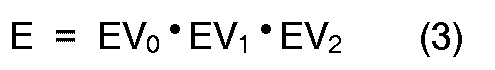

The ANDgate 1110 performs the logical operation of the formula (3) and outputs the coincidence result E. The ANDgates OR gate 1170 cooperate to perform the operation of the formula (4) and to output the Hamming result H. Either of these results is selectively outputted as thesearch result signal 152 by a gate circuit which is composed of the ANDgates OR gate 1180 and -the inverter and is controlled by thereference signal 102. - The searching and processing device shown in Fig. 9 performs successively the logical operations of the formulae (1) and (2) in synchronism with the clock signal 712s, while the searching and processing device of Fig. 11 performs the operations shown in the formulae (3) and (4) in parallel.
- Fig. 12 shows an embodiment of a CAM according to a fourth aspect of the present invention. In the CAM shown in Fig. 7 or in Fig, 10, extension of the bit number of the information being processed is realized by increasing the word number of the
memory 110 or the number ofmemories 110; in the present CAM, the column number or the bit number of thememory 110 is directly increased. For this purpose, the column number of thememory 110 is increased to 2NK and anextended column selector 1210 is introduced. In addition to this feature, acounter 720 for counting input data is coupled to thecolumn selector 1210. - If the present CAM has the memory capacity of N words by M x K bits, the
memory 110 is constructed with a conventional memory cells arranged in a matrix of 2M rows by 2 x N x K columns. That is, thememory 110 has the memory capacity of 2M words by 2 x N x K bits, and the bit number of thecounter 1210 becomes log₂K bits. Thememory 110 is divided into N blocks, each block having 2K columns shown by a broken line, Each block corresponds to one word of the CAM specified by aregistration address 132. Search information and store information of M x K bits are respectively divided into K pieces ofM bit data 101, and are successively inputted in K times in the order of the MSB data piece to the LSB data piece. The store information divided into K pieces ofdatawords 101 is stored as a whole in one block specified by theregistration address 132 in such a manner that each piece of datawords is stored in the corresponding predetermined pair of adjacent columns in the same block, - The store operation and search operation of the CAM shown in Fig. 12 are the same as those for the CAM shown in Fig. 7, except for the following two points: partial datawords of the store information are stored in the direction of column of the
memory 110, and the read-outsignals 151 and 151' based on partial dataword of the search information are obtained by scanning in the direction of column. Thecount output 175 of thecounter 720 is supplied to thecolumn selector 1210 to specify adjacent two columns in each block of thememory 110. The count value of thecounter 720 is incremented for each inputted partial dataword as thedataword 101. Therefore, in the store operation, thecolumn selector 1210 drives an ovencolumn selection line 131 and then the adjacent odd column selection line 131' in a block specified byregistration address 132 for one inputted partial dataword, and repeats such driving operation for every inputted partial dataword while shifing the pair of adjacent even and odd columns to be driven. - In the search operation, on the other hand, the
column selector 1210 drives in parallel the adjacent even and odd twocolumn selection lines 131 and 131' of all the memory blocks specified by thecounter 720 for every inputted partial dataword. Therefore, since thecounter 720 is incremented for each inputted partial data, the pair of adjacent even and odd columns to be driven in each memory block are succesively shifted in the direction of column. In addition, the columns of thememory 110 connected to not-drivencolumn selection lines 131 and 131' are maintained in a high inpedance state, and so, data in only adjacent two columns connected to the column selection lines being driven, are outputted successively to the searching andprocessing device 710 for every inputted partial data of the search information. - As for the
row selector 120, thewrite data generator 140, the search andprocessing device 710 and theencoder 160, the same ones as those used in the CAM shown in Fig. 7 can be employed. - As explained above, a CAM having a memory capacity of N words by M x k bits can be constructed using a conventional memory of 2M words by 2Nk bits. In view of the fact that the CAM shown in Fig. 1 requires a conventional memory of 2Mxk words by 2N bits for the purpose of having the same memory capacity, the present CAM can be constructed with a memory of a smaller memory capacity, and therefore, is very inexpensive. It is another advantage that the CAM is also capable of carrying out the search operation for data having the
Hamming distance 1 from the search information as well as search operation for data identical with the search information. - Fig. 13 shows an embodiment of the
column selector 1210 used in the CAM shown in Fig. 12. This column selector comprises ablock decoder 1310 receiving theregistration address 132, and acolumn decoder 1320 receiving the output from thecounter 720. Theblock decoder 1310 includes a plurality of parallel output lines and operates to selectively drive one of the associated output lines designated by theregistration address 132. The output lines of theblock decoder 1310 are respectively connected in one-to-one relation to one inputs of two-input OR gates which are arranged in parallel to form anOR gate array 1340. The other input of each OR gate in thegate array 1340 is supplied with theoperation mode signal 103 via an inverter 1330, and outputs of all the OR gates are connected in one-to-one relation to ANDgate arrays 1380, each of which is associated to one of the memory blocks. On the other hand, thecolumn decoder 1320 comprises a plurality of parallel output lines and selectively drives one of the associated output lines specified by thecount output 175 of thecounter 720. In addition, each output of thecolumn decoder 1320 is supplied to all the ANDgate arrays 1380. Further, the output of the inverter 1330 is connected to one inputs of two ORgates OR gates 1360 is connected at its other input to an output of anotherinverter 1350 receiving thecolumn selection signal 133, and the other input of the other ORgate 1370 is connected to directly receive thecolumn selection signal 133. Outputs of the two ORgates gate arrays 1380. - Each of the AND
gate arrays 1380 comprises parallel arranged three-input AND gates of two times the number of the output lines of thecolumn decoder 1320. In each AND gate array, first inputs of all the AND gates are connected to the output of the corresponding one OR gate in theOR gate array 1340. Each pair of adjacent AND gates are connected at their second input in common to one corresponding output line of thecolumn decoder 1320. One AND gate of each AND gate pair, i.e., each even-numbered AND gate has a third input connected to the output of theOR gate 1360 and an output connected to an evencolumn selection line 131. The other AND gate of each AND gate pair, i.e., each odd-numbered AND gate is connected at its third input to the output of theOR gate 1370 and at its output to an odd column selection line 131'. - In the search operation, since "0" is applied as the
operation mode signal 103, "1" is outputted from theOR gates column selection lines 131 and 131' coupled to each block of thememory 110 specified by thecolumn decoder 1320 are driven in parallel. - In the store operation, "1" is applied as the
operation mode signal 103. Therefore, theblock decoder 1310 selects one of the ANDgate arrays 1380 on the basis of theregistration address 132, and thecolumn decoder 1320 further selects one pair of the pairs of adjacent AND gates in the designated AND gate array in accordance with by thecount output 175 of thecounter 720. The ORgates column selection signal 133, so that the even and oddcolumn selection lines 131 and 131' respectively connected to the outputs of the selected pair of adjacent AND gates are selectively and sequentially driven in the mentioned order. Thus, it is allowed to write data in one pair of columns in the memory connected to the pair of even and oddcolumn selection lines 131 and 131' so driven. - Fig. 14 shows an embodiment of a CAM according to a fifth of the present invention. The present CAM, aiming at large memory capacity, comprises a plurality of CAM unite 1410 corresponding to the CAM shown in Figs. 1, 7, 10 and 12, a plurality of
data outputting device 1420 receiving data from the plurality ofCAM units 1410, anencoder 1430 receiving data from the plurality ofdata outputting devices 1420 and adecoder 1440 for applyingwrite timing pulses 104 to eachCAM unit 1410. Theclock signal 712, thereference signal 102, theinitial setting signal 711, theinput data 101, theoperation mode signal 103, theregistration address 132 and thecolumn selection signal 133 are applied in parallel to all theCAM units 1410. - The present CAM is capable of processing multiple matching when a plurality of information specified by the search information under the condition of the reference signal are stored in the memory. In the following, explanation will be mode on multiple matching processing. In order to use the CAMs shown in Figs, 1, 7 and 12 as a
CAM unit 1410, a few components must be further equipped to the CAMs. The CAM shown in Fig. 1 must be equipped with a register receiving thesearch result signal 152. Further, the CAMs shown in Figs. 1, 7 and 12 must be equipped with a decoder receiving thesearch address 162 and applying a reset signal to the register or the searching andprocessing device 710 specified by the search address. In multiple matching operation, if the reset signal is applied from the decoder to the register or to the searching and processing device, thesearch result signal 152 corresponding to thesearch address 162 so far outputted is cleared. As a result, theencoder 162 generates thenext search address 162, enabling multiple matching processing. The CAM capable of processing multiple matching of data as explained above is used as eachCAM unit 1410. - In the store operation, the
operation mode signal 103 of "1", theinitial setting signal 711, thecolumn signal 133, theclock signal 712, theinput data 101 and theregistration address 132 are applied to eachCAM unit 1410, similarly to the CAM shown in Figs. 1, 7, 10 and 12. The registration address is divided into a loworder resistration address 132 and a high order registration address 1441: the former is supplied to each CAM units and the latter is applied to thedecoder 1440. The highorder registration address 1441 specifies one of theCAM units 1410, while theregistration address 132 specifies words in theCAM unite 1410. Awrite signal 1442 instructing the write operation of data to the CAM is applied to thedecoder 1440, which then selectively applies thewrite timing signal 104 to theCAM unit 1410 specified by the highorder registration address 1441. By means of thedecoder 1440, information is stored in the CAM unit specified by the highorder registration address 1441. - In the search operation, the
clock signal 712, thereference signal 102, theinitial setting signal 711, theinput data 101 and theoperation mode signal 103 are applied in parallel to eachCAM unit 1410. From theCAM units 1410 storing the data specified by the search information (input data) 101 under the condition of thereference signal 102, thecoincidence signal 161 of "1" is outputed together with thesearch address 162. When "1" is outputed as the coincidence signal 161 from a plurality ofCAM units 1410, the CAM units are given a priority order from right to left, so that thedata outputting device 1420 outputs thesearch address 162 in the order from highorder CAM unit 1410. In order to establish such a priority order of CAM units, an enablesignal 1422 of "1" is applied to thedata outputting device 1420 of the highest order Or the leftmost CAM unit and at the same time eachdata outputting device 1420 supplies an enable signal to the adjacent right-side data outputting device. When thedata outputting device 1420 receives the enable signal of "1", if it also receives thecoincidence signal 161 of "1", it operated to output thesearch address 162 to an address bus 1421 and at the same time supplies an enable signal of "0" to the adjacent Left-sidedata output device 1420. But, if thedata outputting device 1420 receives the coincidence signal of "0" when it receives the enable signal of "1", it supplies the enable signal of "1" to the adjacent right-sidedata output device 1420. Further, if thedata outputting device 1420 receives the enable signal of "0", it operates to put an internal output buffer for the search address in a high impedance state, irrespectively of the condition of thecoincidence signal 161, and at the same time to supply the enable signal of "0" to the right-side device. Therefore, all the data outputting devices positioned at the right of the data outputting device which supplies thesearch address 162 to the bus 1421, maintain their internal output buffer in a high impedance state. - Further, the
data outputting device 1420, outputting thesearch address 162, also outputs thecoincidence signal 161 of "1" as thefirst coincidence signal 1423 to theencoder 1430, while, all thedata outputting devices 1420 excluding thedata outputting device 1420 outputting the search address, generate thefirst coincidence signal 1423 of "0" to theencoder 1430. Theencoder 1430, receiving these first coincidence signals 1423, generates asecond coincidence signal 1431 indicating whether or not "1" is inputted as thefirst coincidence signal 1423, and also produces a highorder search address 1432 indicating the location of thefirst coincidence signal 1423 of "1". Thesecond coincidence signal 1431 indicates that the data specified by the search information under the condition of the reference signal is stored in the CAM. The highorder search address 1432 indicates the location of the CAM unit where the desired data is stored. The low order search address 1421 indicates thesearch address 162 of the CAM unit, that is, the position of column of the memory storing the desired data. - External apparatus (not shown) watches the
second coincidence signal 1431, and reads the highorder search address 1432 and the low order search address 1421, and also applies afirst reset signal 1424 to eachdata outputting device 1420. Thefirst reset signal 1424 makes it possible to obtain the the search address corresponding to the next higher priority order information when a plurality of information identical with the search information are stored in the CAM. Thedata outputting device 1420, outputting thesearch address 162, responds to thefirst reset signal 1424 to supply areset signal 1031 to the associatedCAM unite 1410, so that it outputs thenext search address 162. - As explained above, the present CAM can be constructed with the CAMs shown in Figs. 1, 7, 10 and 12. Therefore, extension of the word number is easily realized to provide a large memory capacity CAM.
- Fig. 15 is an illustration of the
data outputting device 1420 used in the CAM shown in Fig. 14. The data outputting device comprises an output buffer 1510, three ANDgates inverter 1550, which are connected as shown. - When both the
coincidence signal 161 and the enablesignal 1422 inputted to an enablesignal input terminal 1560 from the left sidedata outputting device 1420 are "1", the ANDgate 1530 outputs a signal of "1" as thefirst coincidence signal 1423, and controls the output buffer 1510 so that thesearch address 162 is outputted through the output buffer 1510 as the low order search address 1421. Further, the ANDgate 1540 outputs the enable signal of "0" to an enablesignal output terminal 1570, which will be connected to the enable signal input terminal of the right sidedata outputting device 1420. Therefore, the output buffer 1510 of theright side device 1420 is brought into a high impedence state. Further, thefirst reset signal 1424 passes through the ANDgate 1520 and is applied asreset signal 1031 to the associated CAM unit. In all thedata outputting device 1420 located at the each side of thedata outputting device 1420 generating "1" as thefirst coincidence signal 1423, thefirst reset signal 1424 does not pass through the ANDgate 1520 and therefore does not output thereset signal 1031. - As explained in detail so far, a CAM according to the present invention can be constructed with inexpensive conventional memory devices accessed by applying the address indicating the location of desired dataword. The CAM shown in Fig. 1 having a memory capacity of N words by M bits can be constructed by using a conventional memory of 2M words by 2N bits as the
memory 110. The CAMs shown in Figs. 7, 10 and 12 having a memory capacity of N words by M x K bits can be constructed with a conventional memory of 2M x K words by 2N bits or 2M words by 2NK bits or with K pieces of conventional memories having 2M words by 2N bits. Therefore, using a 1 Mbit memory chip, the following CAMs can be constructed with only one chip: a CAM having 512 words by 10 bits as shown in Fig. 1 or, supposing theinput data 101 of 6 bits and the search information divided into eight pieces (k=8), a 48 kilo-bits CAM with 1 kilo-words by 48 bits as shown in Figs. 7, 10 and 12. Examining CAMs available in the market, for example, CAM "IC 8220" commercially available from Signetics Corporation has a memory capacity of 4 words by 2 bits. Therefore, it is apparent that a CAM according to the present invention has a remarkably large memory capacity. - Search operation and store operation in the CAM can be performed only with one or a few accesses to a conventional memory. Therefore, the operation of the CAM can be executed at a speed higher than those realized in the conventional CAM of the word-serial/bit-parallel type and the word-parallel/bit-serial type. Further, it is possible to carry out the search operation by masking a part of search information, and also to perform the multiple matching processing when desired data are stored in a plurality of addresses. Extension of the memory capacity can be also easily realized, Not only search operation by under the coincidence condition but also search operation within a specified Hamming distance can be performed.
- In summary, according to the present invention, a high operation speed, large memory capacity, low priced, multiple function CAM can be realized. If such a CAM is applied to a memory of an information processing system such as data base, pattern recognition and artificial intelligence, the system can perform a high speed associative processing and comparison operation.
- In the embodiments mentioned hereinbefore, for even number columns of the
memory 110, "1" is stored only in one row specified by the store information, and for odd number columns of thememory 110, "1" is stored in rows specified by datawords having Hamming distance "1" from the store information. This is only an example of dataword store. There are many other methods of storing datawords. As for Hamming distance, a variety of distances can be chosen. For example, "1" can be stored in rows specified by all data within a predetermined Hamming distance. Datawords of different Hamming distances may be stored in a plurality of columns in such a manner that all the datawords the same Hamming distance are stored in the same column. Further, Hamming distance can be specified at the beginning of store operation. In the above embodiments, information is stored in one pair of adjacent columns of thememory 110, but the two columns need not to be adjacent each other, As explained above, changes and modifications are also possible for thewrite data generater 140, the searching andprocessing device 710 and thecolumn selections 130end 1210. - The number of input/output terminals can be reduced by using the same terminals for the
registration address bus 132 and thesearch address bus 162. - Therefore, the inventions are in no way limited to details of the illustrated structures.
Claims (10)
- A content-addressable memory device for searching datawords and their associated addresses j, said memory device storing N datawords, all said datawords consisting of k or m pieces, whereby each piece consists of M bits with k, m = 1, 2, ... n, and has its data coded in an "1 of M" code; and every dataword having its associated address j, said content-addressable memory device comprising:
memory means (110) including a matrix of conventional memory cells of k x 2M rows by m x N pairs of columns, wherein each dataword (101) is stored in said m pairs of columns corresponding to its associated address j (162) and whereby in every first column of a said pair the dataword (101) itself is stored, while in the other column a dataword having a certain functional relation to said dataword (101) is stored;
row selecting means (120) coupled to said memory means (110) adapted to, in the case of a search operation, sequentially selecting all k rows of said matrix of memory cells corresponding to the k "1 of M" codes;
column selecting means (130) coupled to said memory means (110) adapted to, in the case of a store operation, sequentially selecting all m pairs of columns of said matrix of memory cells corresponding to the datawords address j (162);
an encoder (160) adapted to, in the case of search operation, receiving row by row all data that is stored in the memory cells of said k selected rows and coding from the therein activated m columns the required search address j. - A content-addressable memory device as claimed in claim 1, further comprising:
switching means (150) including a plurality of switches (153) each having a pair of inputs coupled respectively with the first column and the second column of the same pair of columns in the matrix of said memory means (110) so as to receive respectively the content of the memory cell of the first and second columns of each pair belonging to the row selected by the row selecting means (120), and adapted to output the content of the memory cell of at least one column of the first and second columns of each pair belonging to the row selected by the row selecting means (120); and wherein said
encoder (160) receives the output of the switching means (150) and encodes it to an address j (162) at least one of the search datawords and the data associated therewith. - A content-addressable memory device as claimed in claim 2, wherein the row selecting means (120) comprises a decoder (410) receiving the dataword (101) and outputting a signal representing the row of the matrix of said memory means (110) corresponding to the content of said dataword (101).
- A content-addressable memory device as claimed in claim 1, further comprising:
data writing means (140) for writing the dataword (101) in the first column of the pair of columns of said matrix selected by the column selecting means (130) and the data associated to said dataword in the second column of the pair of columns selected by the column selecting means (130). - A content-addressable memory device as claimed in claim 4, wherein the row selecting means comprises:
a decoder (410) receiving dataword (101) being searched or stored and decoding the dataword to signals corresponding to the row of the memory cell matrix and representing the row position of the memory cell matrix corresponding to the content of said dataword; and
a number of OR gates (420) each having two inputs receiving respectively one of the decoded signals and an operation mode signal indicating the store operation or search operation. - A content-addressable memory device as claimed in claim 5, wherein the decoded signal corresponding to the row position of the matrix which corresponds to the content of the dataword is "1", while the other decoded signals are "0", and the operation mode signal (103) is "1" when the store operation is ordered, while it is "0" when the search operation is ordered.
- A content-addressable memory device as claimed in claim 4, wherein the column selecting means (130) comprises
a decoder (510) means receiving the address j (162) and outputting a signal representing the position of the pair of columns of the matrix of the memory means (110) which corresponds to the adress j. - A content-addressable memory device as claimed in claim 7, wherein the column selecting means (130) decodes the input address so as to output, in response to a column selection signal (133), a signal corresponding to the first or second column of the pair of columns in the memory cell matrix which corresponds to the input address.
- A content-addressable memory device as claimed in claim 4, wherein the column selecting means comprises:
a decoder (510) receiving the address j as the upper order signal and a column selection signal (133) as the least significant signal and decoding these signals to signals representing the first or second columns of the pairs of columns corresponding to the address j in accordance with the variation of the column selection signal (133) and a plurality of OR gates (520) each corresponding to the columns of the memory cells of the memory means (110) and receiving the corresponding decoded signal and an inverted operation mode signal. - A content-addressable memory devices as claimed in claim 9, wherein the decoded signals representing the first or second column of the pair of the columns of the matrix corresponding to the address j is "1", while the other decoded signals are "0", and the operation mode signal (103) is "1" when the store operation is ordered, while it is "0" when the search operation is ordered.
Applications Claiming Priority (2)
| Application Number | Priority Date | Filing Date | Title |
|---|---|---|---|
| JP59229512A JPS61107596A (en) | 1984-10-31 | 1984-10-31 | Associative memory |
| JP229512/84 | 1984-10-31 |
Publications (3)
| Publication Number | Publication Date |
|---|---|
| EP0180239A2 EP0180239A2 (en) | 1986-05-07 |
| EP0180239A3 EP0180239A3 (en) | 1989-03-22 |
| EP0180239B1 true EP0180239B1 (en) | 1993-03-03 |
Family
ID=16893334
Family Applications (1)
| Application Number | Title | Priority Date | Filing Date |
|---|---|---|---|
| EP85113907A Expired - Lifetime EP0180239B1 (en) | 1984-10-31 | 1985-10-31 | Content-addressable memory |
Country Status (4)
| Country | Link |
|---|---|
| US (1) | US4755974A (en) |
| EP (1) | EP0180239B1 (en) |
| JP (1) | JPS61107596A (en) |
| DE (1) | DE3587137T2 (en) |
Families Citing this family (37)
| Publication number | Priority date | Publication date | Assignee | Title |
|---|---|---|---|---|
| JPS61145636A (en) * | 1984-12-19 | 1986-07-03 | Nec Corp | Symbol string collating device |
| US4959811A (en) * | 1986-11-03 | 1990-09-25 | Texas Instruments Incorporated | Content addressable memory including comparison inhibit and shift register circuits |
| US5122984A (en) * | 1987-01-07 | 1992-06-16 | Bernard Strehler | Parallel associative memory system |
| JPH0673114B2 (en) * | 1987-03-31 | 1994-09-14 | 日本電気株式会社 | Cash controller |
| JP2714944B2 (en) * | 1987-08-05 | 1998-02-16 | 三菱電機株式会社 | Semiconductor storage device |
| US5146456A (en) * | 1988-04-08 | 1992-09-08 | Allied-Signal Inc. | Computer system with distributed content-addressable memory modules compatible with cito transmission |
| US5142676A (en) * | 1988-12-28 | 1992-08-25 | Gte Laboratories Incorporated | Separate content addressable memories for storing locked segment addresses and locking processor identifications for controlling access to shared memory |
| US5053991A (en) * | 1989-10-06 | 1991-10-01 | Sanders Associates, Inc. | Content-addressable memory with soft-match capability |
| US5063521A (en) * | 1989-11-03 | 1991-11-05 | Motorola, Inc. | Neuram: neural network with ram |
| SE9002558D0 (en) * | 1990-08-02 | 1990-08-02 | Carlstedt Elektronik Ab | PROCESSOR |
| US5220526A (en) * | 1991-03-01 | 1993-06-15 | Motorola, Inc. | Method and apparatus for indicating a duplication of entries in a content addressable storage device |
| US5182802A (en) * | 1992-04-06 | 1993-01-26 | Dillard Lawrence D | Data addressable memory architecture and method of forming a data addressable memory |
| GB9213821D0 (en) * | 1992-06-30 | 1992-08-12 | Inmos Ltd | Content addressable memory |
| US6005811A (en) * | 1994-08-17 | 1999-12-21 | Oak Technology, Incorporated | Method for operating a memory |
| FR2736737B1 (en) * | 1995-07-12 | 1997-08-14 | Alcatel Nv | DEVICE FOR MANAGING RELATIONSHIPS BETWEEN OBJECTS |
| US6661421B1 (en) | 1998-05-21 | 2003-12-09 | Mitsubishi Electric & Electronics Usa, Inc. | Methods for operation of semiconductor memory |
| US6559851B1 (en) | 1998-05-21 | 2003-05-06 | Mitsubishi Electric & Electronics Usa, Inc. | Methods for semiconductor systems for graphics processing |
| US6535218B1 (en) | 1998-05-21 | 2003-03-18 | Mitsubishi Electric & Electronics Usa, Inc. | Frame buffer memory for graphic processing |
| US6504550B1 (en) | 1998-05-21 | 2003-01-07 | Mitsubishi Electric & Electronics Usa, Inc. | System for graphics processing employing semiconductor device |
| US6711558B1 (en) | 2000-04-07 | 2004-03-23 | Washington University | Associative database scanning and information retrieval |
| ATE435492T1 (en) * | 2000-11-21 | 2009-07-15 | Aspex Technology Ltd | IMPROVEMENTS TO CONTENT ADDRESSABLE STORAGE ARRANGEMENTS |
| US7216284B2 (en) * | 2002-05-15 | 2007-05-08 | International Business Machines Corp. | Content addressable memory having reduced power consumption |
| JP2004334295A (en) * | 2003-04-30 | 2004-11-25 | Yamaha Corp | Storage device |
| CA2759064C (en) | 2003-05-23 | 2017-04-04 | Washington University | Intellegent data storage and processing using fpga devices |
| US10572824B2 (en) | 2003-05-23 | 2020-02-25 | Ip Reservoir, Llc | System and method for low latency multi-functional pipeline with correlation logic and selectively activated/deactivated pipelined data processing engines |
| JP4346975B2 (en) * | 2003-06-27 | 2009-10-21 | 株式会社ルネサステクノロジ | Integrated circuit with content addressable memory function and intrusion detection device |
| JP2005353107A (en) * | 2004-06-08 | 2005-12-22 | Hitachi Ltd | Semiconductor device |
| CA2599382A1 (en) | 2005-03-03 | 2006-09-14 | Washington University | Method and apparatus for performing biosequence similarity searching |
| JP4643315B2 (en) * | 2005-03-11 | 2011-03-02 | 株式会社東芝 | Semiconductor integrated circuit device |
| US7571371B2 (en) * | 2005-08-18 | 2009-08-04 | Hewlett-Packard Development Company, L.P. | Parallel parity checking for content addressable memory and ternary content addressable memory |
| JP2007148779A (en) * | 2005-11-28 | 2007-06-14 | Renesas Technology Corp | Microcontroller and ram |
| US7660793B2 (en) | 2006-11-13 | 2010-02-09 | Exegy Incorporated | Method and system for high performance integration, processing and searching of structured and unstructured data using coprocessors |
| US8326819B2 (en) | 2006-11-13 | 2012-12-04 | Exegy Incorporated | Method and system for high performance data metatagging and data indexing using coprocessors |
| KR101095799B1 (en) * | 2009-05-29 | 2011-12-21 | 주식회사 하이닉스반도체 | Cam cell circuit of nonvolatile memory device and driving method thereof |
| EP3560135A4 (en) | 2016-12-22 | 2020-08-05 | IP Reservoir, LLC | LEARNING PIPING FOR HARDWARE ACCELERATED MACHINERY |
| US10572440B2 (en) * | 2017-12-21 | 2020-02-25 | Stmicroelectronics International N.V. | High operation frequency, area efficient and cost effective content addressable memory architecture |
| US11262913B2 (en) * | 2019-03-28 | 2022-03-01 | Intel Corporation | Technologies for efficient stochastic associative search operations with error-correcting code |
Family Cites Families (3)
| Publication number | Priority date | Publication date | Assignee | Title |
|---|---|---|---|---|
| US3644906A (en) * | 1969-12-24 | 1972-02-22 | Ibm | Hybrid associative memory |
| US3699545A (en) * | 1971-02-24 | 1972-10-17 | Northern Electric Co | Adaptable associative memory system |
| US4045781A (en) * | 1976-02-13 | 1977-08-30 | Digital Equipment Corporation | Memory module with selectable byte addressing for digital data processing system |
-
1984
- 1984-10-31 JP JP59229512A patent/JPS61107596A/en active Granted
-
1985
- 1985-10-31 DE DE8585113907T patent/DE3587137T2/en not_active Expired - Fee Related
- 1985-10-31 EP EP85113907A patent/EP0180239B1/en not_active Expired - Lifetime
- 1985-10-31 US US06/793,388 patent/US4755974A/en not_active Expired - Fee Related
Also Published As
| Publication number | Publication date |
|---|---|
| JPS61107596A (en) | 1986-05-26 |
| EP0180239A2 (en) | 1986-05-07 |
| JPH0519238B2 (en) | 1993-03-16 |
| DE3587137T2 (en) | 1993-09-09 |
| US4755974A (en) | 1988-07-05 |
| DE3587137D1 (en) | 1993-04-08 |
| EP0180239A3 (en) | 1989-03-22 |
Similar Documents
| Publication | Publication Date | Title |
|---|---|---|
| EP0180239B1 (en) | Content-addressable memory | |
| US4907194A (en) | String comparator for searching for reference character string of arbitrary length | |
| US4314356A (en) | High-speed term searcher | |
| US4660181A (en) | Memory system | |
| US4170039A (en) | Virtual address translation speed up technique | |
| US6760821B2 (en) | Memory engine for the inspection and manipulation of data | |
| US4095283A (en) | First in-first out memory array containing special bits for replacement addressing | |
| WO1993025975A2 (en) | A programmable logic device | |
| EP0086992B1 (en) | Microword generation mechanism utilizing separate programmable logic arrays | |
| US4679167A (en) | Apparatus for locating a memory module within a memory space | |
| US4128872A (en) | High speed data shifter array | |
| US3389377A (en) | Content addressable memories | |
| US4006470A (en) | Read-only memory | |
| US4510617A (en) | Character recognition system utilizing pattern matching method | |
| WO1988001411A1 (en) | A content-addressable memory system | |
| US4777622A (en) | Associative data storage system | |
| US5524226A (en) | Register file system for microcomputer including a decoding system for concurrently activating source and destination word lines | |
| US5055717A (en) | Data selector circuit and method of selecting format of data output from plural registers | |
| RU2092912C1 (en) | Memory unit which has commutation structure | |
| RU2028664C1 (en) | Concurrent data processing device | |
| JPH024926B2 (en) | ||
| SU809206A1 (en) | Device for searching data in memory | |
| SU1656543A1 (en) | Device for memory addressing | |
| SU1049974A1 (en) | Information retrieval unit for associative memory | |
| SU1278842A1 (en) | Random markovian process generator |
Legal Events
| Date | Code | Title | Description |
|---|---|---|---|
| PUAI | Public reference made under article 153(3) epc to a published international application that has entered the european phase |
Free format text: ORIGINAL CODE: 0009012 |
|
| 17P | Request for examination filed |
Effective date: 19851129 |
|
| AK | Designated contracting states |
Kind code of ref document: A2 Designated state(s): DE FR GB |
|
| PUAL | Search report despatched |
Free format text: ORIGINAL CODE: 0009013 |
|
| RHK1 | Main classification (correction) |
Ipc: G06F 15/40 |
|
| AK | Designated contracting states |
Kind code of ref document: A3 Designated state(s): DE FR GB |
|
| 17Q | First examination report despatched |
Effective date: 19911121 |
|
| GRAA | (expected) grant |
Free format text: ORIGINAL CODE: 0009210 |
|
| AK | Designated contracting states |
Kind code of ref document: B1 Designated state(s): DE FR GB |
|
| REF | Corresponds to: |
Ref document number: 3587137 Country of ref document: DE Date of ref document: 19930408 |
|
| ET | Fr: translation filed | ||
| PLBE | No opposition filed within time limit |
Free format text: ORIGINAL CODE: 0009261 |
|
| STAA | Information on the status of an ep patent application or granted ep patent |
Free format text: STATUS: NO OPPOSITION FILED WITHIN TIME LIMIT |
|
| 26N | No opposition filed | ||
| PGFP | Annual fee paid to national office [announced via postgrant information from national office to epo] |
Ref country code: FR Payment date: 19951027 Year of fee payment: 11 |
|
| PGFP | Annual fee paid to national office [announced via postgrant information from national office to epo] |
Ref country code: GB Payment date: 19951030 Year of fee payment: 11 |
|
| PGFP | Annual fee paid to national office [announced via postgrant information from national office to epo] |
Ref country code: DE Payment date: 19951219 Year of fee payment: 11 |
|
| PG25 | Lapsed in a contracting state [announced via postgrant information from national office to epo] |
Ref country code: GB Effective date: 19961031 |
|
| GBPC | Gb: european patent ceased through non-payment of renewal fee |
Effective date: 19961031 |
|
| PG25 | Lapsed in a contracting state [announced via postgrant information from national office to epo] |
Ref country code: FR Effective date: 19970630 |
|
| PG25 | Lapsed in a contracting state [announced via postgrant information from national office to epo] |
Ref country code: DE Effective date: 19970701 |
|
| REG | Reference to a national code |
Ref country code: FR Ref legal event code: ST |