EP0180153B1 - Digital crystal-stable fm discriminator - Google Patents
Digital crystal-stable fm discriminator Download PDFInfo
- Publication number
- EP0180153B1 EP0180153B1 EP85113542A EP85113542A EP0180153B1 EP 0180153 B1 EP0180153 B1 EP 0180153B1 EP 85113542 A EP85113542 A EP 85113542A EP 85113542 A EP85113542 A EP 85113542A EP 0180153 B1 EP0180153 B1 EP 0180153B1
- Authority
- EP
- European Patent Office
- Prior art keywords
- phase comparator
- discriminator
- signal
- frequency
- output signal
- Prior art date
- Legal status (The legal status is an assumption and is not a legal conclusion. Google has not performed a legal analysis and makes no representation as to the accuracy of the status listed.)
- Expired
Links
Images
Classifications
-
- H—ELECTRICITY
- H03—ELECTRONIC CIRCUITRY
- H03D—DEMODULATION OR TRANSFERENCE OF MODULATION FROM ONE CARRIER TO ANOTHER
- H03D3/00—Demodulation of angle-, frequency- or phase- modulated oscillations
- H03D3/02—Demodulation of angle-, frequency- or phase- modulated oscillations by detecting phase difference between two signals obtained from input signal
- H03D3/24—Modifications of demodulators to reject or remove amplitude variations by means of locked-in oscillator circuits
- H03D3/241—Modifications of demodulators to reject or remove amplitude variations by means of locked-in oscillator circuits the oscillator being part of a phase locked loop
Definitions
- the invention relates to a digital quartz-stable FM discriminator with a phase locked loop (PLL: Phase Locked Loop), which contains a phase comparator and a switchable frequency divider, in which the phase comparator has the input signal of the discriminator and the output signal of the frequency divider and the frequency divider a quartz-stable frequency and the output signal of the phase comparator are supplied.
- PLL Phase Locked Loop
- Such a circuit arrangement is essentially known from US-A-3 983 498.
- PLL phase locked loop demodulators
- VCO Voltage controlled oscillator
- the characteristic curve of the VCO corresponds to the demodulator characteristic curve, which means that non-linearities result in a distortion factor.
- VCO When the VCO is controlled without a low pass, a digital two-point controller results.
- the VCO generates only two frequencies, which correspond to the lowest and highest demodulable frequency.
- the duty cycle corresponds to the ratio of the input frequency to the two possible VCO frequencies.
- the invention has for its object to provide an FM discriminator that is as linear, temperature independent and frequency stable as possible.
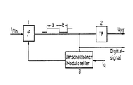
- the figure shows the FM discriminator in the block diagram.
- the input signal of the frequency f A is supplied to a phase comparator. 1 This is followed by a low pass 2, the output of which the voltage U NF (low frequency signal) can be taken.
- a PLL loop is switched on from the signal path between phase comparator 1 and low pass 2 to a further input of phase comparator 1.
- the switchable modulo divider 3 generates the two corner frequencies f u and f o of the FM discriminator by switching.
- the low frequency signal (U NF ) appears after this.
- the frequencies f o and f u generated by the modulo divider 3 are only dependent on the quartz frequency fq, that is to say quartz-stable. It is therefore not necessary to adjust the circuit.
- the pulse duty factor can be counted very advantageously at this point and thus digitized.
- the digital signal in front of the modulo divider 3 is extracted within the circuit.
Abstract
Description
Die Erfindung bezieht sich auf einen digitalen quarzstabilen FM-Diskriminator mit einer Phasenregelschleife (PLL: Phase Locked Loop), die einen Phasenvergleicher und einen umschaltbaren Frequenzteiler enthält, bei dem dem Phasenvergleicher das Eingangssignal des Diskriminators und das Ausgangssignal des Frequenzteilers und dem Frequenzteiler eine quarzstabile Frequenz und das Ausgangssignal des Phasenvergleichers zugeführt werden. Eine solche Schaltungsanordnung ist im wesentlichen aus der US-A-3 983 498 bekannt.The invention relates to a digital quartz-stable FM discriminator with a phase locked loop (PLL: Phase Locked Loop), which contains a phase comparator and a switchable frequency divider, in which the phase comparator has the input signal of the discriminator and the output signal of the frequency divider and the frequency divider a quartz-stable frequency and the output signal of the phase comparator are supplied. Such a circuit arrangement is essentially known from US-A-3 983 498.
PLL (Phase Locked Loop)-Demodulatoren, die in üblicher Weise einen VCO (Voltage controlled oscillator) über einen Tiefpass so nachregeln, dass die VCO-Frequenz gleich der Eingangsfrequenz ist, wobei die Regelspannung am VCO der NF-Spannung entspricht, haben den Nachteil, dass die VCO's wegen ihrer Temperatur- und Spannungsabhängigkeit nur schwer zu stabilisieren sind. Dies macht es erforderlich, dass der VCO abgeglichen werden muss. Die Kennlinie des VCO entspricht der Demodulatorkennlinie, was bedeutet, dass Unlinearitäten einen Klirrfaktor ergeben.PLL (phase locked loop) demodulators, which regulate a VCO (Voltage controlled oscillator) via a low pass in the usual way so that the VCO frequency is equal to the input frequency, whereby the control voltage at the VCO corresponds to the LF voltage, have the disadvantage that the VCOs are difficult to stabilize due to their temperature and voltage dependency. This requires the VCO to be matched. The characteristic curve of the VCO corresponds to the demodulator characteristic curve, which means that non-linearities result in a distortion factor.
Bei Ansteuerung des VCO ohne Tiefpass ergibt sich ein digitaler Zweipunktregler. Der VCO erzeugt nur zwei Frequenzen, die der niedrigsten und höchsten demodulierbaren Frequenz entsprechen. Das Tastverhältnis entspricht dem Verhältnis der Eingangsfrequenz zu den beiden möglichen VCO-Frequenzen.When the VCO is controlled without a low pass, a digital two-point controller results. The VCO generates only two frequencies, which correspond to the lowest and highest demodulable frequency. The duty cycle corresponds to the ratio of the input frequency to the two possible VCO frequencies.
Der Erfindung liegt die Aufgabe zugrunde, einen FM-Diskriminator zu schaffen, der möglichst linear, temperaturunabhängig und frequenzstabil ist.The invention has for its object to provide an FM discriminator that is as linear, temperature independent and frequency stable as possible.
Diese Aufgabe wird für einen FM-Diskriminator der eingangs beschriebenen Art gemäss der Erfindung in der Weise gelöst, dass im Signal- übertragungsweg am Verbindungspunkt vom Ausgang des Phasenvergleichers und Eingang des Frequenzteilers ein Tiefpass eingeschaltet ist, dem das Ausgangssignal des Phasenvergleichers zugeführt wird und dessen Ausgang eine Spannung UNI entnehmbar ist, dass der Frequenzteiler durch Umschalten ein Signal erzeugt, das die Eckfrequenzen fu und fo des Diskriminators enthält und dass die Frequenz des Eingangssignals fEin = a fo+b fu ist, wobei a+b = 1 ist und a und b das Tastverhältnis des dem Frequenzteiler als Steuersignal zugeführten Ausgangssignals des Phasenvergleichers angeben.This object is achieved for an FM discriminator of the type described at the outset according to the invention in such a way that a low-pass filter is switched on in the signal transmission path at the connection point from the output of the phase comparator and input of the frequency divider, to which the output signal of the phase comparator and its output are fed a voltage U NI can be seen that the frequency divider generates a signal by switching, which contains the corner frequencies f u and f o of the discriminator and that the frequency of the input signal f Ein = af o + b fu, where a + b = 1 and a and b indicate the duty cycle of the output signal of the phase comparator supplied to the frequency divider as a control signal.
Nachstehend wird die Erfindung anhand eines in der Zeichnung dargestellten Ausführungsbeispiels näher erläutert.The invention is explained in more detail below on the basis of an exemplary embodiment shown in the drawing.
Die Figur zeigt den FM-Diskriminator im Blockschaltbild. Das Eingangssignal der Frequenz fEin wird einem Phasenvergleicher 1 zugeführt. Diesem ist ein Tiefpass 2 nachgeschaltet, dessen Ausgang die Spannung UNF (Niederfrequenzsignal) entnehmbar ist. Vom Signalweg zwischen Phasenvergleicher 1 und Tiefpass 2 ist eine PLL-Schleife zu einem weiteren Eingang des Phasenvergleichers 1 eingeschaltet. Diese enthält einen umschaltbaren Moduloteiler 3, dem eine quarzstabile Frequenz fq zugeführt wird. Der umschaltbare Moduloteiler 3 erzeugt durch Umschalten die beiden Eckfrequenzen fu und fo des FM-Diskriminators.The figure shows the FM discriminator in the block diagram. The input signal of the frequency f A is supplied to a phase comparator. 1 This is followed by a
Es ergibt sich fEin = a fo+b fu, wobei a+b = 1 ist und a und b das Tastverhältnis des dem Frequenzteiler 3 als Steuersignal zugeführten Ausgangssignals des Phasenvergleichers 1 angeben.The result is f specify A = af + bf o u, where a + b = 1 and a and b are the duty ratio of the
Schickt man das Steuersignal durch den Tiefpass 2, so erscheint nach diesem das Niederfrequenzsignal (UNF). Die durch den Moduloteiler 3 erzeugten Frequenzen fo und fu sind nur von der Quarzfrequenz fq abhängig, also quarzstabil. Ein Abgleich der Schaltung ist also nicht erforderlich.If you send the control signal through the
Da am Tiefpass ein Tastverhältnis anliegt, kann an dieser Stelle sehr vorteilhaft das Tastverhältnis ausgezählt und so digitalisiert werden. Innerhalb der Schaltung wird das Digitalsignal vor dem Moduloteiler 3 entnommen.Since there is a pulse duty factor at the low-pass filter, the pulse duty factor can be counted very advantageously at this point and thus digitized. The digital signal in front of the
Claims (1)
Priority Applications (1)
| Application Number | Priority Date | Filing Date | Title |
|---|---|---|---|
| AT85113542T ATE45648T1 (en) | 1984-10-31 | 1985-10-24 | DIGITAL QUARTZ STABLE FM DISCRIMINATOR. |
Applications Claiming Priority (2)
| Application Number | Priority Date | Filing Date | Title |
|---|---|---|---|
| DE3439825 | 1984-10-31 | ||
| DE3439825 | 1984-10-31 |
Publications (3)
| Publication Number | Publication Date |
|---|---|
| EP0180153A2 EP0180153A2 (en) | 1986-05-07 |
| EP0180153A3 EP0180153A3 (en) | 1987-12-02 |
| EP0180153B1 true EP0180153B1 (en) | 1989-08-16 |
Family
ID=6249186
Family Applications (1)
| Application Number | Title | Priority Date | Filing Date |
|---|---|---|---|
| EP85113542A Expired EP0180153B1 (en) | 1984-10-31 | 1985-10-24 | Digital crystal-stable fm discriminator |
Country Status (8)
| Country | Link |
|---|---|
| US (1) | US4642574A (en) |
| EP (1) | EP0180153B1 (en) |
| AT (1) | ATE45648T1 (en) |
| DE (1) | DE3572428D1 (en) |
| DK (2) | DK498785A (en) |
| FI (1) | FI854264L (en) |
| NO (1) | NO854192L (en) |
| ZA (1) | ZA858327B (en) |
Families Citing this family (2)
| Publication number | Priority date | Publication date | Assignee | Title |
|---|---|---|---|---|
| US4787096A (en) * | 1987-03-04 | 1988-11-22 | National Semiconductor Corp. | Second-order carrier/symbol sychronizer |
| DE4240851C1 (en) * | 1992-12-04 | 1994-01-27 | Loewe Opta Gmbh | Frequency modulated signal demodulator - uses phase locked loop used for demodulation of additionally receivable difference-coded quadrature-phase shift keyed signals |
Family Cites Families (6)
| Publication number | Priority date | Publication date | Assignee | Title |
|---|---|---|---|---|
| US3936762A (en) * | 1974-06-17 | 1976-02-03 | The Charles Stark Draper Laboratory, Inc. | Digital phase-lock loop systems for phase processing of signals |
| US3983498A (en) * | 1975-11-13 | 1976-09-28 | Motorola, Inc. | Digital phase lock loop |
| US4097812A (en) * | 1977-07-25 | 1978-06-27 | Matsushita Electric Corporation | Frequency selective detector circuit |
| US4345211A (en) * | 1980-09-15 | 1982-08-17 | Rockwell International Corporation | Digital phaselock demodulator |
| US4373204A (en) * | 1981-02-02 | 1983-02-08 | Bell Telephone Laboratories, Incorporated | Phase locked loop timing recovery circuit |
| JPS58137307A (en) * | 1982-02-10 | 1983-08-15 | Hitachi Ltd | Pulse counting fm detecting circuit |
-
0
- DK DK8504987D patent/DK8504987A/da unknown
-
1985
- 1985-10-21 NO NO854192A patent/NO854192L/en unknown
- 1985-10-22 US US06/790,211 patent/US4642574A/en not_active Expired - Fee Related
- 1985-10-24 DE DE8585113542T patent/DE3572428D1/en not_active Expired
- 1985-10-24 EP EP85113542A patent/EP0180153B1/en not_active Expired
- 1985-10-24 AT AT85113542T patent/ATE45648T1/en not_active IP Right Cessation
- 1985-10-30 DK DK498785A patent/DK498785A/en not_active Application Discontinuation
- 1985-10-30 FI FI854264A patent/FI854264L/en not_active Application Discontinuation
- 1985-10-30 ZA ZA858327A patent/ZA858327B/en unknown
Also Published As
| Publication number | Publication date |
|---|---|
| DE3572428D1 (en) | 1989-09-21 |
| ATE45648T1 (en) | 1989-09-15 |
| DK498785A (en) | 1986-05-01 |
| FI854264A0 (en) | 1985-10-30 |
| NO854192L (en) | 1986-05-02 |
| US4642574A (en) | 1987-02-10 |
| ZA858327B (en) | 1986-06-25 |
| FI854264L (en) | 1986-05-01 |
| EP0180153A3 (en) | 1987-12-02 |
| DK8504987A (en) | 1986-05-01 |
| EP0180153A2 (en) | 1986-05-07 |
| DK498785D0 (en) | 1985-10-30 |
Similar Documents
| Publication | Publication Date | Title |
|---|---|---|
| EP0408983B1 (en) | Frequency synthesizer | |
| DE1964912C3 (en) | Frequency synthesizer | |
| DE19521908B4 (en) | Superimposed receiver with synchronous demodulation for time signal reception | |
| EP1163727A1 (en) | Frequency synthesiser | |
| DE3202733C2 (en) | ||
| EP0119439B1 (en) | Diode mixer with bias control and its application | |
| DE3046540A1 (en) | PHASE CONTROL CIRCUIT | |
| EP0180153B1 (en) | Digital crystal-stable fm discriminator | |
| DE2649745C2 (en) | Frequency controllable oscillator | |
| DE1591783A1 (en) | Atomic frequency standard with adjustable frequency | |
| DE4220296B4 (en) | Circuit arrangement for the suppression of narrowband interference signals | |
| DE3226622A1 (en) | OSCILLATOR SYSTEM | |
| EP0025876A1 (en) | Multichannel radiotelephone equipment | |
| DE2816077C2 (en) | Frequency generator | |
| DE3908243C2 (en) | Frequency modulator with PLL stabilization | |
| DE2604640C2 (en) | Radio transceiver | |
| DE2723766C2 (en) | Circuit for digital frequency setting of a phase-regulated, in particular harmonic-synchronized oscillator | |
| EP0902532B1 (en) | Oscillator circuit arrangement | |
| EP0063204A1 (en) | FM demodulator circuit | |
| DE2462255A1 (en) | PHASE SHIFTER SWITCHING | |
| DE3411883A1 (en) | Adjustable phase-locked frequency generator | |
| DE3135000A1 (en) | CONTROL AMPLIFIER FOR A PHASE CONTROL CIRCUIT | |
| DE2148885C3 (en) | Device for synchronizing a frequency-modulated oscillator with a fixed reference frequency | |
| EP0455156A2 (en) | Circuit for generating an analog output signal, phase shifted by 90 degrees relative to an input signal | |
| DE2164175B2 (en) | CIRCUIT FOR DIGITAL FREQUENCY ADJUSTMENT OF AN OSCILLATOR LYING IN A CONTROL LOOP |
Legal Events
| Date | Code | Title | Description |
|---|---|---|---|
| PUAI | Public reference made under article 153(3) epc to a published international application that has entered the european phase |
Free format text: ORIGINAL CODE: 0009012 |
|
| AK | Designated contracting states |
Kind code of ref document: A2 Designated state(s): AT BE CH DE FR GB IT LI LU NL SE |
|
| PUAL | Search report despatched |
Free format text: ORIGINAL CODE: 0009013 |
|
| AK | Designated contracting states |
Kind code of ref document: A3 Designated state(s): AT BE CH DE FR GB IT LI LU NL SE |
|
| 17P | Request for examination filed |
Effective date: 19880309 |
|
| 17Q | First examination report despatched |
Effective date: 19880603 |
|
| GRAA | (expected) grant |
Free format text: ORIGINAL CODE: 0009210 |
|
| AK | Designated contracting states |
Kind code of ref document: B1 Designated state(s): AT BE CH DE FR GB IT LI LU NL SE |
|
| PG25 | Lapsed in a contracting state [announced via postgrant information from national office to epo] |
Ref country code: IT Free format text: LAPSE BECAUSE OF FAILURE TO SUBMIT A TRANSLATION OF THE DESCRIPTION OR TO PAY THE FEE WITHIN THE PRESCRIBED TIME-LIMIT;WARNING: LAPSES OF ITALIAN PATENTS WITH EFFECTIVE DATE BEFORE 2007 MAY HAVE OCCURRED AT ANY TIME BEFORE 2007. THE CORRECT EFFECTIVE DATE MAY BE DIFFERENT FROM THE ONE RECORDED. Effective date: 19890816 |
|
| REF | Corresponds to: |
Ref document number: 45648 Country of ref document: AT Date of ref document: 19890915 Kind code of ref document: T |
|
| REF | Corresponds to: |
Ref document number: 3572428 Country of ref document: DE Date of ref document: 19890921 |
|
| PGFP | Annual fee paid to national office [announced via postgrant information from national office to epo] |
Ref country code: AT Payment date: 19890929 Year of fee payment: 5 |
|
| ET | Fr: translation filed | ||
| PGFP | Annual fee paid to national office [announced via postgrant information from national office to epo] |
Ref country code: SE Payment date: 19891027 Year of fee payment: 5 |
|
| PG25 | Lapsed in a contracting state [announced via postgrant information from national office to epo] |
Ref country code: LU Free format text: LAPSE BECAUSE OF NON-PAYMENT OF DUE FEES Effective date: 19891031 Ref country code: LI Effective date: 19891031 Ref country code: CH Effective date: 19891031 |
|
| PGFP | Annual fee paid to national office [announced via postgrant information from national office to epo] |
Ref country code: NL Payment date: 19891031 Year of fee payment: 5 |
|
| PGFP | Annual fee paid to national office [announced via postgrant information from national office to epo] |
Ref country code: BE Payment date: 19891103 Year of fee payment: 5 |
|
| GBT | Gb: translation of ep patent filed (gb section 77(6)(a)/1977) | ||
| PGFP | Annual fee paid to national office [announced via postgrant information from national office to epo] |
Ref country code: DE Payment date: 19891219 Year of fee payment: 5 |
|
| PLBE | No opposition filed within time limit |
Free format text: ORIGINAL CODE: 0009261 |
|
| STAA | Information on the status of an ep patent application or granted ep patent |
Free format text: STATUS: NO OPPOSITION FILED WITHIN TIME LIMIT |
|
| REG | Reference to a national code |
Ref country code: CH Ref legal event code: PL |
|
| 26N | No opposition filed | ||
| PGFP | Annual fee paid to national office [announced via postgrant information from national office to epo] |
Ref country code: GB Payment date: 19900913 Year of fee payment: 6 |
|
| PGFP | Annual fee paid to national office [announced via postgrant information from national office to epo] |
Ref country code: FR Payment date: 19901022 Year of fee payment: 6 |
|
| PG25 | Lapsed in a contracting state [announced via postgrant information from national office to epo] |
Ref country code: AT Effective date: 19901024 |
|
| PG25 | Lapsed in a contracting state [announced via postgrant information from national office to epo] |
Ref country code: SE Effective date: 19901025 |
|
| PG25 | Lapsed in a contracting state [announced via postgrant information from national office to epo] |
Ref country code: BE Effective date: 19901031 |
|
| BERE | Be: lapsed |
Owner name: SIEMENS A.G. Effective date: 19901031 |
|
| PG25 | Lapsed in a contracting state [announced via postgrant information from national office to epo] |
Ref country code: NL Effective date: 19910501 |
|
| NLV4 | Nl: lapsed or anulled due to non-payment of the annual fee | ||
| PG25 | Lapsed in a contracting state [announced via postgrant information from national office to epo] |
Ref country code: DE Effective date: 19910702 |
|
| PG25 | Lapsed in a contracting state [announced via postgrant information from national office to epo] |
Ref country code: GB Effective date: 19911024 |
|
| GBPC | Gb: european patent ceased through non-payment of renewal fee | ||
| PG25 | Lapsed in a contracting state [announced via postgrant information from national office to epo] |
Ref country code: FR Effective date: 19920630 |
|
| REG | Reference to a national code |
Ref country code: FR Ref legal event code: ST |
|
| EUG | Se: european patent has lapsed |
Ref document number: 85113542.6 Effective date: 19910603 |