EP0177210B1 - Electric circuit testing equipment - Google Patents
Electric circuit testing equipment Download PDFInfo
- Publication number
- EP0177210B1 EP0177210B1 EP85306525A EP85306525A EP0177210B1 EP 0177210 B1 EP0177210 B1 EP 0177210B1 EP 85306525 A EP85306525 A EP 85306525A EP 85306525 A EP85306525 A EP 85306525A EP 0177210 B1 EP0177210 B1 EP 0177210B1
- Authority
- EP
- European Patent Office
- Prior art keywords
- probe
- circuit
- signals
- package
- signal
- Prior art date
- Legal status (The legal status is an assumption and is not a legal conclusion. Google has not performed a legal analysis and makes no representation as to the accuracy of the status listed.)
- Expired
Links
- 238000012360 testing method Methods 0.000 title claims description 39
- 239000000523 sample Substances 0.000 claims description 85
- 239000004020 conductor Substances 0.000 claims description 42
- 230000003750 conditioning effect Effects 0.000 claims description 16
- 239000012777 electrically insulating material Substances 0.000 claims description 2
- 239000002184 metal Substances 0.000 description 8
- 239000003990 capacitor Substances 0.000 description 4
- 230000005540 biological transmission Effects 0.000 description 2
- 230000008878 coupling Effects 0.000 description 2
- 238000010168 coupling process Methods 0.000 description 2
- 238000005859 coupling reaction Methods 0.000 description 2
- 238000010586 diagram Methods 0.000 description 2
- 239000000463 material Substances 0.000 description 2
- 239000004033 plastic Substances 0.000 description 2
- 229920003023 plastic Polymers 0.000 description 2
- 239000011248 coating agent Substances 0.000 description 1
- 238000000576 coating method Methods 0.000 description 1
- 230000001143 conditioned effect Effects 0.000 description 1
- 239000011810 insulating material Substances 0.000 description 1
- 238000009413 insulation Methods 0.000 description 1
- 238000000465 moulding Methods 0.000 description 1
- 238000012216 screening Methods 0.000 description 1
- 229910000679 solder Inorganic materials 0.000 description 1
- 239000000758 substrate Substances 0.000 description 1
Images


Classifications
-
- G—PHYSICS
- G01—MEASURING; TESTING
- G01R—MEASURING ELECTRIC VARIABLES; MEASURING MAGNETIC VARIABLES
- G01R31/00—Arrangements for testing electric properties; Arrangements for locating electric faults; Arrangements for electrical testing characterised by what is being tested not provided for elsewhere
- G01R31/28—Testing of electronic circuits, e.g. by signal tracer
- G01R31/302—Contactless testing
- G01R31/312—Contactless testing by capacitive methods
-
- G—PHYSICS
- G01—MEASURING; TESTING
- G01R—MEASURING ELECTRIC VARIABLES; MEASURING MAGNETIC VARIABLES
- G01R1/00—Details of instruments or arrangements of the types included in groups G01R5/00 - G01R13/00 and G01R31/00
- G01R1/02—General constructional details
- G01R1/06—Measuring leads; Measuring probes
- G01R1/067—Measuring probes
- G01R1/06705—Apparatus for holding or moving single probes
-
- G—PHYSICS
- G01—MEASURING; TESTING
- G01R—MEASURING ELECTRIC VARIABLES; MEASURING MAGNETIC VARIABLES
- G01R1/00—Details of instruments or arrangements of the types included in groups G01R5/00 - G01R13/00 and G01R31/00
- G01R1/02—General constructional details
- G01R1/06—Measuring leads; Measuring probes
- G01R1/067—Measuring probes
- G01R1/07—Non contact-making probes
-
- G—PHYSICS
- G01—MEASURING; TESTING
- G01R—MEASURING ELECTRIC VARIABLES; MEASURING MAGNETIC VARIABLES
- G01R1/00—Details of instruments or arrangements of the types included in groups G01R5/00 - G01R13/00 and G01R31/00
- G01R1/02—General constructional details
- G01R1/06—Measuring leads; Measuring probes
- G01R1/067—Measuring probes
- G01R1/073—Multiple probes
- G01R1/07307—Multiple probes with individual probe elements, e.g. needles, cantilever beams or bump contacts, fixed in relation to each other, e.g. bed of nails fixture or probe card
- G01R1/07314—Multiple probes with individual probe elements, e.g. needles, cantilever beams or bump contacts, fixed in relation to each other, e.g. bed of nails fixture or probe card the body of the probe being perpendicular to test object, e.g. bed of nails or probe with bump contacts on a rigid support
Definitions
- This invention relates to digital electric circuit testing equipment.
- the invention relates especially, although not exclusively, to such equipment for use in automatic testing of integrated circuits.
- a digital electric circuit testing equipment comprising: at least one signal pick-up probe unit including a probe adapted to be more closely positioned adjacent a selected point of a digital circuit to be tested than any other point of the circuit; signal conditioning circuit means responsive to the signals picked up by the probe unit to produce an output signal; and means utilising said output signal derived from the probe unit for test purposes characterised in that the probe is adapted to be more closely capacitively coupled with said selected point than any said other point of the circuit such that any signal picked up by the probe from any said other point of the circuit is significantly smaller in amplitude than the signal picked up by the probe from said selected point and said signal conditioning circuit means suppresses signals picked up by said probe from any said other point of the circuit so that said output signal corresponds only to signals picked up by the probe from said selected point.
- said circuit means suitably comprises means for producing an output signal corresponding only to signals picked up by the probe from said selected point whose amplitudes exceed a predetermined threshold value.
- said circuit means comprises: first means for differentiating the signals picked up by the probe; comparator means for producing an output in response to each excursion in an input signal derived from the differentiated signals beyond a first threshold value of a first polarity or beyond a second threshold value of the opposite polarity to but substantially the same magnitude as the first threshold value; and flip-flop means responsive to the output of the comparator means.
- said probe unit comprises at least one further probe adapted to be positioned with the first-mentioned probe positioned adjacent said selected point as aforesaid, adjacent a point of the circuit to be tested adjacent said selected point, and said circuit means includes means connected between said differentiating means and said comparator means for subtracting a proportion of the differentiated signals of said further probe from the differentiated signals of said first-mentioned probe.
- the invention resides in the realisation that disturbance of the functional performance of the circuit being tested can be minimised by using a probe unit capacitively coupled to the selected point in the circuit, and that the consequential pick-up of unwanted signals that can then occur can be tolerated if a circuit means is provided to suitably condition the output signal of the probe unit.
- a capacitively coupled probe unit for use in an equipment according to the invention is nevertheless preferably designed to minimise pick-up of unwanted signals.
- said probe unit comprises: a tubular member of electrically conducting material; a pair of elongated members of electrically conducting material secured to one end of said tubular member so as to extend perpendicular to the axis of the tubular member in parallel spaced relationship such that the axis of the tubular member intersects the axis of the gap between said elongated members substantially at right angles; and an insulated conductor extending through said tubular member and along the gap between said elongated members.
- insulated conductors which respectively extend along said gap in opposite directions with respect to the axis of the tubular member.
- said probe unit forms part of a multi-test probe unit adapted to pick up simultaneously the signals appearing on the leads of an integrated circuit package
- said multi-test probe unit comprising: a body portion of electrically insulating material including a wall portion disposed on a side of a cavity adapted to receive the package with a line of leads of the package facing said wall portion; a plurality of bores within said wall portion disposed in parallel spaced relationship corresponding to the spaced relationship of the leads of the adjacent line of leads of the package; and extending along each bore a coaxial conductor pair the outer conductor of which is removed at the extremity of the pair adjacent said cavity over a region adjacent and substantially centred on the corresponding lead of the package.
- said body portion has two parallel planar spaced said wall portions, said cavity being adapted to receive said package with each line of leads of the package facing a respective one of said two wall portions.
- Digital electric circuit testing equipment wherein the contactless testing of the circuit is provided is known, see eg. DD-A-208676.
- the equipment is intended for use in the automatic testing of printed circuit boards carrying high speed binary signal circuits of dual-in-line package integrated circuit form.
- the equipment is intended for use on a table top and is for the most part contained in a housing 1.
- the housing has two compartments 3 and 5, one housing the power supply units of the equipment and the other housing signal handling circuits of the equipment.
- Power supplies for the internal circuits of the equipment are carried on circuit boards 7 housed in an upper part of the compartment 3 and a power supply 9 and associated switching 11 for an electric circuit board 13 to be tested, together with other components 15 required to be connected to the board for testing purposes, such as loads, are mounted in removable drawer 17 housed normally in the lower part of the compartment 3, but shown withdrawn in Figure 1.
- the circuit board 13 to be tested is placed in a test jig 19 during testing.
- a jig 21 which carries a number of multi test probe units (not visible in Figure 1, but described below).
- the probes of the probe units are adapted to be coupled with the pins of integrated circuit packages 23 carried on the circuit board 13 when the circuit board 13 is slid under the probe unit jig 21 and the probe unit jig 21 lowered into position over the board 13.
- circuit board 13 is shown withdrawn from under the probe unit jig 21 to allow manual application of a single test probe unit 25 (further described below) to a selected point on the circuit board 13.
- the signals picked up by the probe units are fed by way of signal conditioning circuits comprising differentiating and amplifying circuits contained in the probe unit jig 21 and comparator units 29 to signal handling circuits carried on circuit boards 31 housed in an upper part of the compartment 5 of the housing 1, the comparator units 29 being mounted in a removable drawer 33 housed normally in the lower part of the compartment 5, but shown withdrawn in Figure 1.
- signal conditioning circuits comprising differentiating and amplifying circuits contained in the probe unit jig 21 and comparator units 29 to signal handling circuits carried on circuit boards 31 housed in an upper part of the compartment 5 of the housing 1, the comparator units 29 being mounted in a removable drawer 33 housed normally in the lower part of the compartment 5, but shown withdrawn in Figure 1.
- the signal handling circuits carried on the boards 31 essentially comprise logic circuits for carrying out appropriate tests of the conditioned probe signals supplied via the comparator units 29. The results of these tests are passed to a computer (not shown) for analysis and display.
- Each of the test probes is constructed so as to be capacitively coupled to an integrated circuit package pin or the selected point on the printed circuit board under test so as to load only very lightly the circuit under test. As a consequence of such capacitive coupling there is a high possibility that a probe will pick up an unwanted signal from an adjacent integrated circuit package pin or circuit board conductor.
- the purpose of the signal conditioning circuits is to suppress such unwanted signals.
- each probe 41 essentially comprises an inner conductor 43 coaxially surrounded, but insulated from, a metal shield 45.
- the shield 45 completely encloses the inner conductor 43 except over a small end portion of the inner conductor, which portion is placed adjacent but spaced from the pin or circuit point to be tested in use so as to be capacitively coupled thereto, as represented by capacitor C2 in Figure 2.
- Each probe is associated with a signal conditioning circuit including an amplifier 47 to whose input a wanted signal is fed via the probe capacitance C2, the wanted signal being represented in Figure 2 by a generator A of internal resistance RA. An unwanted signal fed to the input of the amplifier 47 via the probe capacitance C2 is indicated by a generator B of internal resistance RB.
- Capacitor C1 represents unavoidable circuit coupling between the pin or circuit point under test and an adjacent pin or circuit point which results in the unwanted signal being fed to the amplifier 47 via the probe 41. It will be noted that the probe shield 45 prevents the amplitude of the unwanted signal picked up by the probe 41 from appreciably exceeding that due to capacitor C1 so that the unwanted signal is of significantly smaller amplitude than the wanted signal.
- Capacitor C3 represents the capacitance between the inner conductor 43 and the shield 45 of the probe 41, and the resistors R1 and R2 the leakage resistances between the pins or circuit points and ground.
- a wanted binary signal A ( Figure 3A)
- an unwanted binary signal B (Figure 3B) applied to the probe will be differentiated by the capacitance C2 of the probe and the leakage resistance R2, and a proportion of the differentiated signals (Figure 3C) determined by the relative values of capacitances C2 and C3 applied to the input of amplifier 47.
- the output of amplifier 47 is applied to one input of each of two comparators 49 and 51.
- Threshold voltages +V and -V are of equal magnitude and opposite polarity are respectively applied to the other inputs of comparators 49 and 51 (see Figure 3D), their magnitude lying below the difference between the values of a differentiated A signal and a differentiated B signal at the output of the amplifier, and above the value of a differentiated B signal.
- comparators 49 and 51 respectively signals corresponding to the positive-going and negative- going differentiated A signals at the output of the amplifier 47 (see Figures 3E and 3F).
- comparators 49 and 51 are respectively applied via transmission lines 53 and 55 and drivers 57 and 59 to the 'set' and 'reset' inputs of a flip-flop 60, the required inversion of the output of comparator 51 being indicated by a cross-over in the conductor of transmission line 55.
- the flip-flop 60 In response to its inputs the flip-flop 60 thus produces at its output a pulse signal (see Figure 3G) corresponding to the signal A picked up by the probe with the unwanted B signal totally suppressed.
- the probe unit 25 suitably comprises a metal tubular body portion 151 to one end of which are secured two metal strips 153, the strips extending at right angles to the axis of the body portion in parallel spaced relationship so that the axis of the gap between the strips intersects the axis of the body portion.
- An insulated conductor 155 extends through the body portion 151 which at the end of the body portion to which the strips are attached divides into two parts 155A, 155B the two parts lying in the gap between the strips, one on either side of the body portion 151.
- the ends of the conductor 155 and body portion 151 remote from the strips 153 are respectively connected to the circuits in the probe unit jig 21 via the inner and outer of a coaxial cable (not shown).
- the end parts 155A and 155B of the inner conductor of the probe In use the end parts 155A and 155B of the inner conductor of the probe must be placed so as to be along the printed circuit board conductor 157 whose signal is to be monitored, the strips 153 then serving to shield the end parts 155A, 155B, from a circuit conductor 159 to either side of the conductor 157.
- the multi-test probe units attached to the probe unit jig 21 suitably comprise a moulded body portion 61 of plastics material of generally H-shaped cross- section.
- the lower parts 63 of the vertical limbs of the body portion constitute parallel planar spaced wall portions of the body 61 which are disposed on either side of a cavity 65 which receives a dual-in-line integrated circuit package 23 in use of the unit.
- a number of bores 69 extend vertically through each wall portion 63, the bores being disposed in parallel spaced relationship in like manner to the connector pins 71 of the package 23.
- Each bore 69 houses a metal tube 73 which at its upper end extends beyond the horizontal limb 75 of the body 61 into a cavity 77 bounded by the upper parts 79 of the vertical limbs of the body 61, and at its lower end has an arcuate portion cut away to provide an aperture 81 at its side adjacent the cavity 65, the end of the tube 73 adjacent the arcuate cut-out locating on a shoulder 83 jutting into the bore 69.
- each tube 73 is closed at its lower end, the end closure 85 being embedded in the plastics material of the body portion 61 during moulding.
- the unit In use the unit is lowered onto a package 23 until the free ends of the wall portions 63 contact the circuit board 13 carrying the package 23.
- the inner surfaces of the wall portions 63 are recessed to receive the pins 71 of the package 23 and provide lips 89 which fit between the pins 71 and so align the apertures 81 in the tubes 73 with the pins 71.
- each tube 73 there extends the inner conductor 91 and surrounding insulation 93 of a coaxial screened cable 95, the screen 97 of the cable having been stripped back to lie just above the upper end of the tube 73, and the outer insulating sheath 99 of the cable being stripped back slightly further.
- the adjacent ends of the cable screen 97, and tube 73 are soldered within a metal sleeve 101 which in turn fits within a further sleeve 103 of insulating material which extends upwardly beyond the end of the metal sleeve 101 to cover the solder joint between the sleeve 101 and the cable screen 99.
- the screened cables 95 pass out of the body portion 61 of the unit and thence to the signal conditioning circuits 27 housed in the probe unit jig 21, the cables being clamped to the body portion by suitably shaped spring loaded clamp means 104 inserted into the upper part of the cavity 77.
- the aperture 81 in the metal tubes 73 allow the each inner conductor 91 of each screened cable 95 to be capacitively coupled to the nearest integrated circuit package pin 71, the tubes 73 serving to shield the inner conductors 91 from the pins 71 on either side of the nearest pin. Similarly the end closure 85 of each tube 73 shields the bottom end of the associated inner conductor 91.
- Figure 7 illustrates an alternative form of signal conditioning circuit to that illustrated in Figure 2 which is especially suitable for use in an equipment according to the invention with a probe unit adapted to monitor the signal on a selected one of a line of test points from a position spaced from the selected test point by a sufficiently large amount to render it difficult to avoid excessive pick-up from adjacent test points by the use of screening.
- a probe unit adapted to monitor the signal on a selected one of a line of test points from a position spaced from the selected test point by a sufficiently large amount to render it difficult to avoid excessive pick-up from adjacent test points by the use of screening.
- Such a situation may arise for example when testing signals on a so-called conformally coated printed circuit card, i.e. a printed circuit board of which the conductors and components are protected by an insulating coating, or when using the probe, unit to scan along a line of test points to find a particular signal.
- the probe unit 105 comprises three probes formed by three conductors 107, 109 and 111 arranged in a line in parallel spaced relationship and each coaxially surrounded by, but insulated from a grounded metal shield 113.
- the shield completely encloses each conductor except over a small end portion.
- the exposed end portion of the central conductor 109 is placed adjacent but spaced from a circuit lead 115 carrying a signal A to be tested so as to be capacitively coupled thereto.
- the conductors 107 to 111 are spaced so that the exposed end portions of the other two conductors 107 and 111 will then be adjacent circuit leads 117 and 119 on either side of the lead 115, the leads carrying signals B and C respectively.
- the signal conditioning circuit comprises a differential amplifier 121 having one input directly connected to the conductor 109 and via a resistor 123 to ground.
- the other input of the amplifier 121 is connected to ground via a potentiometer 125 whose variable capping point is connected to each of the conductors 107 and 111.
- the leads between the amplifier 121 and the probe unit 105 are individually screened as indicated by dotted line 127.
- the output of the amplifier 121 is applied to a comparator and flip-flop arrangement 49 to 61 of the same form as shown in Figure 2.
- the other two conductors 107 and 111 respectively give rise to differentiated A and B signals from leads 115 and 117 and to differentiated A and C signals from leads 115 and 119 at the other input of the amplifier 121, as shown in Figures 8E and 8F respectively.
- the differentiated B and C signals tend to cancel giving rise to a signal at the output of amplifier 121 as shown in Figure 8G wherein the differentiated A signals are appreciably larger compared with the B and C signals than in the signal at the input of the amplifier 121 connected to conductor 109.
- the comparator and flip-flop arrangement 49 to 61 then produces at its output a pulse signal (Fig. 8H) corresponding to signal A with the unwanted signals B and C totally suppressed, as described above with reference to Figures 2 and 3.
- potentiometer 125 is used to balance the B and C signals picked up by conductor 109 against the B and C signals picked up by conductors 107 and 111.
- a signal conditioning circuit as shown in Figure 7 is especially adapted for use with a multi-test probe unit as shown in Figures 5 and 6, the conditioning circuit being arranged to utilise as inputs the signal produced by any selected adjacent three probes of the unit by means of a suitable selector circuit arrangement.
- a signal conditioning circuit of the form shown in Figure 7 may also be modified so as to utilise the signals produced by two or more than three adjacent probes, where the disposition of test points in a circuit to be tested require this.
Landscapes
- Physics & Mathematics (AREA)
- General Physics & Mathematics (AREA)
- Engineering & Computer Science (AREA)
- General Engineering & Computer Science (AREA)
- Tests Of Electronic Circuits (AREA)
- Measuring Leads Or Probes (AREA)
- Testing Of Individual Semiconductor Devices (AREA)
Description
- This invention relates to digital electric circuit testing equipment.
- The invention relates especially, although not exclusively, to such equipment for use in automatic testing of integrated circuits.
- In order to test electrical circuits it is necessary to apply probes to selected points in the circuit to pick up the signals at those points.
- With modern, high speed, digital circuits, if testing is to be effective it is desirable that the circuit be tested whilst functioning but it is necessary that the probes do not significantly disturb the functional performance of the circuit.
- It is an object of the present invention to provide an electric circuit testing equipment wherein this difficulty is overcome.
- According to the present invention there is provided a digital electric circuit testing equipment comprising: at least one signal pick-up probe unit including a probe adapted to be more closely positioned adjacent a selected point of a digital circuit to be tested than any other point of the circuit; signal conditioning circuit means responsive to the signals picked up by the probe unit to produce an output signal; and means utilising said output signal derived from the probe unit for test purposes characterised in that the probe is adapted to be more closely capacitively coupled with said selected point than any said other point of the circuit such that any signal picked up by the probe from any said other point of the circuit is significantly smaller in amplitude than the signal picked up by the probe from said selected point and said signal conditioning circuit means suppresses signals picked up by said probe from any said other point of the circuit so that said output signal corresponds only to signals picked up by the probe from said selected point.
- In an equipment according to the invention said circuit means suitably comprises means for producing an output signal corresponding only to signals picked up by the probe from said selected point whose amplitudes exceed a predetermined threshold value.
- Preferably said circuit means comprises: first means for differentiating the signals picked up by the probe; comparator means for producing an output in response to each excursion in an input signal derived from the differentiated signals beyond a first threshold value of a first polarity or beyond a second threshold value of the opposite polarity to but substantially the same magnitude as the first threshold value; and flip-flop means responsive to the output of the comparator means.
- In one particular embodiment, said probe unit comprises at least one further probe adapted to be positioned with the first-mentioned probe positioned adjacent said selected point as aforesaid, adjacent a point of the circuit to be tested adjacent said selected point, and said circuit means includes means connected between said differentiating means and said comparator means for subtracting a proportion of the differentiated signals of said further probe from the differentiated signals of said first-mentioned probe.
- The invention resides in the realisation that disturbance of the functional performance of the circuit being tested can be minimised by using a probe unit capacitively coupled to the selected point in the circuit, and that the consequential pick-up of unwanted signals that can then occur can be tolerated if a circuit means is provided to suitably condition the output signal of the probe unit.
- It will be understood that whilst the signal conditioning circuit means of an equipment according to the invention allows a degree of pick-up of unwanted signals to be tolerated, a capacitively coupled probe unit for use in an equipment according to the invention is nevertheless preferably designed to minimise pick-up of unwanted signals.
- Hence, in one particular embodiment wherein said probe unit is adapted to pick up the signal appearing at a selected point along an electrical conductor carried on a planar substrate, e.g. a printed circuit card, said probe unit comprises: a tubular member of electrically conducting material; a pair of elongated members of electrically conducting material secured to one end of said tubular member so as to extend perpendicular to the axis of the tubular member in parallel spaced relationship such that the axis of the tubular member intersects the axis of the gap between said elongated members substantially at right angles; and an insulated conductor extending through said tubular member and along the gap between said elongated members.
- Preferably there are two such insulated conductors which respectively extend along said gap in opposite directions with respect to the axis of the tubular member.
- In another particular embodiment of the invention said probe unit forms part of a multi-test probe unit adapted to pick up simultaneously the signals appearing on the leads of an integrated circuit package, said multi-test probe unit comprising: a body portion of electrically insulating material including a wall portion disposed on a side of a cavity adapted to receive the package with a line of leads of the package facing said wall portion; a plurality of bores within said wall portion disposed in parallel spaced relationship corresponding to the spaced relationship of the leads of the adjacent line of leads of the package; and extending along each bore a coaxial conductor pair the outer conductor of which is removed at the extremity of the pair adjacent said cavity over a region adjacent and substantially centred on the corresponding lead of the package.
- In one such particular embodiment wherein said integrated circuit package is a dual-in-line package said body portion has two parallel planar spaced said wall portions, said cavity being adapted to receive said package with each line of leads of the package facing a respective one of said two wall portions.
- Digital electric circuit testing equipment wherein the contactless testing of the circuit is provided is known, see eg. DD-A-208676.
- One electric circuit testing equipment in accordance with the invention will now be described, by way of example, with reference to the accompanying drawings in which:
- Figure 1 is a general perspective view of the whole equipment;
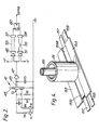
- Figure 2 is a block schematic circuit diagram of a part of the equipment;
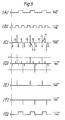
- Figures 3A to 3G illustrate the waveforms of signals appearing at various points of the circuit of Figure 2;
- Figure 4 is a diagrammatic perspective view illustrating one test probe included in the equipment;
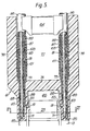
- Figure 5 is a sectional view of a multi-test probe unit included in the equipment;
- Figure 6 is a sectional view along the line VI-VI in Figure 5;
- Figure 7 is a block schematic diagram of an alternative form of the part of the equipment shown in Figure 2; and
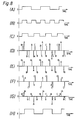
- Figures 8A to 8H illustrate the waveforms of signals appearing at various points of the circuit of Figure 7.
- The equipment is intended for use in the automatic testing of printed circuit boards carrying high speed binary signal circuits of dual-in-line package integrated circuit form.
- Referring to Figure 1, the equipment is intended for use on a table top and is for the most part contained in a
housing 1. - The housing has two
compartments 3 and 5, one housing the power supply units of the equipment and the other housing signal handling circuits of the equipment. - Power supplies for the internal circuits of the equipment are carried on
circuit boards 7 housed in an upper part of the compartment 3 and a power supply 9 and associated switching 11 for anelectric circuit board 13 to be tested, together withother components 15 required to be connected to the board for testing purposes, such as loads, are mounted in removable drawer 17 housed normally in the lower part of the compartment 3, but shown withdrawn in Figure 1. - The
circuit board 13 to be tested is placed in a test jig 19 during testing. Above one half of the circuit board jig 19 there is ajig 21 which carries a number of multi test probe units (not visible in Figure 1, but described below). The probes of the probe units are adapted to be coupled with the pins ofintegrated circuit packages 23 carried on thecircuit board 13 when thecircuit board 13 is slid under theprobe unit jig 21 and theprobe unit jig 21 lowered into position over theboard 13. - In Figure 1, the
circuit board 13 is shown withdrawn from under theprobe unit jig 21 to allow manual application of a single test probe unit 25 (further described below) to a selected point on thecircuit board 13. - The signals picked up by the probe units are fed by way of signal conditioning circuits comprising differentiating and amplifying circuits contained in the
probe unit jig 21 andcomparator units 29 to signal handling circuits carried oncircuit boards 31 housed in an upper part of thecompartment 5 of thehousing 1, thecomparator units 29 being mounted in aremovable drawer 33 housed normally in the lower part of thecompartment 5, but shown withdrawn in Figure 1. - The signal handling circuits carried on the
boards 31 essentially comprise logic circuits for carrying out appropriate tests of the conditioned probe signals supplied via thecomparator units 29. The results of these tests are passed to a computer (not shown) for analysis and display. - Each of the test probes is constructed so as to be capacitively coupled to an integrated circuit package pin or the selected point on the printed circuit board under test so as to load only very lightly the circuit under test. As a consequence of such capacitive coupling there is a high possibility that a probe will pick up an unwanted signal from an adjacent integrated circuit package pin or circuit board conductor. The purpose of the signal conditioning circuits is to suppress such unwanted signals.
- Referring now to Figure 2, each
probe 41 essentially comprises aninner conductor 43 coaxially surrounded, but insulated from, ametal shield 45. Theshield 45 completely encloses theinner conductor 43 except over a small end portion of the inner conductor, which portion is placed adjacent but spaced from the pin or circuit point to be tested in use so as to be capacitively coupled thereto, as represented by capacitor C2 in Figure 2. Each probe is associated with a signal conditioning circuit including anamplifier 47 to whose input a wanted signal is fed via the probe capacitance C2, the wanted signal being represented in Figure 2 by a generator A of internal resistance RA. An unwanted signal fed to the input of theamplifier 47 via the probe capacitance C2 is indicated by a generator B of internal resistance RB. Capacitor C1 represents unavoidable circuit coupling between the pin or circuit point under test and an adjacent pin or circuit point which results in the unwanted signal being fed to theamplifier 47 via theprobe 41. It will be noted that theprobe shield 45 prevents the amplitude of the unwanted signal picked up by theprobe 41 from appreciably exceeding that due to capacitor C1 so that the unwanted signal is of significantly smaller amplitude than the wanted signal. - Capacitor C3 represents the capacitance between the
inner conductor 43 and theshield 45 of theprobe 41, and the resistors R1 and R2 the leakage resistances between the pins or circuit points and ground. - In operation, a wanted binary signal A (Figure 3A), and an unwanted binary signal B (Figure 3B) applied to the probe will be differentiated by the capacitance C2 of the probe and the leakage resistance R2, and a proportion of the differentiated signals (Figure 3C) determined by the relative values of capacitances C2 and C3 applied to the input of
amplifier 47. The output ofamplifier 47 is applied to one input of each of twocomparators comparators 49 and 51 (see Figure 3D), their magnitude lying below the difference between the values of a differentiated A signal and a differentiated B signal at the output of the amplifier, and above the value of a differentiated B signal. - Thus there appears at the outputs of
comparators - It will be understood in this connection that for satisfactory operation the amplitude of the B signals must not appreciably exceed about 40% of the amplitude of the A signals so that if differentiated A and B signals of opposite polarity coincide, as indicated at X in Figure 3C, the resultant signal (Figure 3D) is still significantly greater in amplitude than a B signal.
- The outputs of
comparators transmission lines drivers flop 60, the required inversion of the output ofcomparator 51 being indicated by a cross-over in the conductor oftransmission line 55. - In response to its inputs the flip-
flop 60 thus produces at its output a pulse signal (see Figure 3G) corresponding to the signal A picked up by the probe with the unwanted B signal totally suppressed. - Referring now to Figure 4, the
probe unit 25 suitably comprises a metaltubular body portion 151 to one end of which are secured twometal strips 153, the strips extending at right angles to the axis of the body portion in parallel spaced relationship so that the axis of the gap between the strips intersects the axis of the body portion. Aninsulated conductor 155 extends through thebody portion 151 which at the end of the body portion to which the strips are attached divides into twoparts 155A, 155B the two parts lying in the gap between the strips, one on either side of thebody portion 151. The ends of theconductor 155 andbody portion 151 remote from thestrips 153 are respectively connected to the circuits in theprobe unit jig 21 via the inner and outer of a coaxial cable (not shown). - In use the
end parts 155A and 155B of the inner conductor of the probe must be placed so as to be along the printedcircuit board conductor 157 whose signal is to be monitored, thestrips 153 then serving to shield theend parts 155A, 155B, from acircuit conductor 159 to either side of theconductor 157. - Referring now to Figures 5 and 6, the multi-test probe units attached to the
probe unit jig 21 suitably comprise amoulded body portion 61 of plastics material of generally H-shaped cross- section. - The
lower parts 63 of the vertical limbs of the body portion constitute parallel planar spaced wall portions of thebody 61 which are disposed on either side of acavity 65 which receives a dual-in-line integratedcircuit package 23 in use of the unit. A number ofbores 69 extend vertically through eachwall portion 63, the bores being disposed in parallel spaced relationship in like manner to theconnector pins 71 of thepackage 23. - Each
bore 69 houses ametal tube 73 which at its upper end extends beyond thehorizontal limb 75 of thebody 61 into acavity 77 bounded by theupper parts 79 of the vertical limbs of thebody 61, and at its lower end has an arcuate portion cut away to provide anaperture 81 at its side adjacent thecavity 65, the end of thetube 73 adjacent the arcuate cut-out locating on ashoulder 83 jutting into thebore 69. Apart from theaperture 81 formed by the cut-away portion, eachtube 73 is closed at its lower end, theend closure 85 being embedded in the plastics material of thebody portion 61 during moulding. - In use the unit is lowered onto a
package 23 until the free ends of thewall portions 63 contact thecircuit board 13 carrying thepackage 23. - The inner surfaces of the
wall portions 63 are recessed to receive thepins 71 of thepackage 23 and providelips 89 which fit between thepins 71 and so align theapertures 81 in thetubes 73 with thepins 71. - Along the inside of each
tube 73 there extends theinner conductor 91 and surroundinginsulation 93 of a coaxial screenedcable 95, thescreen 97 of the cable having been stripped back to lie just above the upper end of thetube 73, and the outer insulatingsheath 99 of the cable being stripped back slightly further. The adjacent ends of thecable screen 97, andtube 73 are soldered within ametal sleeve 101 which in turn fits within afurther sleeve 103 of insulating material which extends upwardly beyond the end of themetal sleeve 101 to cover the solder joint between thesleeve 101 and thecable screen 99. - At their upper ends the screened
cables 95 pass out of thebody portion 61 of the unit and thence to the signal conditioning circuits 27 housed in theprobe unit jig 21, the cables being clamped to the body portion by suitably shaped spring loaded clamp means 104 inserted into the upper part of thecavity 77. - As best illustrated in Figure 6, the
aperture 81 in themetal tubes 73 allow the eachinner conductor 91 of each screenedcable 95 to be capacitively coupled to the nearest integratedcircuit package pin 71, thetubes 73 serving to shield theinner conductors 91 from thepins 71 on either side of the nearest pin. Similarly theend closure 85 of eachtube 73 shields the bottom end of the associatedinner conductor 91. - Figure 7 illustrates an alternative form of signal conditioning circuit to that illustrated in Figure 2 which is especially suitable for use in an equipment according to the invention with a probe unit adapted to monitor the signal on a selected one of a line of test points from a position spaced from the selected test point by a sufficiently large amount to render it difficult to avoid excessive pick-up from adjacent test points by the use of screening. Such a situation may arise for example when testing signals on a so-called conformally coated printed circuit card, i.e. a printed circuit board of which the conductors and components are protected by an insulating coating, or when using the probe, unit to scan along a line of test points to find a particular signal.
- Referring to Figure 7, the
probe unit 105 comprises three probes formed by threeconductors metal shield 113. The shield completely encloses each conductor except over a small end portion. In use the exposed end portion of thecentral conductor 109 is placed adjacent but spaced from acircuit lead 115 carrying a signal A to be tested so as to be capacitively coupled thereto. Theconductors 107 to 111 are spaced so that the exposed end portions of the other twoconductors 107 and 111 will then be adjacent circuit leads 117 and 119 on either side of thelead 115, the leads carrying signals B and C respectively. - The signal conditioning circuit comprises a
differential amplifier 121 having one input directly connected to theconductor 109 and via aresistor 123 to ground. The other input of theamplifier 121 is connected to ground via apotentiometer 125 whose variable capping point is connected to each of theconductors 107 and 111. The leads between theamplifier 121 and theprobe unit 105 are individually screened as indicated bydotted line 127. - The output of the
amplifier 121 is applied to a comparator and flip-flop arrangement 49 to 61 of the same form as shown in Figure 2. - In operation binary signals A, B and C appearing on circuit leads 115, 117 and 119 (Figures 8A, 8B and 8C) will all be picked up by the
central conductor 109 and differentiated as described above with reference to Figure 2 giving rise to a signal at one input of theamplifier 121 as shown in Figure 8D, the differentiated A signals fromlead 115 being larger than those from the other twoleads - The other two
conductors 107 and 111 respectively give rise to differentiated A and B signals fromleads leads amplifier 121, as shown in Figures 8E and 8F respectively. In theamplifier 121 the differentiated B and C signals tend to cancel giving rise to a signal at the output ofamplifier 121 as shown in Figure 8G wherein the differentiated A signals are appreciably larger compared with the B and C signals than in the signal at the input of theamplifier 121 connected toconductor 109. - The comparator and flip-
flop arrangement 49 to 61 then produces at its output a pulse signal (Fig. 8H) corresponding to signal A with the unwanted signals B and C totally suppressed, as described above with reference to Figures 2 and 3. - It will be appreciated that the
potentiometer 125 is used to balance the B and C signals picked up byconductor 109 against the B and C signals picked up byconductors 107 and 111. - It will be understood that a signal conditioning circuit as shown in Figure 7 is especially adapted for use with a multi-test probe unit as shown in Figures 5 and 6, the conditioning circuit being arranged to utilise as inputs the signal produced by any selected adjacent three probes of the unit by means of a suitable selector circuit arrangement.
- It will further be understood that a signal conditioning circuit of the form shown in Figure 7 may also be modified so as to utilise the signals produced by two or more than three adjacent probes, where the disposition of test points in a circuit to be tested require this.
Claims (9)
Applications Claiming Priority (2)
| Application Number | Priority Date | Filing Date | Title |
|---|---|---|---|
| GB848423310A GB8423310D0 (en) | 1984-09-14 | 1984-09-14 | Electric circuit testing equipment |
| GB8423310 | 1984-09-14 |
Publications (2)
| Publication Number | Publication Date |
|---|---|
| EP0177210A1 EP0177210A1 (en) | 1986-04-09 |
| EP0177210B1 true EP0177210B1 (en) | 1990-05-23 |
Family
ID=10566737
Family Applications (1)
| Application Number | Title | Priority Date | Filing Date |
|---|---|---|---|
| EP85306525A Expired EP0177210B1 (en) | 1984-09-14 | 1985-09-13 | Electric circuit testing equipment |
Country Status (5)
| Country | Link |
|---|---|
| US (1) | US4801866A (en) |
| EP (1) | EP0177210B1 (en) |
| JP (1) | JPS61105475A (en) |
| DE (1) | DE3577921D1 (en) |
| GB (2) | GB8423310D0 (en) |
Families Citing this family (32)
| Publication number | Priority date | Publication date | Assignee | Title |
|---|---|---|---|---|
| FR2651580B1 (en) * | 1989-09-05 | 1991-12-13 | Aerospatiale | DEVICE FOR THE DIELECTRIC CHARACTERIZATION OF SAMPLES OF PLANE OR NON-PLANAR SURFACE MATERIAL AND APPLICATION TO NON-DESTRUCTIVE INSPECTION OF THE DIELECTRIC HOMOGENEITY OF SAID SAMPLES. |
| EP0432904A3 (en) * | 1989-11-15 | 1991-09-11 | Raychem Corporation (A Delaware Corporation) | Cable television connection system |
| US5625292A (en) * | 1990-12-20 | 1997-04-29 | Hewlett-Packard Company | System for measuring the integrity of an electrical contact |
| US5557209A (en) * | 1990-12-20 | 1996-09-17 | Hewlett-Packard Company | Identification of pin-open faults by capacitive coupling through the integrated circuit package |
| US5274336A (en) * | 1992-01-14 | 1993-12-28 | Hewlett-Packard Company | Capacitively-coupled test probe |
| US5696451A (en) * | 1992-03-10 | 1997-12-09 | Hewlett-Packard Co. | Identification of pin-open faults by capacitive coupling |
| GB9212646D0 (en) * | 1992-06-15 | 1992-07-29 | Marconi Instruments Ltd | A method of and equipment for testing the electrical conductivity of a connection |
| FR2697636B1 (en) * | 1992-11-03 | 1994-11-25 | Thomson Csf | Device for broadband microwave tests performed in situ. |
| US5420500A (en) * | 1992-11-25 | 1995-05-30 | Hewlett-Packard Company | Pacitive electrode system for detecting open solder joints in printed circuit assemblies |
| US5426372A (en) * | 1993-07-30 | 1995-06-20 | Genrad, Inc. | Probe for capacitive open-circuit tests |
| US5945634A (en) * | 1995-04-24 | 1999-08-31 | Raychem Corporation | Coaxial cable tap with slitted housing and non-piercing tap insert |
| JP2994259B2 (en) | 1996-03-28 | 1999-12-27 | オー・エイチ・ティー株式会社 | Substrate inspection method and substrate inspection device |
| US5867020A (en) * | 1996-10-31 | 1999-02-02 | Sematech, Inc. | Capacitively coupled RF voltage probe having optimized flux linkage |
| US6014032A (en) * | 1997-09-30 | 2000-01-11 | International Business Machines Corporation | Micro probe ring assembly and method of fabrication |
| US6059982A (en) * | 1997-09-30 | 2000-05-09 | International Business Machines Corporation | Micro probe assembly and method of fabrication |
| US6411108B1 (en) | 1999-11-05 | 2002-06-25 | Sensor Technologies, Inc. | Noncontact signal analyzer |
| US7088175B2 (en) * | 2001-02-13 | 2006-08-08 | Quantum Applied Science & Research, Inc. | Low noise, electric field sensor |
| US6545483B1 (en) | 2001-08-29 | 2003-04-08 | Sensor Technologies, Inc. | Analyzer sensor |
| US8923956B2 (en) | 2001-12-07 | 2014-12-30 | The University Of Sussex | Electrodynamic sensors and applications thereof |
| GB0129390D0 (en) * | 2001-12-07 | 2002-01-30 | Clark Terrence D | Electrodynamic sensors and applications thereof |
| US6828767B2 (en) | 2002-03-20 | 2004-12-07 | Santronics, Inc. | Hand-held voltage detection probe |
| US6961601B2 (en) * | 2003-06-11 | 2005-11-01 | Quantum Applied Science & Research, Inc. | Sensor system for measuring biopotentials |
| WO2005036096A2 (en) * | 2003-10-07 | 2005-04-21 | Quantum Applied Science And Research, Inc. | Measuring vector components of an electric field |
| US7173437B2 (en) * | 2004-06-10 | 2007-02-06 | Quantum Applied Science And Research, Inc. | Garment incorporating embedded physiological sensors |
| CA2477615A1 (en) * | 2004-07-15 | 2006-01-15 | Quantum Applied Science And Research, Inc. | Unobtrusive measurement system for bioelectric signals |
| US20060041196A1 (en) * | 2004-08-17 | 2006-02-23 | Quasar, Inc. | Unobtrusive measurement system for bioelectric signals |
| US20060192545A1 (en) * | 2005-02-28 | 2006-08-31 | Static Control Components, Inc. | Voltage detection pole |
| US7622931B2 (en) * | 2005-10-03 | 2009-11-24 | University Of Utah Research Foundation | Non-contact reflectometry system and method |
| US20090201038A1 (en) * | 2008-02-11 | 2009-08-13 | Knickerbocker John U | Test head for functional wafer level testing, system and method therefor |
| US8760185B2 (en) * | 2009-12-22 | 2014-06-24 | Anthony J. Suto | Low capacitance probe for testing circuit assembly |
| US8310256B2 (en) * | 2009-12-22 | 2012-11-13 | Teradyne, Inc. | Capacitive opens testing in low signal environments |
| US10034300B2 (en) * | 2010-06-10 | 2018-07-24 | Cisco Technology, Inc | Load based probe response scheduling |
Family Cites Families (18)
| Publication number | Priority date | Publication date | Assignee | Title |
|---|---|---|---|---|
| US2750562A (en) * | 1952-09-16 | 1956-06-12 | Gen Electric | Insulation fault detector |
| US3388423A (en) * | 1964-08-28 | 1968-06-18 | Bell Telephone Labor Inc | Methods and apparatus for measuring characteristics of an insulating sheet in an electroconductive fluid |
| US3918306A (en) * | 1974-03-15 | 1975-11-11 | Drexelbrook Controls | System for measuring fluid levels in a vehicle transmission |
| DE2502715C3 (en) * | 1975-01-23 | 1978-03-23 | Siemens Ag, 1000 Berlin Und 8000 Muenchen | Capacitive pickup for ignition systems of internal combustion engines |
| US4083038A (en) * | 1975-06-09 | 1978-04-04 | Elkay Electronics Ltd. | Condenser plate assembly |
| US3943367A (en) * | 1975-06-10 | 1976-03-09 | The United States Of America As Represented By The Secretary Of The Army | High frequency optically coupled differential voltage probe with logarithmic response |
| US4012097A (en) * | 1975-10-17 | 1977-03-15 | Everett/Charles, Inc. | Combined test clip and component extraction tool |
| US4115731A (en) * | 1976-06-01 | 1978-09-19 | Digital Facilities, Inc. | System for locating electrical shorts by tracking the paths of injected pulse currents utilizing a voltage differential responsive probe |
| US4054835A (en) * | 1976-11-22 | 1977-10-18 | General Electric Company | Rapid response generating voltmeter |
| US4085361A (en) * | 1977-03-10 | 1978-04-18 | Wiltron Company | Measurement of frequency response with improved sensitivity and accuracy |
| US4245352A (en) * | 1979-03-07 | 1981-01-13 | International Jensen Incorporated | Automated system for testing radio receivers |
| US4345201A (en) * | 1979-12-20 | 1982-08-17 | Membrain Limited | Fault location system with enhanced noise immunity |
| US4574235A (en) * | 1981-06-05 | 1986-03-04 | Micro Component Technology, Inc. | Transmission line connector and contact set assembly for test site |
| US4419626A (en) * | 1981-08-25 | 1983-12-06 | Daymarc Corporation | Broad band contactor assembly for testing integrated circuit devices |
| US4532442A (en) * | 1981-10-23 | 1985-07-30 | Black Ian A | Noise reduction in electronic measuring circuits |
| JPS5873881A (en) * | 1981-10-29 | 1983-05-04 | Advantest Corp | Ic tester |
| DD208676A1 (en) * | 1982-07-22 | 1984-04-04 | Robotron Rationalisierung | DEVICE FOR A CONTACT PIN FOR THE CONTACTLESS TRACKING OF POWER SUPPLIES, PREFERABLY DIGITAL CIRCUITS |
| GB2143954A (en) * | 1983-07-22 | 1985-02-20 | Sharetree Ltd | A capacitive method and apparatus for checking connections of a printed circuit board |
-
1984
- 1984-09-14 GB GB848423310A patent/GB8423310D0/en active Pending
-
1985
- 1985-09-11 US US06/774,795 patent/US4801866A/en not_active Expired - Fee Related
- 1985-09-13 JP JP60201899A patent/JPS61105475A/en active Pending
- 1985-09-13 DE DE8585306525T patent/DE3577921D1/en not_active Expired - Fee Related
- 1985-09-13 EP EP85306525A patent/EP0177210B1/en not_active Expired
- 1985-09-13 GB GB08522676A patent/GB2164456B/en not_active Expired
Also Published As
| Publication number | Publication date |
|---|---|
| GB2164456A (en) | 1986-03-19 |
| EP0177210A1 (en) | 1986-04-09 |
| GB8423310D0 (en) | 1984-10-17 |
| US4801866A (en) | 1989-01-31 |
| JPS61105475A (en) | 1986-05-23 |
| GB2164456B (en) | 1988-08-24 |
| DE3577921D1 (en) | 1990-06-28 |
| GB8522676D0 (en) | 1985-10-16 |
Similar Documents
| Publication | Publication Date | Title |
|---|---|---|
| US4801866A (en) | Electric circuit testing equipment | |
| US5274336A (en) | Capacitively-coupled test probe | |
| EP0862062B1 (en) | Circuit board inspection apparatus and method | |
| US5420500A (en) | Pacitive electrode system for detecting open solder joints in printed circuit assemblies | |
| US8461855B2 (en) | Device interface board with cavity back for very high frequency applications | |
| JPS6195259A (en) | Improved wide-band contactor assembly for testing integratedcircuit device | |
| US7332923B2 (en) | Test probe for high-frequency measurement | |
| DE112009005186B4 (en) | SIGNAL DETECTION DEVICES AND CIRCUIT BOARD | |
| US5218293A (en) | Passive high-frequency signal probe | |
| US5446393A (en) | Electrical measuring and testing probe having a malleable shaft facilitating positioning of a contact pin | |
| JPH08248080A (en) | Electromagnetic noise measuring magnetic field probe, electromagnetic noise measuring electric field probe and electromagnetic noise measuring apparatus | |
| CN209215446U (en) | It is a kind of for testing the probe and noise-measuring system of common-mode noise | |
| US5808475A (en) | Semiconductor probe card for low current measurements | |
| US20020151193A1 (en) | Solder-down printed circuit board connection structure | |
| US3743925A (en) | Adapter for terminating multiconductor signal transmission cable | |
| JPH10142291A (en) | Ic tester | |
| US20080186036A1 (en) | High Speed Electrical Probe | |
| US4099119A (en) | Probe apparatus for in place testing of electrical circuit boards | |
| US20030071643A1 (en) | High-density PCB test jack | |
| US6498299B2 (en) | Connection structure of coaxial cable to electric circuit substrate | |
| US20030152153A1 (en) | Signaling through electromagnetic couplers | |
| CN215379335U (en) | A kind of PCB impedance test structure and PCB board | |
| KR19990017233A (en) | High Frequency Probe Card | |
| JP2007278781A (en) | Semiconductor evaluation equipment | |
| US7091732B2 (en) | Systems and methods for probing processor signals |
Legal Events
| Date | Code | Title | Description |
|---|---|---|---|
| PUAI | Public reference made under article 153(3) epc to a published international application that has entered the european phase |
Free format text: ORIGINAL CODE: 0009012 |
|
| AK | Designated contracting states |
Kind code of ref document: A1 Designated state(s): DE FR GB IT |
|
| 17P | Request for examination filed |
Effective date: 19861006 |
|
| 17Q | First examination report despatched |
Effective date: 19880810 |
|
| RAP1 | Party data changed (applicant data changed or rights of an application transferred) |
Owner name: GEC-MARCONI LIMITED |
|
| RBV | Designated contracting states (corrected) |
Designated state(s): DE FR IT |
|
| GRAA | (expected) grant |
Free format text: ORIGINAL CODE: 0009210 |
|
| AK | Designated contracting states |
Kind code of ref document: B1 Designated state(s): DE FR IT |
|
| ITF | It: translation for a ep patent filed | ||
| ET | Fr: translation filed | ||
| REF | Corresponds to: |
Ref document number: 3577921 Country of ref document: DE Date of ref document: 19900628 |
|
| PGFP | Annual fee paid to national office [announced via postgrant information from national office to epo] |
Ref country code: FR Payment date: 19900810 Year of fee payment: 6 |
|
| ITTA | It: last paid annual fee | ||
| PGFP | Annual fee paid to national office [announced via postgrant information from national office to epo] |
Ref country code: DE Payment date: 19901127 Year of fee payment: 6 |
|
| PLBE | No opposition filed within time limit |
Free format text: ORIGINAL CODE: 0009261 |
|
| STAA | Information on the status of an ep patent application or granted ep patent |
Free format text: STATUS: NO OPPOSITION FILED WITHIN TIME LIMIT |
|
| 26N | No opposition filed | ||
| PG25 | Lapsed in a contracting state [announced via postgrant information from national office to epo] |
Ref country code: FR Effective date: 19920529 |
|
| PG25 | Lapsed in a contracting state [announced via postgrant information from national office to epo] |
Ref country code: DE Effective date: 19920602 |
|
| REG | Reference to a national code |
Ref country code: FR Ref legal event code: ST |