EP0176028A2 - Method for producing a laser diode with a buried active layer and with lateral current confinement by a self-adjusted p-n junction - Google Patents
Method for producing a laser diode with a buried active layer and with lateral current confinement by a self-adjusted p-n junction Download PDFInfo
- Publication number
- EP0176028A2 EP0176028A2 EP85111813A EP85111813A EP0176028A2 EP 0176028 A2 EP0176028 A2 EP 0176028A2 EP 85111813 A EP85111813 A EP 85111813A EP 85111813 A EP85111813 A EP 85111813A EP 0176028 A2 EP0176028 A2 EP 0176028A2
- Authority
- EP
- European Patent Office
- Prior art keywords
- layer
- doping
- dopant
- redoping
- laser
- Prior art date
- Legal status (The legal status is an assumption and is not a legal conclusion. Google has not performed a legal analysis and makes no representation as to the accuracy of the status listed.)
- Granted
Links
Images
Classifications
-
- H—ELECTRICITY
- H01—ELECTRIC ELEMENTS
- H01S—DEVICES USING THE PROCESS OF LIGHT AMPLIFICATION BY STIMULATED EMISSION OF RADIATION [LASER] TO AMPLIFY OR GENERATE LIGHT; DEVICES USING STIMULATED EMISSION OF ELECTROMAGNETIC RADIATION IN WAVE RANGES OTHER THAN OPTICAL
- H01S5/00—Semiconductor lasers
- H01S5/20—Structure or shape of the semiconductor body to guide the optical wave ; Confining structures perpendicular to the optical axis, e.g. index or gain guiding, stripe geometry, broad area lasers, gain tailoring, transverse or lateral reflectors, special cladding structures, MQW barrier reflection layers
- H01S5/22—Structure or shape of the semiconductor body to guide the optical wave ; Confining structures perpendicular to the optical axis, e.g. index or gain guiding, stripe geometry, broad area lasers, gain tailoring, transverse or lateral reflectors, special cladding structures, MQW barrier reflection layers having a ridge or stripe structure
- H01S5/227—Buried mesa structure ; Striped active layer
-
- H—ELECTRICITY
- H01—ELECTRIC ELEMENTS
- H01S—DEVICES USING THE PROCESS OF LIGHT AMPLIFICATION BY STIMULATED EMISSION OF RADIATION [LASER] TO AMPLIFY OR GENERATE LIGHT; DEVICES USING STIMULATED EMISSION OF ELECTROMAGNETIC RADIATION IN WAVE RANGES OTHER THAN OPTICAL
- H01S5/00—Semiconductor lasers
- H01S5/20—Structure or shape of the semiconductor body to guide the optical wave ; Confining structures perpendicular to the optical axis, e.g. index or gain guiding, stripe geometry, broad area lasers, gain tailoring, transverse or lateral reflectors, special cladding structures, MQW barrier reflection layers
- H01S5/2054—Methods of obtaining the confinement
- H01S5/2059—Methods of obtaining the confinement by means of particular conductivity zones, e.g. obtained by particle bombardment or diffusion
-
- H—ELECTRICITY
- H01—ELECTRIC ELEMENTS
- H01S—DEVICES USING THE PROCESS OF LIGHT AMPLIFICATION BY STIMULATED EMISSION OF RADIATION [LASER] TO AMPLIFY OR GENERATE LIGHT; DEVICES USING STIMULATED EMISSION OF ELECTROMAGNETIC RADIATION IN WAVE RANGES OTHER THAN OPTICAL
- H01S5/00—Semiconductor lasers
- H01S5/20—Structure or shape of the semiconductor body to guide the optical wave ; Confining structures perpendicular to the optical axis, e.g. index or gain guiding, stripe geometry, broad area lasers, gain tailoring, transverse or lateral reflectors, special cladding structures, MQW barrier reflection layers
- H01S5/22—Structure or shape of the semiconductor body to guide the optical wave ; Confining structures perpendicular to the optical axis, e.g. index or gain guiding, stripe geometry, broad area lasers, gain tailoring, transverse or lateral reflectors, special cladding structures, MQW barrier reflection layers having a ridge or stripe structure
- H01S5/227—Buried mesa structure ; Striped active layer
- H01S5/2275—Buried mesa structure ; Striped active layer mesa created by etching
Definitions
- the present invention relates to a laser diode as specified in the preamble of claim 1.
- Buried hetero-laser buried active layer type diodes including the laser diode of the present invention, are known from, for example, US Pat. No. 4,426,700 and IEEE Journ. of Quantum Electronics, Vol. QE-15 (1979), pp. 451 to 469, this document discussing the theoretical questions more. These are laser diodes in a semiconductor body with a hetero-layer structure. To achieve the lowest threshold currents, the spatial arrangement is such that the active layer, which has the shape of a narrow strip, also referred to as a web, is located within the layer structure, ie is buried, this narrow strip of semiconductor material having a lower refractive index and flanked by a higher band gap.
- the arrangement is made in such a way and the laser diode is constructed in such a way that the electrical current which is used to generate the laser radiation is concentrated on this narrow strip and that leakage currents which occur in the vicinity of the active strip are suppressed.
- insulating layers have been used to suppress such leakage currents.
- pn junctions it is also known to use pn junctions for this purpose, but there is always the problem that this leads to the through strip being active flowing electrical current is adversely affected. By locally selective growth of pn junction layers next to the active strip, the occurrence of such an influence can be avoided, but this is a very complex manufacturing process.
- the object of the present invention is to provide such a laser diode of the buried strip-shaped active layer type, in which the laterally arranged pn junction, which serves to restrict the current to the active strip, can be attached in a simple manner and yet does not influence the generation of the laser radiation serving current flowing through the active strip.
- a known method for producing a laser diode with a buried active layer, including lateral regions with a lower refractive index and a higher band gap, has been carried out in accordance with US Pat. No. 4,426,700 in such a way that the hetero-layer structure of the diode is initially applied over the entire surface of a substrate body has been produced and then the web containing the narrow strip of the active layer has been produced by masked etching, ie by etching away the lateral zones. Only then do these zones on the side of the web be refilled with epitaxially deposited semiconductor material. These measures are cumbersome and it is also difficult to ensure the exact position of a pn junction which is to be produced in connection with this refilling and which extends to the side of the web.
- One idea on which the invention is based is to dimension or design individual process parameters of the production process of a diode according to the invention in such a way that the desired pn transition results in principle in the course of the production process.
- the invention provides that this pn junction is self-adjusting.
- a layer is provided which contains a heavily diffusing dopant of this type, which diffuses into another of the layers of the layer structure in the course of a heat treatment process or annealing process and causes redoping there.
- This other layer is such a layer which is separated from the first-mentioned layer originally (alone) containing the dopant by an intermediate layer of the entire layer structure.
- the invention also includes the selection and the dimensioning that this further layer is doped with respect to the first-mentioned layer in such a way that it is doped in opposite directions with respect to this first-mentioned layer.
- the extent of this doping of this further layer is chosen so that the conduction type of this further adjacent layer is not changed when the dopant diffuses out of the former layer during the heat treatment.
- the dimensions are also selected so that the proportion of the dopant diffusing through this further layer into the other layer causes such a redoping in this other layer, at least in the border area between this other layer and the further layer, that a The transition between this redoped portion of the other layer and the further layer, which has remained unchanged in terms of its doping type, has arisen.
- the dimensions, in particular those of the degrees of doping are such that there is no redoping for the layers of the buried laser zone belonging to the laser-active strip.
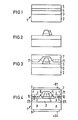
- a hetero-layer structure is shown, as it is usually used in principle for lasers with buried active layer.
- 2 denotes a semiconductor substrate, which e.g. consists of p-conducting indium phosphide.
- the first layer 3 located thereon consists, for example, of p-type indium phosphide which is doped according to the invention with a dopant which has a high diffusion coefficient, i.e. shows strongly diffusing tendency. In particular, such a dopant is zinc. However, cadmium and / or magnesium can also be used.
- the second layer 4 consists e.g. from indium gallium arsenide phosphide. It is the actual active layer and is preferably undoped.
- Layer 5 consists e.g. made of n-conducting indium phosphide.
- a dopant is used which (compared to that of layer 3) has a less high, in particular very small, diffusion coefficient.
- This type of layer structure known in the art, thus contains a pn junction, which is polarized in the direction of flow during operation of the laser diode.
- Fig. 2 shows the result of an etching process by means of which the usual strip-like structure of layers 4 and 5, i.e. the laser-active zone of the layer 4 and the subsequent contact layer 5.
- Layer 6 which has been referred to above as a further layer, consists, for example, of n-conducting indium phosphide. It is preferably doped with only weakly diffusing dopant, e.g. with tin, tellurium or germanium.
- the degree of doping of the further layer 6 is so much higher than that of the other layer 7 that during the heat treatment from the first-mentioned layer 3 into layers 6 and 7 diffusing dopant, e.g. the zinc contained in layer 3, in the further layer 6 does not yet cause a redoping, but in layer 7 the zone of layer 7 denoted by 71 is redoped.
- This zone 71 extends to the right and left of the strip-shaped active layer 4. Seen from zone 71, which has become p-type due to the (additional) zinc doping, layer 6, which has remained n-type, and then p conductive layer 3. There is thus a pnp transition from zone 71 to layer 3, which contains a pn transition blocking the current next to the laser strip. This blocking pn junction has arisen due to the entire manufacturing process of the laser diode according to the invention.
- the heat treatment process can be carried out separately. However, the heat treatment may already be part of the epitaxial process of layers 6 and 7, i.e. the diffusion of the zinc can take place in the course of the formation of the layers 6 and 7.
- FIG. 4 shows a finished laser diode manufactured according to the method steps of FIGS. 1 to 3. It is also provided with electrodes 8 and 9, which are used to connect the electrical supply voltage. From the dopings given in this figure, which are to be understood as an example, it can be seen that, in the region of the laser-active strip, the pn junction which is poled in the direction of flow is desirably present unchanged. To the right and left of this strip-shaped zone 4 are the ones produced according to the invention blocking pn junctions 10 (highlighted with crosses in the figure), which have the effect that the current flow is restricted to the strip-shaped laser-active zone.
- the manufacturing method according to the invention can also be seen on the finished laser diode according to FIG. the invention very characteristic distributions of the doping and the relative dimensions of the doping to each other.
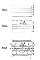
- the semiconductor substrate is designated by 12, but here it is n-conducting, for example again indium phosphide.
- the subsequent first layer 13 is also n-conducting, for example tin-doped indium phosphide.
- the next layer 14 is n-conducting and, for example, again tin-doped indium phosphide, but with a higher degree of doping than layer 13.
- the next layer 15 is the actual active layer (to be compared with layer 4) made of, for example, indium gallium arsenide phosphide, which e.g. is undoped.
- the next layer 16 is p-type, e.g. zinc doped indium phosphide.
- FIG. 6 shows the result of the method step of the etching with the strip-shaped structure of the active zone 15 and 16 that can be seen in the figure.
- next layer 17 which is the layer which contains the dopant with a large diffusion coefficient provided according to the invention.
- the p-type dopant in particular zinc, cadmium or magnesium.
- the degree of doping of the n-type ones Layer 14 is chosen to be so much larger than that of n-type layer 13 that p-type dopant diffusing in and through layer 17 (with appropriate heat treatment) from layer 17 does not change the conductivity type of this layer 14, but does change that of the layer 13 changed.
- the laser diode according to FIG. 8 shows the result of the manufacturing method according to the invention, namely the laser diode of the second exemplary embodiment provided with the electrodes 8 and 9.
- the laser diode according to FIG. 8 also has a pnp structure with a blocking pn junction 10 outside the actual laser-active zone of strips 3 and 4.
- dimensions relating to the invention are given for the two exemplary embodiments.
Abstract
Laserdiode mit vergrabener aktiver Schicht und mit seitlicher Strombegrenzung durch selbstjustierten pn-Übergang sowie Verfahren zur Herstellung einer solchen Laserdiode. Laserdiode (1) mit den streifenförmigen Laser-Übergang (4, 5) seitlich flankierenden Bereichen, in denen ein den Laserstrom sperrender pn-Übergang (10) dadurch erzeugt ist, daß durch Dotierstoffdiffusion (171) aus einer Schicht (3) über eine angrenzende weitere Schicht (6) hinweg in einer an diese Schicht (6) angrenzenden, anderen Schicht (7) Umdotierung (71) erzeugt worden ist.Laser diode with buried active layer and with lateral current limitation through self-adjusted pn junction and method for producing such a laser diode. Laser diode (1) with the strip-shaped laser junction (4, 5) laterally flanking areas, in which a pn junction (10) which blocks the laser current is produced by dopant diffusion (171) from one layer (3) over an adjacent one a further layer (6) has been generated in another layer (7) redoping (71) adjacent to this layer (6).
Description
Die vorliegende Erfindung bezieht sich auf eine Laserdiode, wie im Oberbegriff des Patentanspruchs 1 angegeben.The present invention relates to a laser diode as specified in the preamble of claim 1.
Laserdioden des Typs mit vergrabener aktiver Schicht (Buried Hetero-Laser), zu dem auch die Laserdiode der vorliegenden Erfindung gehört, sind bekannt aus z.B. der US-PS 4 426 700 und aus IEEE Journ. of Quantum Electronics, Bd. QE-15 (1979), S. 451 bis 469, wobei diese Druckschrift mehr die theoretischen Fragen erörtert. Es handelt sich hier um Laserdioden in einem Halbleiterkörper mit Hetero-Schichtaufbau. Zur Erzielung geringster Schwellenströme ist die räumliche Anordnung derart getroffen, daß sich die aktive Schicht, die die Form eines schmalen Streifens, auch als Steg bezeichnet, hat, innerhalb des Schichtaufbaues befindet, d.h. vergraben ist, wobei dieser schmale Streifen von Halbleitermaterial mit niedrigerem Brechungsindex und höherem Bandabstand flankiert ist. Die Anordnung ist so getroffen und die Laserdiode ist so aufgebaut, daß der zugeführte, zur Erzeugung der Laserstrahlung dienende elektrische Strom auf diesen schmalen Streifen konzentriert ist, und daß durch Nebenschlüsse in der Nachbarschaft des aktiven Streifens auftretende Leckströme unterdrückt sind. Für die Unterdrückung solcher Leckströme sind zum einen Isolierschichten verwendet worden. Es ist auch bekannt, hierfür sperrende pn-Übergänge zu verwenden, wobei stets das Problem besteht, daß dadurch der durch den aktiven Streifen fließende elektrische Strom unerwünschterweise beeinträchtigt wird. Durch örtlich selektives Aufwachsen von pn-Übergangsschichten neben dem aktiven Streifen läßt sich zwar das Auftreten einer solchen Beeinflussung vermeiden, doch ist dies ein sehr aufwendiges Herstellungsverfahren.Buried hetero-laser buried active layer type diodes, including the laser diode of the present invention, are known from, for example, US Pat. No. 4,426,700 and IEEE Journ. of Quantum Electronics, Vol. QE-15 (1979), pp. 451 to 469, this document discussing the theoretical questions more. These are laser diodes in a semiconductor body with a hetero-layer structure. To achieve the lowest threshold currents, the spatial arrangement is such that the active layer, which has the shape of a narrow strip, also referred to as a web, is located within the layer structure, ie is buried, this narrow strip of semiconductor material having a lower refractive index and flanked by a higher band gap. The arrangement is made in such a way and the laser diode is constructed in such a way that the electrical current which is used to generate the laser radiation is concentrated on this narrow strip and that leakage currents which occur in the vicinity of the active strip are suppressed. On the one hand, insulating layers have been used to suppress such leakage currents. It is also known to use pn junctions for this purpose, but there is always the problem that this leads to the through strip being active flowing electrical current is adversely affected. By locally selective growth of pn junction layers next to the active strip, the occurrence of such an influence can be avoided, but this is a very complex manufacturing process.
Lediglich der Vollständigkeit halber sei auf einen die seitlichen Zonen mit niedrigerem Brechungsindex und höherem Bandabstand nicht umfassenden anderen Typ (gain-guided) einer Laserdiode hingewiesen, der z.B. in der DE-OS 28 19 843 und in Appl. Phys. Lett., Bd. 43 (1983) S. 809 bis 811 sowie Bd. 44 (1984) S. 1035 bis 1037 beschrieben ist.Merely for the sake of completeness, reference should be made to a different type (gain-guided) of a laser diode which does not encompass the lateral zones with a lower refractive index and a higher band gap, which e.g. in DE-OS 28 19 843 and in Appl. Phys. Lett., Vol. 43 (1983) pp. 809 to 811 and Vol. 44 (1984) pp. 1035 to 1037.
Aufgabe der vorliegenden Erfindung ist es, eine solche Laserdiode des Typs vergrabener streifenförmiger aktiver Schicht anzugeben, bei der der seitlich angeordnete pn- Übergang, der der Eingrenzung des Stromes auf den aktiven Streifen dient, in einfacher Weise anzubringen ist und dennoch keine Beeinflussung des der LaserstrahlungsErzeugung dienenden, durch den aktiven Streifen fließenden Stromes bewirkt.The object of the present invention is to provide such a laser diode of the buried strip-shaped active layer type, in which the laterally arranged pn junction, which serves to restrict the current to the active strip, can be attached in a simple manner and yet does not influence the generation of the laser radiation serving current flowing through the active strip.
Diese Aufgabe ist mit einer Laserdiode gelöst, die die Merkmale des Kennzeichens des Patentanspruchs 1 aufweist. Weitere Ausgestaltungen und Weiterbildungen sowie ein Herstellungsverfahren dieser Diode gehen aus den Unteransprüchen hervor.This object is achieved with a laser diode which has the features of the characterizing part of patent claim 1. Further refinements and developments as well as a manufacturing method of this diode emerge from the subclaims.
Ein bekanntes Verfahren zur Herstellung einer Laserdiode mit vergrabener aktiver Schicht, eingeschlossen seitliche Bereiche mit niedrigerem Brechungsindex und höherem Bandabstand, ist entsprechend der US-PS 4 426 700 in der Weise durchgeführt worden, daß auf einem Substratkörper zunächst ganzflächig die Hetero-Schichtstruktur der Diode erzeugt worden ist und dann der den schmalen Streifen der aktiven Schicht enthaltende Steg durch maskiertes Ätzen, d.h. durch Wegätzen der seitlichen Zonen, hergestellt worden ist. Erst nachfolgend werden dann diese Zonen seitlich des Steges wieder mit epitaktisch abgeschiedenem Halbleitermaterial neu aufgefüllt. Diese Maßnahmen sind umständlich und es ist auch schwierig, die genaue Lage eines pn-Überganges zu gewährleisten, der im Zusammenhang mit diesem Wiederauffüllen und sich seitlich des Steges erstreckend zu erzeugen ist.A known method for producing a laser diode with a buried active layer, including lateral regions with a lower refractive index and a higher band gap, has been carried out in accordance with US Pat. No. 4,426,700 in such a way that the hetero-layer structure of the diode is initially applied over the entire surface of a substrate body has been produced and then the web containing the narrow strip of the active layer has been produced by masked etching, ie by etching away the lateral zones. Only then do these zones on the side of the web be refilled with epitaxially deposited semiconductor material. These measures are cumbersome and it is also difficult to ensure the exact position of a pn junction which is to be produced in connection with this refilling and which extends to the side of the web.
Ein der Erfindung zugrundeliegender Gedanke ist, einzelne Verfahrensparameter des Herstellungsverfahrens einer erfindungsgemäßen Diode so zu bemessen bzw. auszugestalten, daß sich der gewünschte pn-Übergang prinzipiell im Verlauf des Herstellungsverfahrens ergibt. Insbesondere ist bei der Erfindung vorgesehen, daß dieser pn-Übergang selbstjustierend entsteht. Bei der erfindungsgemäßen Laserdiode ist eine Schicht vorgesehen, die einen stark diffundierenden, derartigen Dotierungsstoff enthält, der im Verlauf eines Wärmebehandlungsprozesses bzw. Temperprozesses in eine andere der Schichten des Schichtaufbaues eindiffundiert und dort Umdotierung bewirkt. Dabei ist diese andere Schicht eine solche Schicht, die von der den Dotierungsstoff ursprünglich (allein) enthaltenden, erstgenannten Schicht durch eine dazwischenliegende weitere Schicht des gesamten Schichtaufbaues getrennt ist. Zur Erfindung gehört aber weiterhin die Auswahl und die Bemessung, daß diese weitere Schicht gegenüber der erstgenannten Schicht so dotiert ist, daß sie gegenüber dieser erstgenannten Schicht entgegengesetzt dotiert ist. Das Maß dieser Dotierung dieser weiteren Schicht ist so gewählt, daß bei der während der Wärmebehandlung erfolgenden Ausdiffusion des Dotierstoffes aus der erstgenannten Schicht der Leitungstyp dieser weiteren angrenzenden Schicht nicht umgeändert wird. Die Bemessungen sind des weiteren aber auch so gewählt, daß der durch diese weitere Schicht hindurch bis in die andere Schicht diffundierende Anteil des Dotierstoffes dort in dieser anderen Schicht wenigstens im Grenzbereich zwischen dieser anderen Schicht und der weiteren Schicht eine solche Umdotierung bewirkt, daß nunmehr ein pnÜbergang zwischen diesem umdotierten Anteil der anderen Schicht und der in ihrem Dotierungstypus noch unverändert gebliebenen weiteren Schicht entstanden ist. Des weiteren sind die Bemessungen, insbesondere die der Dotierungsgrade, so getroffen, daß für die dem laseraktiven Streifen zugehörenden Schichten der vergrabenen Laserzone keine Umdotierung eintritt.One idea on which the invention is based is to dimension or design individual process parameters of the production process of a diode according to the invention in such a way that the desired pn transition results in principle in the course of the production process. In particular, the invention provides that this pn junction is self-adjusting. In the laser diode according to the invention, a layer is provided which contains a heavily diffusing dopant of this type, which diffuses into another of the layers of the layer structure in the course of a heat treatment process or annealing process and causes redoping there. This other layer is such a layer which is separated from the first-mentioned layer originally (alone) containing the dopant by an intermediate layer of the entire layer structure. However, the invention also includes the selection and the dimensioning that this further layer is doped with respect to the first-mentioned layer in such a way that it is doped in opposite directions with respect to this first-mentioned layer. The extent of this doping of this further layer is chosen so that the conduction type of this further adjacent layer is not changed when the dopant diffuses out of the former layer during the heat treatment. The dimensions are also selected so that the proportion of the dopant diffusing through this further layer into the other layer causes such a redoping in this other layer, at least in the border area between this other layer and the further layer, that a The transition between this redoped portion of the other layer and the further layer, which has remained unchanged in terms of its doping type, has arisen. Furthermore, the dimensions, in particular those of the degrees of doping, are such that there is no redoping for the layers of the buried laser zone belonging to the laser-active strip.
Weitere Erläuterungen der Erfindung werden mit Hilfe der nachfolgenden, anhand der Figuren gegebenen Beschreibung von Ausführungsbeispielen der Erfindung gemacht.
- Fig.l zeigen Verfahrensschritte zur Hestellung einer ersten bis 3 Ausführungsform.
- Fig.4 zeigt das fertige Beispiel dieser ersten Ausführungsform.
- Fig.5 zeigen Verfahrensschritte, die zu einer zweiten Aus-und 6 führungsform der Erfindung führen.
- Fig.7 zeigt eine Laserdiode dieser zweiter Ausführungsform.
- Fig.l show process steps for the production of a first to third embodiment.
- Fig. 4 shows the finished example of this first embodiment.
- 5 show method steps which lead to a second embodiment and embodiment of the invention.
- Fig. 7 shows a laser diode of this second embodiment.
In Fig.l ist ein Hetero-Schichtaufbau dargestellt, wie er für Laser mit vergrabener aktiver Schicht prinzipiell üblicherweise verwendet wird. Mit 2 ist ein Halbleiter-Substrat bezeichnet, das z.B. aus p-leitendem Indiumphosphid besteht. Die darauf befindliche erste Schicht 3 besteht beispielsweise aus p-leitendem Indiumphosphid, das erfindungsgemäß mit einem Dotierstoff dotiert ist, der einen hohen Diffusionskoeffizienten hat, d.h. stark diffundierende Neigung zeigt. Insbesondere ist ein solcher Dotierstoff Zink. Es kommt aber auch Kadmium und/oder Magnesium hierfür in Betracht. Die zweite Schicht 4 besteht z.B. aus Indiumgalliumarsenidphosphid. Sie ist die eigentliche aktive Schicht und vorzugsweise undotiert. Die Schicht 5 besteht z.B. aus n-leitendem Indiumphosphid. Verwendet wird für diese Schicht ein Dotierstoff der (vergleichsweise zu demjenigen der Schicht 3) einen weniger hohen, insbesondere sehr kleinen, Diffusionskoeffizienten hat. Dieser der Art nach bekannte Schichtaufbau enthält somit einen pn-Übergang, der im Betrieb der Laserdiode in Flußrichtung gepolt ist.In Fig.l a hetero-layer structure is shown, as it is usually used in principle for lasers with buried active layer. 2 denotes a semiconductor substrate, which e.g. consists of p-conducting indium phosphide. The
Fig.2 zeigt das Ergebnis eines Ätzprozesses, mit dessen Hilfe die übliche streifenförmige Struktur der Schichten 4 und 5, d.h. der laseraktiven Zone der Schicht 4 und der anschließenden Kontaktschicht 5, ist.Fig. 2 shows the result of an etching process by means of which the usual strip-like structure of
Fig.3 zeigt zusätzlich zwei weitere aufgebrachte Schichten, nämlich die Schichten 6 und 7. Die Schicht 6, die oben als weitere Schicht bezeichnet worden ist, besteht beispielsweise aus n-leitendem Indiumphosphid. Sie ist mit vorzugsweise nur schwach diffundierendem Dotierstoff dotiert, z.B. mit Zinn, Tellur oder Germanium. Die nächstfolgende Schicht 7, die oben als andere Schicht bezeichnet worden ist, ist wieder n-leitend und besteht beispielsweise ebenfalls aus Indiumphosphid und schwach diffundierendem Dotierstoff.3 additionally shows two further applied layers, namely
(Weiter) wichtig für die Erfindung ist, daß der Dotierungsgrad der weiteren Schicht 6 soviel höher ist als derjenige der anderen Schicht 7, daß bei Wärmebehandlung aus der erstgenannten Schicht 3 in die Schichten 6 und 7 diffundierender Dotierstoff, z.B. das in Schicht 3 enthaltene Zink, in der weiteren Schicht 6 noch keine Umdotierung bewirkt, wohl aber in der Schicht 7 die mit 71 bezeichnete Zone der Schicht 7 umdotiert. Diese Zone 71 erstreckt sich rechts und links von der streifenförmigen aktiven Schicht 4. Von der Zone 71 aus gesehen, die aufgrund der (zusätzlichen) Zinkdotierung p-leitend geworden ist, folgt die nach wie vor n-leitend gebliebene Schicht 6 und anschließend die p-leitende Schicht 3. Es liegt somit von der Zone 71 zur Schicht 3 ein pnp- Übergang vor, der einen für den Strom neben dem Laserstreifen sperrenden pn-Übergang enthält. Dieser sperrende pn- Übergang ist aufgrund des gesamten Herstellungsverfahrens der erfindungsgemäßen Laserdiode selbstjustierend entstanden.It is (further) important for the invention that the degree of doping of the
Der Prozeß der Wärmebehandlung kann getrennt ausgeführt werden. Die Wärmebehandlung kann aber auch bereits Bestandteil des Epitaxie-Verfahrens der Schichten 6 und 7 sein, d.h. die Diffusion des Zinks kann bereits im Verlauf des Enstehens der Schichten 6 und 7 erfolgen.The heat treatment process can be carried out separately. However, the heat treatment may already be part of the epitaxial process of
Fig.4 zeigt eine fertige, nach den Verfahrensschritten der Fig.l bis 3 hergestellte Laserdiode. Sie ist zusätzlich mit den Elektroden 8 und 9 versehen, die zum Anschluß der elektrischen Speisespannung dienen. Aus den in dieser Figur angegebenen Dotierungen, die als Beispiel zu verstehen sind, ist zu ersehen, daß im Bereich des laseraktiven Streifens erwünschterweise der in Flußrichtung gepolte pn-Übergang unverändert vorliegt. Rechts und links von dieser streifenförmigen Zone 4 liegen die erfindungsgemäß hergestellten sperrenden pn-Übergänge 10 (in der Figur mit Kreuzen hervorgehoben), die bewirken, daß der Stromfluß auf die streifenförmige laseraktive Zone eingeschränkt wird. Auch an der fertigen Laserdiode nach Fig.4 ist das erfindungsgemäße Herstellungsverfahren zu erkennen, nämlich aufgrund der für . die Erfindung ganz charakteristischen Verteilungen der Dotierungen und der relativen Bemessungen der Dotierungen zueinander.4 shows a finished laser diode manufactured according to the method steps of FIGS. 1 to 3. It is also provided with electrodes 8 and 9, which are used to connect the electrical supply voltage. From the dopings given in this figure, which are to be understood as an example, it can be seen that, in the region of the laser-active strip, the pn junction which is poled in the direction of flow is desirably present unchanged. To the right and left of this strip-
Die Fig.5 bis 7 zeigen die Verfahrensschritte eines weiteren erfindungsgemäßen Herstellungsverfahrens. Mit 12 ist das Halbleitersubstrat bezeichnet, das hier jedoch n-leitend, beispielsweise wiederum Indiumphosphid, ist. Die darauffolgende erste Schicht 13 ist ebenfalls n-leitend, beispielsweise zinndotiertes Indiumphosphid. Die nächstfolgende Schicht 14 ist n-leitend und beispielsweise wiederum zinndotiertes Indiumphosphid, jedoch mit vergleichsweise zur Schicht 13 höherem Dotierungsgrad. Die nächstfolgende Schicht 15 ist die eigentliche (mit der Schicht 4 zu vergleichende) aktive Schicht aus beispielsweise Indiumgalliumarsenidphosphid, das z.B. undotiert ist. Die nächstfolgende Schicht 16 ist p-leitend, z.B. zinkdotiertes Indiumphosphid.5 to 7 show the process steps of a further production process according to the invention. The semiconductor substrate is designated by 12, but here it is n-conducting, for example again indium phosphide. The subsequent
Fig.6 zeigt das Ergebnis des Verfahrensschrittes der Ätzung mit dem in der Figur zu erkennenden streifenförmigen Aufbau der aktiven Zone 15 und 16.6 shows the result of the method step of the etching with the strip-shaped structure of the
Fig.7 zeigt außerdem mit gestrichelten Linien die Aufbringung einer nächsten Schicht 17, die diejenige Schicht ist, die den gemäß der Erfindung vorgesehenen Dotierstoff mit großem Diffusionskoeffizienten enthält. Bei diesem Beispiel ist dies p-Leitung bewirkender Dotierstoff, insbesondere Zink, Kadmium oder Magnesium. Ebenfalls gemäß der Erfindung ist vorgesehen, daß der Dotierungsgrad der hier n-leitenden Schicht 14 soviel größer gewählt ist als derjenige der ebenfalls n-leitenden Schicht 13, daß durch die Schicht 14 (bei entsprechender Wärmebehandlung) aus der Schicht 17 ein- und hindurchdiffundierender p-Dotierstoff den Leitungstyp dieser Schicht 14 nicht verändert, wohl aber denjenigen der Schicht 13 umändert.7 also shows with dashed lines the application of a
Fig.7 zeigt das Ergebnis des erfindungsgemäßen Herstellungsverfahrens, nämlich die mit den Elektroden 8 und 9 versehene Laserdiode des zweiten Ausführungsbeispiels. Ebenso wie die Laserdiode nach Fig.5 hat auch die Laserdiode nach Fig.8 außerhalb der eigentlichen laseraktiven Zone der Streifen 3 und 4 eine pnp-Struktur mit sperrendem pn-Übergang 10. Nachfolgend werden die Erfindung betreffende Bemessungen zu den beiden Ausführungsbeispielen gegeben.7 shows the result of the manufacturing method according to the invention, namely the laser diode of the second exemplary embodiment provided with the electrodes 8 and 9. Like the laser diode according to FIG. 5, the laser diode according to FIG. 8 also has a pnp structure with a blocking


Claims (9)
gekennzeichnet dadurch ,
characterized by
gekennzeichnet dadurch ,
characterized by
gekennzeichnet dadurch ,
characterized by
Applications Claiming Priority (2)
| Application Number | Priority Date | Filing Date | Title |
|---|---|---|---|
| DE3435148 | 1984-09-25 | ||
| DE19843435148 DE3435148A1 (en) | 1984-09-25 | 1984-09-25 | LASER DIODE WITH BURNED ACTIVE LAYER AND WITH LATERAL CURRENT LIMITATION BY SELF-ADJUSTED PN TRANSITION AND METHOD FOR PRODUCING SUCH A LASER DIODE |
Publications (3)
| Publication Number | Publication Date |
|---|---|
| EP0176028A2 true EP0176028A2 (en) | 1986-04-02 |
| EP0176028A3 EP0176028A3 (en) | 1987-08-26 |
| EP0176028B1 EP0176028B1 (en) | 1992-08-12 |
Family
ID=6246303
Family Applications (1)
| Application Number | Title | Priority Date | Filing Date |
|---|---|---|---|
| EP85111813A Expired - Lifetime EP0176028B1 (en) | 1984-09-25 | 1985-09-18 | Method for producing a laser diode with a buried active layer and with lateral current confinement by a self-adjusted p-n junction |
Country Status (4)
| Country | Link |
|---|---|
| US (1) | US4682337A (en) |
| EP (1) | EP0176028B1 (en) |
| JP (1) | JPH0669112B2 (en) |
| DE (2) | DE3435148A1 (en) |
Cited By (2)
| Publication number | Priority date | Publication date | Assignee | Title |
|---|---|---|---|---|
| DE3805088A1 (en) * | 1987-02-18 | 1988-09-01 | Mitsubishi Electric Corp | SEMICONDUCTOR LASER AND METHOD FOR THE PRODUCTION THEREOF |
| EP0610777A1 (en) * | 1993-02-12 | 1994-08-17 | ALCATEL ITALIA S.p.A. | Semiconductor laser with low threshold current and related manufacturing process |
Families Citing this family (9)
| Publication number | Priority date | Publication date | Assignee | Title |
|---|---|---|---|---|
| US5136601A (en) * | 1984-11-19 | 1992-08-04 | Hitachi, Ltd. | Semiconductor laser |
| US4932033A (en) * | 1986-09-26 | 1990-06-05 | Canon Kabushiki Kaisha | Semiconductor laser having a lateral p-n junction utilizing inclined surface and method of manufacturing same |
| JPH01235397A (en) * | 1988-03-16 | 1989-09-20 | Mitsubishi Electric Corp | Semiconductor laser |
| US5311533A (en) * | 1992-10-23 | 1994-05-10 | Polaroid Corporation | Index-guided laser array with select current paths defined by migration-enhanced dopant incorporation and dopant diffusion |
| AU747260B2 (en) | 1997-07-25 | 2002-05-09 | Nichia Chemical Industries, Ltd. | Nitride semiconductor device |
| JP3770014B2 (en) | 1999-02-09 | 2006-04-26 | 日亜化学工業株式会社 | Nitride semiconductor device |
| EP1168539B1 (en) | 1999-03-04 | 2009-12-16 | Nichia Corporation | Nitride semiconductor laser device |
| JP2003060306A (en) | 2001-08-13 | 2003-02-28 | Rohm Co Ltd | Ridge semiconductor laser element |
| TWI362769B (en) | 2008-05-09 | 2012-04-21 | Univ Nat Chiao Tung | Light emitting device and fabrication method therefor |
Citations (5)
| Publication number | Priority date | Publication date | Assignee | Title |
|---|---|---|---|---|
| FR2417195A1 (en) * | 1978-02-14 | 1979-09-07 | Int Standard Electric Corp | MANUFACTURING PROCESS OF A HETEROSTRUCTURE LASER |
| US4269635A (en) * | 1977-12-28 | 1981-05-26 | Bell Telephone Laboratories, Incorporated | Strip buried heterostructure laser |
| GB2080014A (en) * | 1980-06-13 | 1982-01-27 | Matsushita Electric Ind Co Ltd | Semiconductor lasers |
| FR2493616A1 (en) * | 1980-11-06 | 1982-05-07 | Xerox Corp | HETEROSTRUCTURE INJECTION LASER |
| US4426700A (en) * | 1980-05-09 | 1984-01-17 | Hitachi, Ltd. | Semiconductor laser device |
Family Cites Families (3)
| Publication number | Priority date | Publication date | Assignee | Title |
|---|---|---|---|---|
| US4169997A (en) * | 1977-05-06 | 1979-10-02 | Bell Telephone Laboratories, Incorporated | Lateral current confinement in junction lasers |
| JPS57152184A (en) * | 1981-03-16 | 1982-09-20 | Nec Corp | Semiconductor laser device |
| NL8301331A (en) * | 1983-04-15 | 1984-11-01 | Philips Nv | SEMICONDUCTOR DEVICE FOR GENERATING OR AMPLIFYING ELECTROMAGNETIC RADIATION AND METHOD OF MANUFACTURING THAT. |
-
1984
- 1984-09-25 DE DE19843435148 patent/DE3435148A1/en not_active Withdrawn
-
1985
- 1985-09-13 US US06/776,156 patent/US4682337A/en not_active Expired - Lifetime
- 1985-09-18 EP EP85111813A patent/EP0176028B1/en not_active Expired - Lifetime
- 1985-09-18 DE DE8585111813T patent/DE3586475D1/en not_active Expired - Fee Related
- 1985-09-20 JP JP60208563A patent/JPH0669112B2/en not_active Expired - Fee Related
Patent Citations (5)
| Publication number | Priority date | Publication date | Assignee | Title |
|---|---|---|---|---|
| US4269635A (en) * | 1977-12-28 | 1981-05-26 | Bell Telephone Laboratories, Incorporated | Strip buried heterostructure laser |
| FR2417195A1 (en) * | 1978-02-14 | 1979-09-07 | Int Standard Electric Corp | MANUFACTURING PROCESS OF A HETEROSTRUCTURE LASER |
| US4426700A (en) * | 1980-05-09 | 1984-01-17 | Hitachi, Ltd. | Semiconductor laser device |
| GB2080014A (en) * | 1980-06-13 | 1982-01-27 | Matsushita Electric Ind Co Ltd | Semiconductor lasers |
| FR2493616A1 (en) * | 1980-11-06 | 1982-05-07 | Xerox Corp | HETEROSTRUCTURE INJECTION LASER |
Non-Patent Citations (2)
| Title |
|---|
| APLLIED PHYSICS LETTERS, Band 43, Nr. 9, 1. November 1983, Seiten 809-811, American Institute of Physics, New York, US; T.G.J. VAN OIRSCHOT et al.: "Ridged substrate internally diffused stripe AlGaAs laser emitting in the visible wavelength region" * |
| IEEE JOURNAL OF QUANTUM ELECTRONICS, Band QE-15, Nr. 6, Juni 1979, Seiten 451-469, IEEE, New York, US; W.T. TSANG et al.: "GaAs-AlxGa1-xAs strip buried heterostructure lasers" * |
Cited By (4)
| Publication number | Priority date | Publication date | Assignee | Title |
|---|---|---|---|---|
| DE3805088A1 (en) * | 1987-02-18 | 1988-09-01 | Mitsubishi Electric Corp | SEMICONDUCTOR LASER AND METHOD FOR THE PRODUCTION THEREOF |
| US4910745A (en) * | 1987-02-18 | 1990-03-20 | Mitsubishi Denki Kabushiki Kaisha | Semiconductor laser device |
| EP0610777A1 (en) * | 1993-02-12 | 1994-08-17 | ALCATEL ITALIA S.p.A. | Semiconductor laser with low threshold current and related manufacturing process |
| US5504769A (en) * | 1993-02-12 | 1996-04-02 | Alcatel Italia S.P.A. | Semiconductor laser having low current threshold |
Also Published As
| Publication number | Publication date |
|---|---|
| EP0176028B1 (en) | 1992-08-12 |
| DE3435148A1 (en) | 1986-04-03 |
| EP0176028A3 (en) | 1987-08-26 |
| DE3586475D1 (en) | 1992-09-17 |
| JPH0669112B2 (en) | 1994-08-31 |
| JPS6179289A (en) | 1986-04-22 |
| US4682337A (en) | 1987-07-21 |
Similar Documents
| Publication | Publication Date | Title |
|---|---|---|
| DE4017632C2 (en) | Semiconductor light emitting device | |
| EP1745518B1 (en) | Solar cell with integrated protective diode | |
| DE112018005257B4 (en) | VCSEL with elliptical aperture with reduced RIN | |
| DE4135986A1 (en) | COMPOSITE SEMICONDUCTOR DEVICE | |
| DE19640003B4 (en) | Semiconductor device and method for its production | |
| DE3036431A1 (en) | SEMICONDUCTOR LASER | |
| DE2165006B2 (en) | Semiconductor laser | |
| DE19615179B4 (en) | Process for producing light-emitting semiconductor components with improved stability | |
| EP0176028B1 (en) | Method for producing a laser diode with a buried active layer and with lateral current confinement by a self-adjusted p-n junction | |
| DE2608562A1 (en) | Semiconductor arrangement for generating incoherent radiation | |
| EP1201013B1 (en) | Multi-semiconductor laser structure with narrow wavelength division | |
| DE4119921A1 (en) | SEMICONDUCTOR LASER FOR GENERATING VISIBLE LIGHT | |
| DE2856507A1 (en) | SEMICONDUCTOR LASER DIODE | |
| DE19527000A1 (en) | Semiconductor laser and method for manufacturing a semiconductor laser | |
| WO2001022495A1 (en) | Light emitting semi-conducting component with high esd rigidity and method for production of said component | |
| DE3805088C2 (en) | ||
| DE3908305C2 (en) | ||
| DE2627355B2 (en) | Solid state light emitting device and method for making the same | |
| DE3527269C2 (en) | ||
| DE2507357A1 (en) | SEMICONDUCTOR COMPONENT AND METHOD FOR MANUFACTURING IT | |
| EP0289012A2 (en) | Manufacturing method for laser diode with buried active layer | |
| EP0432150B1 (en) | Laser diode with buried active layer and lateral current limiting and process for its manufacture | |
| DE60203840T2 (en) | Semiconductor laser and manufacturing process | |
| EP4193430A1 (en) | Diode laser having a current shield | |
| EP0185854A2 (en) | Buried heterostructure semiconductor laser diode |
Legal Events
| Date | Code | Title | Description |
|---|---|---|---|
| PUAI | Public reference made under article 153(3) epc to a published international application that has entered the european phase |
Free format text: ORIGINAL CODE: 0009012 |
|
| 17P | Request for examination filed |
Effective date: 19850925 |
|
| AK | Designated contracting states |
Kind code of ref document: A2 Designated state(s): DE FR GB |
|
| PUAL | Search report despatched |
Free format text: ORIGINAL CODE: 0009013 |
|
| AK | Designated contracting states |
Kind code of ref document: A3 Designated state(s): DE FR GB |
|
| 17Q | First examination report despatched |
Effective date: 19891117 |
|
| RTI1 | Title (correction) | ||
| GRAA | (expected) grant |
Free format text: ORIGINAL CODE: 0009210 |
|
| AK | Designated contracting states |
Kind code of ref document: B1 Designated state(s): DE FR GB |
|
| PGFP | Annual fee paid to national office [announced via postgrant information from national office to epo] |
Ref country code: GB Payment date: 19920820 Year of fee payment: 8 |
|
| PGFP | Annual fee paid to national office [announced via postgrant information from national office to epo] |
Ref country code: FR Payment date: 19920917 Year of fee payment: 8 |
|
| REF | Corresponds to: |
Ref document number: 3586475 Country of ref document: DE Date of ref document: 19920917 |
|
| ET | Fr: translation filed | ||
| GBT | Gb: translation of ep patent filed (gb section 77(6)(a)/1977) | ||
| PGFP | Annual fee paid to national office [announced via postgrant information from national office to epo] |
Ref country code: DE Payment date: 19921124 Year of fee payment: 8 |
|
| PLBE | No opposition filed within time limit |
Free format text: ORIGINAL CODE: 0009261 |
|
| STAA | Information on the status of an ep patent application or granted ep patent |
Free format text: STATUS: NO OPPOSITION FILED WITHIN TIME LIMIT |
|
| 26N | No opposition filed | ||
| PG25 | Lapsed in a contracting state [announced via postgrant information from national office to epo] |
Ref country code: GB Effective date: 19930918 |
|
| GBPC | Gb: european patent ceased through non-payment of renewal fee |
Effective date: 19930918 |
|
| PG25 | Lapsed in a contracting state [announced via postgrant information from national office to epo] |
Ref country code: FR Free format text: LAPSE BECAUSE OF NON-PAYMENT OF DUE FEES Effective date: 19940531 |
|
| PG25 | Lapsed in a contracting state [announced via postgrant information from national office to epo] |
Ref country code: DE Effective date: 19940601 |
|
| REG | Reference to a national code |
Ref country code: FR Ref legal event code: ST |