EP0174809A2 - Graphics display rapid pattern fill using undisplayed frame buffer memory - Google Patents
Graphics display rapid pattern fill using undisplayed frame buffer memory Download PDFInfo
- Publication number
- EP0174809A2 EP0174809A2 EP85306322A EP85306322A EP0174809A2 EP 0174809 A2 EP0174809 A2 EP 0174809A2 EP 85306322 A EP85306322 A EP 85306322A EP 85306322 A EP85306322 A EP 85306322A EP 0174809 A2 EP0174809 A2 EP 0174809A2
- Authority
- EP
- European Patent Office
- Prior art keywords
- pattern
- frame buffer
- section
- filling
- filled
- Prior art date
- Legal status (The legal status is an assumption and is not a legal conclusion. Google has not performed a legal analysis and makes no representation as to the accuracy of the status listed.)
- Granted
Links
Images


Classifications
-
- G—PHYSICS
- G09—EDUCATION; CRYPTOGRAPHY; DISPLAY; ADVERTISING; SEALS
- G09G—ARRANGEMENTS OR CIRCUITS FOR CONTROL OF INDICATING DEVICES USING STATIC MEANS TO PRESENT VARIABLE INFORMATION
- G09G5/00—Control arrangements or circuits for visual indicators common to cathode-ray tube indicators and other visual indicators
- G09G5/36—Control arrangements or circuits for visual indicators common to cathode-ray tube indicators and other visual indicators characterised by the display of a graphic pattern, e.g. using an all-points-addressable [APA] memory
- G09G5/39—Control of the bit-mapped memory
- G09G5/393—Arrangements for updating the contents of the bit-mapped memory
-
- G—PHYSICS
- G06—COMPUTING; CALCULATING OR COUNTING
- G06T—IMAGE DATA PROCESSING OR GENERATION, IN GENERAL
- G06T11/00—2D [Two Dimensional] image generation
- G06T11/40—Filling a planar surface by adding surface attributes, e.g. colour or texture
Definitions
- This invention relates to graphics display units and more particularly to method and apparatus for rapidly filling predetermined areas of a graphics display screen. with predefined repetitive patterns which generally are relatively small in size compared to the total area to be filled with the pattern.
- a method for rapidly filling-in predetermined shapes or areas of a graphics display image with one or more predefined patterns comprising:
- apparatus for performing the aforementioned method which includes means for selecting a portion of the replicated pattern to fill a section of the shape to be filled such that said portion of the replicated pattern and said section of the shape coincide in at least one dimension of the frame buffer memory.
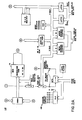
- Fig. 1 which depicts a display controller unit
- Fig. 2 which depicts in detail the picture processor 110 of Fig. 1
- a 100-pixel wide by 100- pixel high frame buffer is considered by way of example herein (Figs. 3-5), wherein it is intended that the top 80 lines of the total of 100 scan lines of the frame buffer are to be displayed on a screen, i.e., the displayed portion 20 of Figs. 3-5.
- a 20-pixel high by 100-pixel wide undisplayed strip at the bottom of the frame buffer 10 is thus available.
- a 50 by 50 pixel rectangle 25 is herein considered, as a representative shape to be filled-in by say a 7 by 3 pixel paint pattern.
- the geometric shape of a rectangle (or a square) is chosen for convenience in illustrating the invention. Indeed, virtually any predetermined area of desired shape may be rapidly' filled via this invention.
- Figs. 3-5 illustrate the upper left corner of the rectangle 25 as being positioned at point (30,20), in a left-handed coordinate system (0,0 in the upper left corner). A right- handed coordinate system could equally well be considered.
- the sample 7 x 3 pattern is initially loaded into the frame buffer, in this example at pixel locations 0-6 in X (horizontal dimension) and 80-82 in Y (vertical dimension). This is shown as rectangle 11 in Fig. 3.
- the pattern is then copied from there (or reloaded from the original pattern specification) to locations 7-13, 14-20, 21-27, etc. in X, all at 80-82 in Y.
- the entire width of the undisplayed portion 10 of the frame buffer is thus filled in this manner, as shown in Fig. 4.
- the final replication of the pattern, at 12, is truncated at the right edge of the screen, using only the left-two columns of the pattern definition, in this particular example.
- Other patterns may, of course, be entered into the remaining (unused) area of the undisplayed portion 10 of the frame buffer.
- each scan line of the section of the polygon may be a different width in a horizontal direction than the previous one (or even multiple sections along the same line).
- the proper scan line of the pattern store is copied to the appropriate section(s) of the polygon scan line, and the process repeated for the next line, just as for the rectangle.
- a principle advantage of this invention is the speed of filling-in areas. Except for special cases where the width of the pattern is an integer fraction of the frame buffer word width, copying a section of one scan line to a section of another scan line at the same horizontal position is much faster than replicating the pattern across the scan line section.
- the pattern was replicated across three full scan lines and then copied to 50 scan line sections, each 50 pixels wide. The alternative would have been to replicate the pattern across all 50 scan line sections.
- typical real frame buffer sizes with undisplayed portions may be 512 x 512 with 512 x 384 or 512 x 480 displayed, 640 x 512 with 640 x 480 displayed, 1024 x 1024 with 800 to 1024 x 600 to 1000 displayed, and 1280 x 1024 with 1280 x 960 to 990 displayed.
- the word width of typical real frame buffer implementations generally varies from 16 to 80.
- Fig. 1 in actuality shows a 1024 x 1024 pixel frame buffer built from 16-pixel words, whereas for the purposes of this example, there is assumed a 100 x 100 frame buffer built from 20-pixel words and 20- bit data paths throughout the picture processor and busses.
- Fig. 1 depicts monochrome operation, this invention is directly applicable to color arrangements.
- the microcode RAM 111 of the picture processor 110 is loaded with code capable of executing lists of commands (display lists) stored in memory in a so-called display processor unit (DPU).
- DPU display processor unit
- the local bus 120 connecting it with the display control unit (DCU) is shown in the lower left of Fig. 1.
- shadow register loop 130 is used for loading code.
- Commands in the display lists include ones to load paint patterns and ones to fill shapes (e. g . rectangles, general polygons, etc.), preferably with the most recently loaded pattern. Multiple areas filled with differing patterns can be drawn by interspersing load paint pattern commands with the fill area commands in a display list.
- the graphics illustrated in Fig. 6 are representative thereof.
- the picture processor 110 in executing a display list, will at some point encounter a load paint pattern command with say a 7 x 3 pixel pattern.
- the picture processor (pp) 110 reads the pattern and left-justifies it into three temporary registers (each 20 pixels wide to match the frame buffer word width). These registers, though not particularly shown, may be called A1, B1, and C1.
- the pp copies these registers into another register set, called say A2, B2, and C2, and shifts these to the right 7 places. It logically OR's A1 into A2, B1 into B2, and C1 into C2. The shifting and OR'ing is repeated once more to complete the first three words of the pattern store.
- the pp writes A2 into word 400, B2 into word 405, and C2 into word 410 of the frame buffer (the left word of scan lines 80, 81, and 82).
- the addresses for the write operations pass over the lines labelled LDA1-LDA23 and the data over lines LDDO-LDD19 (only LDDO-LD D 15 are shown in the diagram as it depicts a 16-pixel word width machine). These three words now each contain two complete copies of the pattern and a 6-pixel wide section of a third copy.
- a similar set of shift and OR operations is used to form the next set of three 20-pixel words, which are written to words 401, 406, and 411 of the frame buffer.
- This second set of three words will contain two complete copies of the pattern with an additional one-pixel wide section on the left (to complete the 6-pixel wide section at the right of the previous three words) and a 5-pixel wide section on the right.
- the remaining three sets of three words are each written in a similar manner.
- the pp completes the load paint pattern command by storing the height of the pattern, 3, in a word of local memory (or register) within the pp. This value is used later for the modulo and wrap around calculations.
- the pp will subsequently encounter the example command of: fill rectangle between 30,20 and 79;69.
- the pp uses the modulo calculation discussed previously, the pp calculates that the first pattern store scan line to be used is 82. It further calculates that the first (upper left) frame buffer word in the rectangle is 101 and that only the right 10 pixels of this word are within the rectangle.
- the pp reads the frame buffer words No. 101 and 411 (the word from line 82 of the pattern store directly under the word 101) into two temporary registers, say R1 and R2 respectively. It moves the right 10 pixels from R2 into R1 leaving the left ten pixels of R 1 unchanged, then writes R1 back into frame buffer word 101.
- frame buffer word 412 is read into a temporary register and immediately written to word 102, and word 413 similarly copied to word 103.
- a 50-pixel wide section of scan line 82 within the pattern store has now been copied into a 50-pixel section of scan line 20.
- the same procedure of reads and writes, except for different word addresses, is used to copy 50 pixels from scan line 80 into 21, line 81 into 22, 82 into 23, 80 into 24,..., 80 into 69. In this way, the entire rectangle becomes filled.
- More sophisticated frame buffers have the ability to write arbitrary sections of a word. In such cases moving 10 pixels from word 411 to 101 becomes a simple read and write, as would be the moves from 412 to 102 and 413 to 103 above.
- copying can be expanded to include logical operations between the source and destination. For example, a logical OR operation between the pattern store and the rectangle to fill results in a transparent pattern. Wherever there are zeros in the pattern store, the corresponding areas of the rectangle are left unchanged. This gives the appearance of seeing through the rectangle as if it were a screen door.
Landscapes
- Engineering & Computer Science (AREA)
- Physics & Mathematics (AREA)
- General Physics & Mathematics (AREA)
- Theoretical Computer Science (AREA)
- Computer Hardware Design (AREA)
- Image Generation (AREA)
- Controls And Circuits For Display Device (AREA)
- Digital Computer Display Output (AREA)
Abstract
Description
- This invention relates to graphics display units and more particularly to method and apparatus for rapidly filling predetermined areas of a graphics display screen. with predefined repetitive patterns which generally are relatively small in size compared to the total area to be filled with the pattern.
- The filling of such predetermined areas of a graphics display screen with one or more preselected patterns, of itself, is well known. Generally, however, existing arrangements are relatively quite slow in "painting" the patterns and require additional or special circuitry and storage capacity which add significantly to the cost of such displays. Moreover, in such arrangements replicating patterns generally involves considerable shifting, splitting, and partial word writes.
- What is needed is to be able to rapidly fill the predetermined areas of the screen without the requirement for substantial additional or special circuitry and memory and electronic manipulation required of prior art arrangements. According to the present invention, this problem is solved by effectively utilizing extra scan lines of the frame buffer memory, i.e., the lines of the frame buffer memory not being displayed on the screen, to house the patterns to be utilized in filling the predetermined shapes or areas, by first replicating those patterns as necessary in the undisplayed portion of the frame buffer memory, and utilizing portions of these stored patterns which coincide in at least one dimension with the shape(s) or area(s) to be filled, wherein the latter become filled one scan line at a time. Thereby, only the height of the patterns, as opposed to the areas to be filled-in per se, is required to fit in the height of the undisplayed section of the frame buffer.
- In accordance with the invention, therefore, there is provided a method for rapidly filling-in predetermined shapes or areas of a graphics display image with one or more predefined patterns, comprising:
- (a) . providing a frame buffer with a first section for receiving the information constituting the image to be displayed and a second section for receiving one or more patterns to be utilized in filling the predetermined shapes of the image being displayed;
- (b) defining at least one replicatable pattern to be utilized to fill said predetermined shapes;
- (c) entering the pattern information of said at least one pattern into said second section of the frame buffer;
- (d) replicating said pattern throughout the memory locations of said second section comprising the scan lines associated to the block of memory locations into which the pattern is entered initially; and
- (e) filling in one or more shapes of the image being displayed with said at least one predetermined pattern; replicated in said frame buffer second section.
- Also in accordance with the invention, there is provided apparatus for performing the aforementioned method which includes means for selecting a portion of the replicated pattern to fill a section of the shape to be filled such that said portion of the replicated pattern and said section of the shape coincide in at least one dimension of the frame buffer memory.
- Other advantages and features will become apparent, and the invention itself better understood, from the following detailed description, taken in conjunction with the accompanying drawings, in which:
- Fig. 1 is a block diagram of a graphics display's controller unit which includes the picture processor and frame buffer;
- Fig. 2 is a more detailed block diagram of the picture processor portion of Fig. 1;
- Figs. 3-5 are schematic representations of the frame buffer memory, illustrating the displayed and undisplayed sections and their relation to the filling of a sample area of the display screen with a preselected pattern; and
- Fig. 6 is an illustration demonstrating the pattern-filling capability of this invention in connection with overlapping screen areas.
- Referring to Fig. 1, which depicts a display controller unit, and Fig. 2 which depicts in detail the
picture processor 110 of Fig. 1, a 100-pixel wide by 100- pixel high frame buffer is considered by way of example herein (Figs. 3-5), wherein it is intended that the top 80 lines of the total of 100 scan lines of the frame buffer are to be displayed on a screen, i.e., the displayedportion 20 of Figs. 3-5. A 20-pixel high by 100-pixel wide undisplayed strip at the bottom of theframe buffer 10 is thus available. - Also by way of example, a 50 by 50
pixel rectangle 25 is herein considered, as a representative shape to be filled-in by say a 7 by 3 pixel paint pattern. The geometric shape of a rectangle (or a square) is chosen for convenience in illustrating the invention. Indeed, virtually any predetermined area of desired shape may be rapidly' filled via this invention. For ease of explanation, Figs. 3-5 illustrate the upper left corner of therectangle 25 as being positioned at point (30,20), in a left-handed coordinate system (0,0 in the upper left corner). A right- handed coordinate system could equally well be considered. - According to the invention, the sample 7 x 3 pattern is initially loaded into the frame buffer, in this example at pixel locations 0-6 in X (horizontal dimension) and 80-82 in Y (vertical dimension). This is shown as
rectangle 11 in Fig. 3. The pattern is then copied from there (or reloaded from the original pattern specification) to locations 7-13, 14-20, 21-27, etc. in X, all at 80-82 in Y. The entire width of theundisplayed portion 10 of the frame buffer is thus filled in this manner, as shown in Fig. 4. The final replication of the pattern, at 12, is truncated at the right edge of the screen, using only the left-two columns of the pattern definition, in this particular example. Other patterns may, of course, be entered into the remaining (unused) area of theundisplayed portion 10 of the frame buffer. - Having completed the preparatory phrase, the display unit may now actually fill the rectangle, one scan line at a time. This is done by copying, in this example, 50-pixel wide sections of the scan lines in the replicated pattern, from the undisplayed portion of the frame buffer, up into the rectangle. If the pattern is to align between adjacent rectangles, then the 50-pixel wide section of the pattern store used should be directly "under" the rectangle, and the top scan line of the rectangle should be filled from the line at (20 mod 3) + 80 = 82 in the pattern store. The next scan line of the rectangle should come from (21 mod 3) + 80 = 80 and so on. If pattern alignment between rectangles is not required, then the copying could always start with the top scan line of the pattern store and count down, resetting to the top scan line after every use of the bottom scan line of the replicated pattern.
- Where the example area being filled is a more general polygon, rather than simply a square or rectangle, the method of the invention still applies. The only change would be that each scan line of the section of the polygon may be a different width in a horizontal direction than the previous one (or even multiple sections along the same line). The proper scan line of the pattern store is copied to the appropriate section(s) of the polygon scan line, and the process repeated for the next line, just as for the rectangle.
- A principle advantage of this invention is the speed of filling-in areas. Except for special cases where the width of the pattern is an integer fraction of the frame buffer word width, copying a section of one scan line to a section of another scan line at the same horizontal position is much faster than replicating the pattern across the scan line section. In the example above, the pattern was replicated across three full scan lines and then copied to 50 scan line sections, each 50 pixels wide. The alternative would have been to replicate the pattern across all 50 scan line sections.
- While the 100 x 100 pixel frame buffer size for the within-described example was chosen for ease of illustration, typical real frame buffer sizes with undisplayed portions may be 512 x 512 with 512 x 384 or 512 x 480 displayed, 640 x 512 with 640 x 480 displayed, 1024 x 1024 with 800 to 1024 x 600 to 1000 displayed, and 1280 x 1024 with 1280 x 960 to 990 displayed. The word width of typical real frame buffer implementations generally varies from 16 to 80. Whereas replicating a pattern that is not an integer fraction of the word width generally involves much shifting, splitting, and partial word writes, with this invention copying from the pattern store requires no shifting and significantly fewer partial word writes, and can often be done with an entire frame buffer word per cycle.
- In connection with the example of the 100 x 100 pixel frame buffer herein described, one can consider an implementation of that frame buffer using, as example, 20-pixel memory words. Typically, one could assign memory words 0-4 to comprise scan line No. 0 (top), 5-9 for
scan line 1, etc., withwords 0, 5, etc on the left, andwords 4, 9, etc. on the right. The pixels within each word would be numbered from 0 on the left to 19 on the right. In this manner, the upper left pixel of the rectangle to be filled (30,20) would bepixel 10 of word 101, and the lower right pixel of the rectangle (79,69) would be No. 19 of word 348. - In discussing operation of the display control unit (DCU) depicted in Fig. 1 in connection with the filling of the 50 x 50 pixel example rectangle with the 7 x 3 pixel pattern, it is to be noted that Fig. 1 in actuality shows a 1024 x 1024 pixel frame buffer built from 16-pixel words, whereas for the purposes of this example, there is assumed a 100 x 100 frame buffer built from 20-pixel words and 20- bit data paths throughout the picture processor and busses. Moreover, although Fig. 1 depicts monochrome operation, this invention is directly applicable to color arrangements.
- During system initialization, the microcode RAM 111 of the
picture processor 110 is loaded with code capable of executing lists of commands (display lists) stored in memory in a so-called display processor unit (DPU). Although the DPU is not particularly shown in the figures, the local bus 120 connecting it with the display control unit (DCU) is shown in the lower left of Fig. 1. In this implementation,shadow register loop 130 is used for loading code. Commands in the display lists include ones to load paint patterns and ones to fill shapes (e.g. rectangles, general polygons, etc.), preferably with the most recently loaded pattern. Multiple areas filled with differing patterns can be drawn by interspersing load paint pattern commands with the fill area commands in a display list. The graphics illustrated in Fig. 6 are representative thereof. - It can be assumed, therefore, that the
picture processor 110 in executing a display list, will at some point encounter a load paint pattern command with say a 7 x 3 pixel pattern. The picture processor (pp) 110 reads the pattern and left-justifies it into three temporary registers (each 20 pixels wide to match the frame buffer word width). These registers, though not particularly shown, may be called A1, B1, and C1. The pp copies these registers into another register set, called say A2, B2, and C2, and shifts these to the right 7 places. It logically OR's A1 into A2, B1 into B2, and C1 into C2. The shifting and OR'ing is repeated once more to complete the first three words of the pattern store. The pp writes A2 into word 400, B2 into word 405, and C2 into word 410 of the frame buffer (the left word of scan lines 80, 81, and 82). The addresses for the write operations pass over the lines labelled LDA1-LDA23 and the data over lines LDDO-LDD19 (only LDDO-LDD15 are shown in the diagram as it depicts a 16-pixel word width machine). These three words now each contain two complete copies of the pattern and a 6-pixel wide section of a third copy. - A similar set of shift and OR operations is used to form the next set of three 20-pixel words, which are written to words 401, 406, and 411 of the frame buffer. This second set of three words will contain two complete copies of the pattern with an additional one-pixel wide section on the left (to complete the 6-pixel wide section at the right of the previous three words) and a 5-pixel wide section on the right. The remaining three sets of three words are each written in a similar manner. Having completed loading of the pattern store, the pp completes the load paint pattern command by storing the height of the pattern, 3, in a word of local memory (or register) within the pp. This value is used later for the modulo and wrap around calculations.
- The pp will subsequently encounter the example command of: fill rectangle between 30,20 and 79;69. Using the modulo calculation discussed previously, the pp calculates that the first pattern store scan line to be used is 82. It further calculates that the first (upper left) frame buffer word in the rectangle is 101 and that only the right 10 pixels of this word are within the rectangle. The pp reads the frame buffer words No. 101 and 411 (the word from line 82 of the pattern store directly under the word 101) into two temporary registers, say R1 and R2 respectively. It moves the right 10 pixels from R2 into R1 leaving the left ten pixels of R1 unchanged, then writes R1 back into frame buffer word 101. Next, frame buffer word 412 is read into a temporary register and immediately written to word 102, and word 413 similarly copied to
word 103. A 50-pixel wide section of scan line 82 within the pattern store has now been copied into a 50-pixel section ofscan line 20. The same procedure of reads and writes, except for different word addresses, is used to copy 50 pixels from scan line 80 into 21, line 81 into 22, 82 into 23, 80 into 24,..., 80 into 69. In this way, the entire rectangle becomes filled. - More sophisticated frame buffers have the ability to write arbitrary sections of a word. In such cases moving 10 pixels from word 411 to 101 becomes a simple read and write, as would be the moves from 412 to 102 and 413 to 103 above. An even faster frame buffer can be constructed tq provide for copying an arbitrary section of one scan line into the same section of another scan line as a single operation. In this case, the entire rectangle fill depicted herein would require only 50 operations. Without the present invention, filling this rectangle would require 8 x 50 = 400 writes of 7 or less pixels each, with shifting of the 7 pixels required on most of the writes.
- The operations described in this example all have the result of copying rectangular areas of pixels from one place to another. In the case of loading the paint pattern, it is copying a 7 x 3 pixel rectangle from the display list memory to multiple locations in the pattern store area of the frame buffer. In filling the rectangle, it is copying 50 x 1 pixel rectangles from the pattern store to the rectangle. For reference on copying rectangular pixel arrays, see Ingalls, D., "The Small Talk Graphics Kernel," special issue on Small Talk, BYTE, 6(8), August 1981. It again should be noted, however, that the patterning discussed in such article is restricted to 16- pixel wide patterns, which is the width of the frame buffer employed. It is referenced for rectangular area copying only, whereas the present invention provides more general patterning capability.
- As described in the BYTE article, copying can be expanded to include logical operations between the source and destination. For example, a logical OR operation between the pattern store and the rectangle to fill results in a transparent pattern. Wherever there are zeros in the pattern store, the corresponding areas of the rectangle are left unchanged. This gives the appearance of seeing through the rectangle as if it were a screen door.
- There has thus been described above a graphics display rapid pattern fill arrangement in which user- defined patterns within a delta X value and a delta Y value of frame buffer memory may be replicated in X from a "seed" memory location block in the undisplayed section of the frame buffer memory, until the desired portion of that frame buffer section (which may be the entire undisplayed section) is consumed, with coordinated portions of such replicated pattern being utilized to fill-in predetermined areas of the image to be displayed. In such arrangement, the boundary of the area or shape to be filled acts as a window to view the pattern and a replicated pattern will not actually be visible until the shape to be filled is drawn on the screen.
Claims (13)
Applications Claiming Priority (2)
| Application Number | Priority Date | Filing Date | Title |
|---|---|---|---|
| US06/647,955 US4646078A (en) | 1984-09-06 | 1984-09-06 | Graphics display rapid pattern fill using undisplayed frame buffer memory |
| US647955 | 1984-09-06 |
Publications (3)
| Publication Number | Publication Date |
|---|---|
| EP0174809A2 true EP0174809A2 (en) | 1986-03-19 |
| EP0174809A3 EP0174809A3 (en) | 1988-06-15 |
| EP0174809B1 EP0174809B1 (en) | 1991-11-13 |
Family
ID=24598893
Family Applications (1)
| Application Number | Title | Priority Date | Filing Date |
|---|---|---|---|
| EP85306322A Expired EP0174809B1 (en) | 1984-09-06 | 1985-09-05 | Graphics display rapid pattern fill using undisplayed frame buffer memory |
Country Status (5)
| Country | Link |
|---|---|
| US (1) | US4646078A (en) |
| EP (1) | EP0174809B1 (en) |
| JP (1) | JPS6167181A (en) |
| CA (1) | CA1241136A (en) |
| DE (1) | DE3584654D1 (en) |
Cited By (8)
| Publication number | Priority date | Publication date | Assignee | Title |
|---|---|---|---|---|
| EP0209736A2 (en) * | 1985-06-21 | 1987-01-28 | Hitachi, Ltd. | Display control device |
| EP0249285A1 (en) * | 1986-06-09 | 1987-12-16 | Océ-Nederland B.V. | A method of and a device for filling surface parts of an image with a surface pattern |
| EP0266431A1 (en) * | 1986-04-25 | 1988-05-11 | Fanuc Ltd. | Image processor |
| EP0322680A2 (en) * | 1987-12-25 | 1989-07-05 | Dainippon Screen Mfg. Co., Ltd. | Method of and apparatus for correcting color pattern in multicolor process |
| EP0354591A2 (en) * | 1988-08-12 | 1990-02-14 | Nec Corporation | Painting-out pattern reference system |
| EP0501814A2 (en) * | 1991-03-01 | 1992-09-02 | Canon Kabushiki Kaisha | Image processing apparatus |
| EP0673012A2 (en) * | 1994-03-11 | 1995-09-20 | Canon Information Systems Research Australia Pty Ltd. | Controller for a display with multiple common lines for each pixel |
| US6002385A (en) * | 1994-03-11 | 1999-12-14 | Canon Kabushiki Kaisha | Computer display system controller |
Families Citing this family (26)
| Publication number | Priority date | Publication date | Assignee | Title |
|---|---|---|---|---|
| US6552730B1 (en) * | 1984-10-05 | 2003-04-22 | Hitachi, Ltd. | Method and apparatus for bit operational process |
| US4754488A (en) * | 1984-12-07 | 1988-06-28 | International Business Machines Corporation | Method for ascertaining and filling of bounded areas of a colored raster display |
| US4853971A (en) * | 1985-03-18 | 1989-08-01 | Dainippon Screen Mfg. Co., Ltd. | Method and apparatus for processing image data |
| US5262767A (en) * | 1985-06-21 | 1993-11-16 | Hitachi, Ltd. | Display control device |
| US4791582A (en) * | 1985-09-27 | 1988-12-13 | Daikin Industries, Ltd. | Polygon-filling apparatus used in a scanning display unit and method of filling the same |
| JPS62192878A (en) * | 1986-02-20 | 1987-08-24 | Nippon Gakki Seizo Kk | Painting-out method for polygon |
| JP2610825B2 (en) * | 1986-04-16 | 1997-05-14 | キヤノン株式会社 | Graphic processing unit |
| US4788538A (en) * | 1986-11-17 | 1988-11-29 | Lotus Development Corporation | Method and apparatus for determining boundaries of graphic regions |
| US4988985A (en) * | 1987-01-30 | 1991-01-29 | Schlumberger Technology Corporation | Method and apparatus for a self-clearing copy mode in a frame-buffer memory |
| GB8704051D0 (en) * | 1987-02-20 | 1987-03-25 | Thermoteknix Systems Ltd | Printer control system |
| US5265214A (en) * | 1987-08-28 | 1993-11-23 | Daikin Industries, Ltd. | Filling processing apparatus and method |
| US4814884A (en) * | 1987-10-21 | 1989-03-21 | The United States Of America As Represented By The Secretary Of The Air Force | Window generator |
| US5357605A (en) * | 1988-09-13 | 1994-10-18 | Microsoft Corporation | Method and system for displaying patterns using a bitmap display |
| ES2110950T3 (en) * | 1988-11-14 | 1998-03-01 | Canon Kk | APPARATUS AND METHOD FOR IMAGE PROCESSING. |
| US5258750A (en) * | 1989-09-21 | 1993-11-02 | New Media Graphics Corporation | Color synchronizer and windowing system for use in a video/graphics system |
| US5146554A (en) * | 1989-09-29 | 1992-09-08 | Eastman Kodak Company | Page memory control in a raster image processor employed for digital halftoning |
| JPH04256080A (en) * | 1990-08-29 | 1992-09-10 | Xerox Corp | Method for converting protocol for expressing polygon |
| US5097256A (en) * | 1990-09-28 | 1992-03-17 | Xerox Corporation | Method of generating a cursor |
| GB9027678D0 (en) * | 1990-12-20 | 1991-02-13 | Ncr Co | Videographics display system |
| JP2647348B2 (en) * | 1993-09-20 | 1997-08-27 | インターナショナル・ビジネス・マシーンズ・コーポレイション | Clipping plane data storage system and method |
| US5454076A (en) * | 1994-03-02 | 1995-09-26 | Vlsi Technology, Inc. | Method and apparatus for simultaneously minimizing storage and maximizing total memory bandwidth for a repeating pattern |
| US5721565A (en) * | 1994-04-29 | 1998-02-24 | Proxima Corporation | Zooming protection display control system and method of using same |
| US5808691A (en) * | 1995-12-12 | 1998-09-15 | Cirrus Logic, Inc. | Digital carrier synthesis synchronized to a reference signal that is asynchronous with respect to a digital sampling clock |
| JP3809294B2 (en) * | 1999-03-31 | 2006-08-16 | 株式会社スクウェア・エニックス | GAME DEVICE, GAME METHOD, COMPUTER-READABLE RECORDING MEDIUM |
| US6483515B1 (en) * | 1999-04-09 | 2002-11-19 | Sun Microsystems, Inc. | Method and apparatus for displaying data patterns in information systems |
| JP5253348B2 (en) * | 2009-10-01 | 2013-07-31 | 三菱電機株式会社 | Status display device |
Family Cites Families (12)
| Publication number | Priority date | Publication date | Assignee | Title |
|---|---|---|---|---|
| US3696391A (en) * | 1969-09-19 | 1972-10-03 | Thomson Csf T Vt Sa | System for the display of synthesized graphic symbols |
| US3665410A (en) * | 1970-07-13 | 1972-05-23 | Bell Telephone Labor Inc | Computer graphics system with edge violation detection |
| US3778811A (en) * | 1972-06-21 | 1973-12-11 | Gte Sylvania Inc | Display system with graphic fill-in |
| FR2189870B1 (en) * | 1972-06-23 | 1977-06-17 | Thomson Csf | |
| SE423936B (en) * | 1980-01-16 | 1982-06-14 | Asea Ab | PROCEDURE FOR PRESENTING GRAPHIC INFORMATION AND DEVICE FOR IMPLEMENTATION OF THE PROCEDURE |
| US4317114A (en) * | 1980-05-12 | 1982-02-23 | Cromemco Inc. | Composite display device for combining image data and method |
| US4533911A (en) * | 1982-02-24 | 1985-08-06 | Daisy Systems Corporation | Video display system for displaying symbol-fragments in different orientations |
| US4524353A (en) * | 1982-03-29 | 1985-06-18 | Sperry Corporation | Line pattern template generator |
| US4528642A (en) * | 1982-04-12 | 1985-07-09 | Tektronix, Inc. | Completing a fill pattern inside a redrawn panel outline |
| JPS58191064A (en) * | 1982-04-30 | 1983-11-08 | Fujitsu Ltd | Face coating system of pattern |
| JPS5947665A (en) * | 1982-09-10 | 1984-03-17 | Alps Electric Co Ltd | Processing system of picture pattern |
| JPS5962892A (en) * | 1982-10-04 | 1984-04-10 | 三菱電機株式会社 | Graphic display unit |
-
1984
- 1984-09-06 US US06/647,955 patent/US4646078A/en not_active Expired - Lifetime
-
1985
- 1985-09-05 DE DE8585306322T patent/DE3584654D1/en not_active Expired - Fee Related
- 1985-09-05 EP EP85306322A patent/EP0174809B1/en not_active Expired
- 1985-09-05 CA CA000490023A patent/CA1241136A/en not_active Expired
- 1985-09-06 JP JP60197502A patent/JPS6167181A/en active Granted
Non-Patent Citations (3)
| Title |
|---|
| E.D.N. ELECTRICAL DESIGN NEWS, vol. 29, no. 11, 31st May 1984, pages 153-158,161,162,164,166,167,169,170, Boston, Massachusetts, US; M.S. YOUNG: "Use a CRT-controller chip to mix text and graphics" * |
| IEEE TRANSACTIONS ON COMPUTERS, vol. C-30, no. 1, January 1981, pages 41-47, New York, US; B.D. AGKLAND et al.: "The edge flag algorithm - a fill method for raster scan displays" * |
| MINI-MICRO CONFERENCE RECORD, May 1984, pages 1-8, Northeast, New York, US; J.C. DALRYMPLE et al.: "Display-processor architecture in the tektronix 4115B" * |
Cited By (17)
| Publication number | Priority date | Publication date | Assignee | Title |
|---|---|---|---|---|
| US5043717A (en) * | 1985-06-21 | 1991-08-27 | Hitachi, Ltd. | Display control device |
| EP0209736A2 (en) * | 1985-06-21 | 1987-01-28 | Hitachi, Ltd. | Display control device |
| EP0209736A3 (en) * | 1985-06-21 | 1990-05-02 | Hitachi, Ltd. | Display control device |
| EP0266431A1 (en) * | 1986-04-25 | 1988-05-11 | Fanuc Ltd. | Image processor |
| EP0266431A4 (en) * | 1986-04-25 | 1990-09-26 | Fanuc Ltd | Image processor |
| EP0249285A1 (en) * | 1986-06-09 | 1987-12-16 | Océ-Nederland B.V. | A method of and a device for filling surface parts of an image with a surface pattern |
| EP0322680A2 (en) * | 1987-12-25 | 1989-07-05 | Dainippon Screen Mfg. Co., Ltd. | Method of and apparatus for correcting color pattern in multicolor process |
| EP0322680A3 (en) * | 1987-12-25 | 1991-05-29 | Dainippon Screen Mfg. Co., Ltd. | Method of and apparatus for correcting color pattern in multicolor process |
| EP0354591A2 (en) * | 1988-08-12 | 1990-02-14 | Nec Corporation | Painting-out pattern reference system |
| EP0354591A3 (en) * | 1988-08-12 | 1992-01-02 | Nec Corporation | Painting-out pattern reference system |
| EP0501814A2 (en) * | 1991-03-01 | 1992-09-02 | Canon Kabushiki Kaisha | Image processing apparatus |
| EP0501814A3 (en) * | 1991-03-01 | 1993-03-10 | Canon Kabushiki Kaisha | Image processing apparatus |
| US5485288A (en) * | 1991-03-01 | 1996-01-16 | Canon Kabushiki Kaisha | Image processing apparatus for converting a color image into a pattern image with a synthesized gradation image increasing in density closer to contour portions of the pattern image |
| US5691827A (en) * | 1991-03-01 | 1997-11-25 | Canon Kabushiki Kaisha | Image processing apparatus for converting a color image into a pattern image with a line having a width which is equal to or less than a predetermined width not being converted |
| EP0673012A2 (en) * | 1994-03-11 | 1995-09-20 | Canon Information Systems Research Australia Pty Ltd. | Controller for a display with multiple common lines for each pixel |
| EP0673012A3 (en) * | 1994-03-11 | 1996-01-10 | Canon Information Syst Res | Controller for a display with multiple common lines for each pixel. |
| US6002385A (en) * | 1994-03-11 | 1999-12-14 | Canon Kabushiki Kaisha | Computer display system controller |
Also Published As
| Publication number | Publication date |
|---|---|
| JPS6167181A (en) | 1986-04-07 |
| DE3584654D1 (en) | 1991-12-19 |
| EP0174809B1 (en) | 1991-11-13 |
| EP0174809A3 (en) | 1988-06-15 |
| US4646078A (en) | 1987-02-24 |
| CA1241136A (en) | 1988-08-23 |
| JPH0431154B2 (en) | 1992-05-25 |
Similar Documents
| Publication | Publication Date | Title |
|---|---|---|
| US4646078A (en) | Graphics display rapid pattern fill using undisplayed frame buffer memory | |
| EP0104431B1 (en) | Image display system | |
| US4225861A (en) | Method and means for texture display in raster scanned color graphic | |
| US4559533A (en) | Method of electronically moving portions of several different images on a CRT screen | |
| EP0266506A2 (en) | Image display processor for graphics workstation | |
| EP0403121B1 (en) | Computer controlled screen animation | |
| EP0647931B1 (en) | High speed method and apparatus for generating animation by means of a three-region frame buffer and associated region pointers | |
| EP0139095A2 (en) | Display selection in a raster scan display system | |
| EP0887768B1 (en) | A graphic processor and a graphic processing method | |
| EP0191280B1 (en) | Bit adressable multidimensional array | |
| US4614941A (en) | Raster-scan/calligraphic combined display system for high speed processing of flight simulation data | |
| US4829292A (en) | Method for displaying box cursors | |
| US5977999A (en) | Electronic graphic apparatus with low data transfer rate between data stores | |
| JPH08211849A (en) | Display control device | |
| JPS63181074A (en) | Form depicting method | |
| EP0229986B1 (en) | Cursor circuit for a dual port memory | |
| JPH0242489A (en) | Picture display | |
| JPS6337388A (en) | Continuous image display system | |
| JPS59206889A (en) | Image processor | |
| JPH0435162A (en) | Partial moving device for still picture | |
| JP2867482B2 (en) | Image processing device | |
| JPS5836907B2 (en) | Superimposable color graphic display method | |
| JPS61273584A (en) | Display unit | |
| JPS61186992A (en) | Graphics display unit | |
| JPH1040412A (en) | Method and device for plotting three-dimensional graphic |
Legal Events
| Date | Code | Title | Description |
|---|---|---|---|
| PUAI | Public reference made under article 153(3) epc to a published international application that has entered the european phase |
Free format text: ORIGINAL CODE: 0009012 |
|
| AK | Designated contracting states |
Kind code of ref document: A2 Designated state(s): DE FR GB NL |
|
| PUAL | Search report despatched |
Free format text: ORIGINAL CODE: 0009013 |
|
| AK | Designated contracting states |
Kind code of ref document: A3 Designated state(s): DE FR GB NL |
|
| 17P | Request for examination filed |
Effective date: 19880801 |
|
| RAP1 | Party data changed (applicant data changed or rights of an application transferred) |
Owner name: TEKTRONIX, INC. |
|
| 17Q | First examination report despatched |
Effective date: 19901001 |
|
| GRAA | (expected) grant |
Free format text: ORIGINAL CODE: 0009210 |
|
| AK | Designated contracting states |
Kind code of ref document: B1 Designated state(s): DE FR GB NL |
|
| REF | Corresponds to: |
Ref document number: 3584654 Country of ref document: DE Date of ref document: 19911219 |
|
| ET | Fr: translation filed | ||
| PLBE | No opposition filed within time limit |
Free format text: ORIGINAL CODE: 0009261 |
|
| STAA | Information on the status of an ep patent application or granted ep patent |
Free format text: STATUS: NO OPPOSITION FILED WITHIN TIME LIMIT |
|
| 26N | No opposition filed | ||
| PGFP | Annual fee paid to national office [announced via postgrant information from national office to epo] |
Ref country code: FR Payment date: 19950803 Year of fee payment: 11 |
|
| PGFP | Annual fee paid to national office [announced via postgrant information from national office to epo] |
Ref country code: NL Payment date: 19950817 Year of fee payment: 11 |
|
| PG25 | Lapsed in a contracting state [announced via postgrant information from national office to epo] |
Ref country code: FR Effective date: 19960930 |
|
| PG25 | Lapsed in a contracting state [announced via postgrant information from national office to epo] |
Ref country code: NL Effective date: 19970401 |
|
| NLV4 | Nl: lapsed or anulled due to non-payment of the annual fee |
Effective date: 19970401 |
|
| REG | Reference to a national code |
Ref country code: FR Ref legal event code: ST |
|
| PGFP | Annual fee paid to national office [announced via postgrant information from national office to epo] |
Ref country code: GB Payment date: 19970815 Year of fee payment: 13 |
|
| PGFP | Annual fee paid to national office [announced via postgrant information from national office to epo] |
Ref country code: DE Payment date: 19970818 Year of fee payment: 13 |
|
| REG | Reference to a national code |
Ref country code: FR Ref legal event code: ST |
|
| PG25 | Lapsed in a contracting state [announced via postgrant information from national office to epo] |
Ref country code: GB Free format text: LAPSE BECAUSE OF NON-PAYMENT OF DUE FEES Effective date: 19980905 |
|
| GBPC | Gb: european patent ceased through non-payment of renewal fee |
Effective date: 19980905 |
|
| PG25 | Lapsed in a contracting state [announced via postgrant information from national office to epo] |
Ref country code: DE Free format text: LAPSE BECAUSE OF NON-PAYMENT OF DUE FEES Effective date: 19990701 |