EP0172694B1 - Optical receivers - Google Patents
Optical receivers Download PDFInfo
- Publication number
- EP0172694B1 EP0172694B1 EP85305520A EP85305520A EP0172694B1 EP 0172694 B1 EP0172694 B1 EP 0172694B1 EP 85305520 A EP85305520 A EP 85305520A EP 85305520 A EP85305520 A EP 85305520A EP 0172694 B1 EP0172694 B1 EP 0172694B1
- Authority
- EP
- European Patent Office
- Prior art keywords
- signal
- local oscillator
- cascode
- optical receiver
- optical
- Prior art date
- Legal status (The legal status is an assumption and is not a legal conclusion. Google has not performed a legal analysis and makes no representation as to the accuracy of the status listed.)
- Expired
Links
Images
Classifications
-
- H—ELECTRICITY
- H04—ELECTRIC COMMUNICATION TECHNIQUE
- H04B—TRANSMISSION
- H04B10/00—Transmission systems employing electromagnetic waves other than radio-waves, e.g. infrared, visible or ultraviolet light, or employing corpuscular radiation, e.g. quantum communication
- H04B10/60—Receivers
-
- H—ELECTRICITY
- H03—ELECTRONIC CIRCUITRY
- H03F—AMPLIFIERS
- H03F1/00—Details of amplifiers with only discharge tubes, only semiconductor devices or only unspecified devices as amplifying elements
- H03F1/08—Modifications of amplifiers to reduce detrimental influences of internal impedances of amplifying elements
- H03F1/22—Modifications of amplifiers to reduce detrimental influences of internal impedances of amplifying elements by use of cascode coupling, i.e. earthed cathode or emitter stage followed by earthed grid or base stage respectively
- H03F1/226—Modifications of amplifiers to reduce detrimental influences of internal impedances of amplifying elements by use of cascode coupling, i.e. earthed cathode or emitter stage followed by earthed grid or base stage respectively with junction-FET's
-
- H—ELECTRICITY
- H03—ELECTRONIC CIRCUITRY
- H03F—AMPLIFIERS
- H03F3/00—Amplifiers with only discharge tubes or only semiconductor devices as amplifying elements
- H03F3/04—Amplifiers with only discharge tubes or only semiconductor devices as amplifying elements with semiconductor devices only
- H03F3/08—Amplifiers with only discharge tubes or only semiconductor devices as amplifying elements with semiconductor devices only controlled by light
- H03F3/082—Amplifiers with only discharge tubes or only semiconductor devices as amplifying elements with semiconductor devices only controlled by light with FET's
-
- H—ELECTRICITY
- H04—ELECTRIC COMMUNICATION TECHNIQUE
- H04B—TRANSMISSION
- H04B10/00—Transmission systems employing electromagnetic waves other than radio-waves, e.g. infrared, visible or ultraviolet light, or employing corpuscular radiation, e.g. quantum communication
- H04B10/60—Receivers
- H04B10/61—Coherent receivers
- H04B10/64—Heterodyne, i.e. coherent receivers where, after the opto-electronic conversion, an electrical signal at an intermediate frequency [IF] is obtained
Definitions
- This invention relates to optical receivers, and in particular to pre-amplifier stages for optical receivers.
- optical transmission technology which calls for improved receivers, is coherent transmission technology which uses homodyne or heterodyne detection.
- Eden describes a preamp for use with avalanche photodiodes using a dual gate FET coupled to a single gate FET in cascade.
- the dual gate FET has its first gate coupled to the output of the APD, its second gate and source grounded, and its drain driving the gate of the single gate FET in a cascade arrangement.
- the source of the single gate FET is level-shifted and coupled by means of a feedback resistor to the first gate of the dual gate FET to provide a negative feedback.
- the output stage is a third FET with its gate coupled through a blocking capacitor to the source of the single gate FET in the input stage and with its drain providing the output of the preamp.
- the present invention aims to provide a pre-amplifier stage for an optical receiver which gives improved detection bandwidth when used for direct or coherent detection.
- the present invention aims to provide a pre-amplifier stage specially adapted for use with optical receivers capable of performing coherent heterodyne detection.
- a pre-amplifier stage comprising a first field effect transistor and a second transistor connected in cascode, and means to apply to the control electrode of the field effect transistor of the cascode an intermediate frequency (IF) signal obtained from mixing a received optical signal with a second optical signal, and means to apply to the control electrode of the second transistor of the cascode an electrical local oscillator signal.
- IF intermediate frequency
- the electrical local oscillator signal may be of nominally the same frequency as said IF signal, so that mixing with the electrical local oscillator results in demodulation of said IF signal and, hence, of the received signal.
- the electrical local oscillator signal may be of a frequency offset from the frequency of said IF signal, so that mixing of the electrical local oscillator signal with said IF signal results in a second IF signal.
- the local oscillator signal would be chosen such that the second IF is of much lower frequency than said, i.e. the first, IF signal, in order to reduce the bandwidth needed for subsequent signal processing circuits.
- the pre-amplifier of the optical heterodyne receiver preferably comprises a pre-amplifier according to the first aspect of the present invention.
- a first pre-amplifier stage of an optical receiver comprises a cascode circuit comprising a dual-gate field effect transistor.
- the dual-gate field effect transistor is preferably followed by a pre-amplifier output buffer stage comprising an field effect (FET) transistor.
- FET field effect
- the photo detector is preferably a PIN photo diode.
- the first pre-amplifier stage may also be used in combination with other photo detector devices, such as, for example, avalanche photo diodes (APDs).
- APDs avalanche photo diodes
- Replacing the conventionally used FET-bipolar transistor cascode circuit by a cascode circuit comprising a dual-gate FET has a number of advantages, the most important of which is that while employing device fabrication techniques of the same linewidth resolution in the as for conventional pre-amplifier circuits, the operating bandwidth of the pre-amplifier can be substantially increased. Another advantage is that a dual-gate device eases assembly of optical receivers because the number of bonding operations to the pre-amplifier is reduced. Thirdly, by using a further FET transistor in the output buffer stage, the whole pre-amplifier can readily be fabricated as a single integrated circuit device, which may, if desired, form part of a larger integrated circuit.
- the gate of the second stage of the cascode circuit may, for example, be connected to ground, or to a bias voltage supply.
- avalanche photo diode (APD) detectors in optical fibre communications systems operating in the range of 1-2 Gbit/s at wavelengths of 1.3 and 1.55 is known.
- APD avalanche photo diode
- the ternary compound In O . 53 Ga o . 47 As has a high absorption coefficient at both 1.3 and 1.55 micrometres, and receiver sensitivities of -37.5 and -38.1 dBm have been reported at these wavelengths using an InGaAs/InGaAsP/ InP avalanche photo diode at 1 Gbit/s transmission rates (c.f. J. C.
- indium gallium arsenide PIN photo diodes can, however, be exploited in conventional PIN FET hybrid optical receivers, and such receivers have already been demonstrated to have superior sensitivity, compared with Germanium APDs, at wavelengths of 1.3 and 1.5 micrometres and bit rates of up to 565 M/bts per second, and in addition have negligible temperature dependence and simple low voltage biasing requirements (c.f. "An experimental comparison of a germanium avalanche photo diode and indium gallium arsenide PIN FET receiver for longer wavelength optical communications systems, D. R. Smith, R. C. Hooper, P. P. Smith, D. Wake, Electronics Letters, Volume 18, No. 11, pages 453-454,1982). Until now, however, PIN FET receivers have not been practical for bit rates much in excess of 500 Mbit/s.
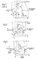
- FIG. 1 shows a circuit diagram of a photo detector and pre-amplifier of a typical known optical receiver comprising a PIN diode photo detector 1 which is optically coupled to an optical fibre 8, and a pre-amplifier 2.
- the pre-amplifier 2 consists of a first stage comprising an FET input transistor 3 connected in cascode with a bipolar transistor 4, and a pre-amplifier output stage 5 connected to the collector output of the bipolar transistor 4.
- the output stage consists of a bipolar emitter follower circuit.
- the PIN photo diode is an InGaAs PIN photo diode and the pre-amplifier configuration, by virtue of its high impedance, is an integrating amplifier.
- the maximum equalised bandwidth of this receiver is approximately 350 MHz allowing up to 650 Mbit/s operation.
- a circuit according to the invention has a pre-amplifier stage 12 comprising a dual-gate GaAs FET cascode circuit 10 comprising transistors 10' and 10", and a pre-amplifier output stage comprising an FET source follower 11.
- the dual-gate FET cascode is connected in series with a load resistor R L .
- the output from the load resistor R L is buffered by the source follower circuit 11 whose output is, in turn, coupled into a subsequent signal processing stage (not shown) from the source resistance R s .
- Dual-gate field effect transistors which may be said to consist essentially of two field effect transistors sharing a common device area which is the drain for one and the source for the other of the two transistors, are commercially available, and a description of such devices is therefore not considered necessary here.
- the circuit operates as follows.
- the photocurrent lp(t) injected in the photo diode 1 in response to an optical signal incident on the photo diode develops a signal voltage across the photo diode bias resistor R b which is applied to the gate of the first FET 10'.
- the bias resistor R b provides the return path for the photocurrent, and its bias voltage V b is controlled by an external feedback loop (not shown) to maintain the gate-to-source voltage Vgs of the transistor, and thereby keep the drain-to-source current I ds constant.
- the value of V gs is chosen to produce a value of I ds for minimum noise from the first FET 10', typically 0.151 dss (the saturated drain source current).
- the source follower 11 is used to buffer the output from the load resistor R L and provide a 50 Ohm or lower output impedance.
- the advantage of using a source follower for the pre-amplifier output stage is its very low input capacitance.
- Table 1 A comparison between the prior art circuit of Figure 1 and the circuit of Figure 2 is provided in Table 1, assuming a small area PIN photo diode with a diode capacitance C d of 0.1pF and a cascode load resistor of 560 Ohm.
- the pre-ampiifier lies at approximately 1.7 GHz, compared with a -3 dB point at only 570 MHz for the FET/bipolar pre-amplifier of the prior art with an emitter follower output buffer.
- the source follower has an order of magnitude less input capacitance than an emitter follower, and this lower capacitance contributes to allowing the extension of the -3dB point to the GHz range.
- a small geometry gate FET is required to achieve a low-frequency voltage gain ⁇ vLF closer to unity in order to reduce transmission loss and minimise input capacitance.
- the resulting lower value of the gate source capacitance Cg s will in turn lead to further reduction in the input capacitance.
- a heterodyne optical receiver employing the pre-amplifier circuit of Figure 2 has a received optical signal applied to the photo detector diode 1 together with an optical signal generated by an optical local oscillator U01.
- the local oscillator U01 provides a reference signal which, when mixed on the photo diode 1 with the received signal from optical fibre 8 results in a first intermediate frequency signal IF1.
- the first IF signal is applied to the gate of FET 10' of the cascode circuit 10', 10", and an electrical signal generated by local oscillator U02 is applied to the gate of the second of transistors 10', 10".
- the signal labelled IF2 is, in fact, the demodulated baseband signal from fibre 8.
- the frequency of the second local oscillator U02 differs from IF1
- another IF signal, IF2 is generated from the resulting mixing of IF1 and the output signal from U02.
Landscapes
- Engineering & Computer Science (AREA)
- Physics & Mathematics (AREA)
- Electromagnetism (AREA)
- Computer Networks & Wireless Communication (AREA)
- Signal Processing (AREA)
- Power Engineering (AREA)
- Optical Communication System (AREA)
- Amplifiers (AREA)
- Light Receiving Elements (AREA)
- Dc Digital Transmission (AREA)
- Glass Compositions (AREA)
- Surgical Instruments (AREA)
- Laser Surgery Devices (AREA)
Abstract
Description
- This invention relates to optical receivers, and in particular to pre-amplifier stages for optical receivers.
- Conventionally two kinds of photo detectors for optical receivers have been widely used for the detection of optically transmitted signals. For detection of data transmitted at bit rates up to a few hundred MHz, PIN diode photo detectors, followed by an FET-bipolar transistor cascode pre-amplifier, have generally been preferred because their device and circuit configuration are comparatively simple. However, for higher bit rates (1 GHz and above) avalanche photo diode (APD) detectors have been required, mainly because of their greater sensitivity on account of photo current gain, at the penalty of more complex device and circuit configurations.
- Improvements in optical transmitter technology, and in particular advances in the manufacture of low loss low dispersion optical fibre, and of narrow spectral line width laser sources, have led to the demonstration, in experimental systems, of transmission over optical fibers at bit rates well in excess of 1 Gbit/s, and further increases in transmission rates are to be expected. In order to exploit these high transmission rates in practical, commercial, optical fibre systems, receivers of commensurate bandwidth capability are required and, to enable fabrication and assembly costs to be kept as low as possible, these receivers should have as simple a structure as possible.
- A further development in optical transmission technology which calls for improved receivers, is coherent transmission technology which uses homodyne or heterodyne detection.
- In United States Patent US-A-4 075 576, Eden describes a preamp for use with avalanche photodiodes using a dual gate FET coupled to a single gate FET in cascade. The dual gate FET has its first gate coupled to the output of the APD, its second gate and source grounded, and its drain driving the gate of the single gate FET in a cascade arrangement. The source of the single gate FET is level-shifted and coupled by means of a feedback resistor to the first gate of the dual gate FET to provide a negative feedback. The output stage is a third FET with its gate coupled through a blocking capacitor to the source of the single gate FET in the input stage and with its drain providing the output of the preamp.
- The present invention aims to provide a pre-amplifier stage for an optical receiver which gives improved detection bandwidth when used for direct or coherent detection.
- Additionally, or alternatively, the present invention aims to provide a pre-amplifier stage specially adapted for use with optical receivers capable of performing coherent heterodyne detection.
- According to one aspect of the present invention, in an optical receiver a pre-amplifier stage comprising a first field effect transistor and a second transistor connected in cascode, and means to apply to the control electrode of the field effect transistor of the cascode an intermediate frequency (IF) signal obtained from mixing a received optical signal with a second optical signal, and means to apply to the control electrode of the second transistor of the cascode an electrical local oscillator signal.
- The electrical local oscillator signal may be of nominally the same frequency as said IF signal, so that mixing with the electrical local oscillator results in demodulation of said IF signal and, hence, of the received signal.
- Alternatively, the electrical local oscillator signal may be of a frequency offset from the frequency of said IF signal, so that mixing of the electrical local oscillator signal with said IF signal results in a second IF signal. Usually the local oscillator signal would be chosen such that the second IF is of much lower frequency than said, i.e. the first, IF signal, in order to reduce the bandwidth needed for subsequent signal processing circuits.
- The pre-amplifier of the optical heterodyne receiver preferably comprises a pre-amplifier according to the first aspect of the present invention.
- According to another aspect of the present invention, a first pre-amplifier stage of an optical receiver comprises a cascode circuit comprising a dual-gate field effect transistor.
- The dual-gate field effect transistor is preferably followed by a pre-amplifier output buffer stage comprising an field effect (FET) transistor.
- The photo detector is preferably a PIN photo diode.
- However, the first pre-amplifier stage may also be used in combination with other photo detector devices, such as, for example, avalanche photo diodes (APDs).
- Replacing the conventionally used FET-bipolar transistor cascode circuit by a cascode circuit comprising a dual-gate FET has a number of advantages, the most important of which is that while employing device fabrication techniques of the same linewidth resolution in the as for conventional pre-amplifier circuits, the operating bandwidth of the pre-amplifier can be substantially increased. Another advantage is that a dual-gate device eases assembly of optical receivers because the number of bonding operations to the pre-amplifier is reduced. Thirdly, by using a further FET transistor in the output buffer stage, the whole pre-amplifier can readily be fabricated as a single integrated circuit device, which may, if desired, form part of a larger integrated circuit.
- For direct detection applications, the gate of the second stage of the cascode circuit may, for example, be connected to ground, or to a bias voltage supply.
- The present invention will now be described further by way of example and with reference to the accompanying drawings of which:-
- Figure 1 is a schematic circuit diagram of a pre-amplifier of a commercially available optical receiver circuit;
- Figure 2 is a circuit diagram of a pre-amplifier in accordance with the present invention of an optical receiver for direct detection; and
- Figure 3 is a circuit diagram of the pre-amplifier of Figure 2 modified for coherent detection.
- To summarize the relevant background information, the use of avalanche photo diode (APD) detectors in optical fibre communications systems operating in the range of 1-2 Gbit/s at wavelengths of 1.3 and 1.55 is known. (c.f. Smith, D. R. et al, Electronics Letters, 1982, Volume 18, page 192-193). The ternary compound InO.53Gao.47As has a high absorption coefficient at both 1.3 and 1.55 micrometres, and receiver sensitivities of -37.5 and -38.1 dBm have been reported at these wavelengths using an InGaAs/InGaAsP/ InP avalanche photo diode at 1 Gbit/s transmission rates (c.f. J. C. Campbell et al, Electronics Letters 1983, Volume 19, pages 818-820.) However the need for a combination of low dark current, good frequency response and the required high gain-bandwidth product places conflicting design requirements on the structure of these devices making them extremely difficult to produce.
- The good responsivity of indium gallium arsenide PIN photo diodes can, however, be exploited in conventional PIN FET hybrid optical receivers, and such receivers have already been demonstrated to have superior sensitivity, compared with Germanium APDs, at wavelengths of 1.3 and 1.5 micrometres and bit rates of up to 565 M/bts per second, and in addition have negligible temperature dependence and simple low voltage biasing requirements (c.f. "An experimental comparison of a germanium avalanche photo diode and indium gallium arsenide PIN FET receiver for longer wavelength optical communications systems, D. R. Smith, R. C. Hooper, P. P. Smith, D. Wake, Electronics Letters, Volume 18, No. 11, pages 453-454,1982). Until now, however, PIN FET receivers have not been practical for bit rates much in excess of 500 Mbit/s.
- Referring now to Figure 1 which shows a circuit diagram of a photo detector and pre-amplifier of a typical known optical receiver comprising a PIN
diode photo detector 1 which is optically coupled to anoptical fibre 8, and a pre-amplifier 2. The pre-amplifier 2 consists of a first stage comprising an FET input transistor 3 connected in cascode with a bipolar transistor 4, and a pre-amplifier output stage 5 connected to the collector output of the bipolar transistor 4. The output stage consists of a bipolar emitter follower circuit. The PIN photo diode is an InGaAs PIN photo diode and the pre-amplifier configuration, by virtue of its high impedance, is an integrating amplifier. The maximum equalised bandwidth of this receiver is approximately 350 MHz allowing up to 650 Mbit/s operation. - Referring now to Figure 2, a circuit according to the invention has a
pre-amplifier stage 12 comprising a dual-gate GaAsFET cascode circuit 10 comprisingtransistors 10' and 10", and a pre-amplifier output stage comprising anFET source follower 11. The dual-gate FET cascode is connected in series with a load resistor RL. The output from the load resistor RL is buffered by thesource follower circuit 11 whose output is, in turn, coupled into a subsequent signal processing stage (not shown) from the source resistance Rs. Dual-gate field effect transistors, which may be said to consist essentially of two field effect transistors sharing a common device area which is the drain for one and the source for the other of the two transistors, are commercially available, and a description of such devices is therefore not considered necessary here. - The circuit operates as follows. The photocurrent lp(t) injected in the
photo diode 1 in response to an optical signal incident on the photo diode develops a signal voltage across the photo diode bias resistor Rb which is applied to the gate of the first FET 10'. The bias resistor Rb provides the return path for the photocurrent, and its bias voltage Vb is controlled by an external feedback loop (not shown) to maintain the gate-to-source voltage Vgs of the transistor, and thereby keep the drain-to-source current Ids constant. The value of Vgs is chosen to produce a value of Ids for minimum noise from the first FET 10', typically 0.151dss (the saturated drain source current). - The
source follower 11 is used to buffer the output from the load resistor RL and provide a 50 Ohm or lower output impedance. The advantage of using a source follower for the pre-amplifier output stage is its very low input capacitance. A comparison between the prior art circuit of Figure 1 and the circuit of Figure 2 is provided in Table 1, assuming a small area PIN photo diode with a diode capacitance Cd of 0.1pF and a cascode load resistor of 560 Ohm. The comparison is on the basis of employing the emitter follower 5 to the FET/bipolar cascode 3,4 of the prior art circuit of Figure 1, and thesource follower 11 to the FET/FET cascode 10', 10" of Figure 2, so that the performance of these output buffers can also be compared.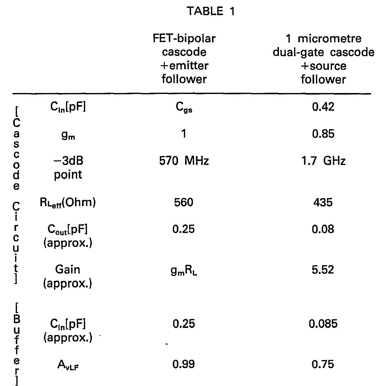
- the pre-ampiifier lies at approximately 1.7 GHz, compared with a -3 dB point at only 570 MHz for the FET/bipolar pre-amplifier of the prior art with an emitter follower output buffer.
- Higher transconductance and lower input capacitance are obtainable from FETs with smaller gate length, so that receiver sensitivities obtained from the 1 micrometre gate length FET can be yet further improved, and In addition the higher voltage gain of smaller geometry devices will help to offset second stage noise penalties.
- The source follower has an order of magnitude less input capacitance than an emitter follower, and this lower capacitance contributes to allowing the extension of the -3dB point to the GHz range. A small geometry gate FET is required to achieve a low-frequency voltage gain ÄvLF closer to unity in order to reduce transmission loss and minimise input capacitance. The resulting lower value of the gate source capacitance Cgs will in turn lead to further reduction in the input capacitance.
- Referring now to Figure 3, a heterodyne optical receiver employing the pre-amplifier circuit of Figure 2 has a received optical signal applied to the
photo detector diode 1 together with an optical signal generated by an optical local oscillator U01. The local oscillator U01 provides a reference signal which, when mixed on thephoto diode 1 with the received signal fromoptical fibre 8 results in a first intermediate frequency signal IF1. - The first IF signal is applied to the gate of FET 10' of the
cascode circuit 10', 10", and an electrical signal generated by local oscillator U02 is applied to the gate of the second oftransistors 10', 10". If the frequency of the first IF signal IF1 is the same as that of the local oscillator LO/2, then the signal labelled IF2 is, in fact, the demodulated baseband signal fromfibre 8. However, if the frequency of the second local oscillator U02 differs from IF1, then another IF signal, IF2, is generated from the resulting mixing of IF1 and the output signal from U02. - In summary, by applying to the second stage of a cascode pre-amplifier an electrical local oscillator signal, it is possible to operate the receiver either in a heterodyne-heterodyne mode, or in a heterodyne-homodyne mode, depending on the frequency relationship between the local oscillator generated signal and the IF signal IF1.
Claims (12)
Priority Applications (1)
| Application Number | Priority Date | Filing Date | Title |
|---|---|---|---|
| AT85305520T ATE46235T1 (en) | 1984-08-03 | 1985-08-02 | OPTICAL RECEIVER. |
Applications Claiming Priority (2)
| Application Number | Priority Date | Filing Date | Title |
|---|---|---|---|
| GB8419843 | 1984-08-03 | ||
| GB848419843A GB8419843D0 (en) | 1984-08-03 | 1984-08-03 | Optical receivers |
Publications (2)
| Publication Number | Publication Date |
|---|---|
| EP0172694A1 EP0172694A1 (en) | 1986-02-26 |
| EP0172694B1 true EP0172694B1 (en) | 1989-09-06 |
Family
ID=10564895
Family Applications (1)
| Application Number | Title | Priority Date | Filing Date |
|---|---|---|---|
| EP85305520A Expired EP0172694B1 (en) | 1984-08-03 | 1985-08-02 | Optical receivers |
Country Status (8)
| Country | Link |
|---|---|
| US (1) | US4750217A (en) |
| EP (1) | EP0172694B1 (en) |
| JP (1) | JPH06105855B2 (en) |
| AT (1) | ATE46235T1 (en) |
| CA (1) | CA1246678A (en) |
| DE (1) | DE3572902D1 (en) |
| GB (1) | GB8419843D0 (en) |
| WO (1) | WO1986001353A1 (en) |
Cited By (1)
| Publication number | Priority date | Publication date | Assignee | Title |
|---|---|---|---|---|
| CN103888084A (en) * | 2014-03-25 | 2014-06-25 | 中国科学院空间科学与应用研究中心 | Integrated pre-amplifier used for charged particle detector |
Families Citing this family (31)
| Publication number | Priority date | Publication date | Assignee | Title |
|---|---|---|---|---|
| DE3623135A1 (en) * | 1986-07-09 | 1988-01-28 | Telefunken Electronic Gmbh | Optical amplifier |
| GB2194111A (en) * | 1986-07-18 | 1988-02-24 | Gen Electric Plc | Optical signal receiver circuits |
| US4881044A (en) * | 1987-01-16 | 1989-11-14 | Hitachi, Ltd. | Amplifying circuit |
| DE8714248U1 (en) * | 1987-10-26 | 1989-02-23 | Heimann Optoelectronics Gmbh, 65199 Wiesbaden | Infrared detector |
| US4868894A (en) * | 1987-12-09 | 1989-09-19 | United Technologies | System for transmitting microwave signals via an optical link |
| DE3806283A1 (en) * | 1988-02-27 | 1989-09-07 | Telefunken Electronic Gmbh | OPTOELECTRONIC TRANSIMPEDANCE AMPLIFIER |
| DE3818168A1 (en) * | 1988-05-26 | 1990-04-05 | Krone Ag | RECEIVER PRE-AMPLIFIER FOR AN OPTICAL MESSAGE RANGE |
| US5254957A (en) * | 1989-01-04 | 1993-10-19 | Information Storage, Inc. | Apparatus and method for amplifying optically sensed signals |
| JPH0340533A (en) * | 1989-07-06 | 1991-02-21 | Sumitomo Electric Ind Ltd | Demodulation circuit |
| US5347388A (en) * | 1989-12-01 | 1994-09-13 | Scientific-Atlanta, Inc. | Push-pull optical receiver having gain control |
| US5239402A (en) * | 1989-12-01 | 1993-08-24 | Scientific-Atlanta, Inc. | Push-pull optical receiver |
| US4998012A (en) * | 1989-12-01 | 1991-03-05 | Scientific Atlanta, Inc. | Fiber optic transimpedance receiver |
| US5267071A (en) * | 1991-09-03 | 1993-11-30 | Scientific-Atlanta, Inc. | Signal level control circuitry for a fiber communications system |
| FR2684506A1 (en) * | 1991-11-29 | 1993-06-04 | Thomson Composants Militaires | LIGHT SIGNAL RECEIVER. |
| JP3080472B2 (en) * | 1992-03-24 | 2000-08-28 | 大川 彰一 | Preamplifier for radiation detection |
| US5280335A (en) * | 1992-05-26 | 1994-01-18 | The United States Of America As Represented By The Secretary Of The Navy | Fiber-optical testing system having a detection circuit |
| JP2843477B2 (en) * | 1993-03-18 | 1999-01-06 | 富士通株式会社 | Optical signal input type amplifier circuit |
| US5450227A (en) * | 1993-05-03 | 1995-09-12 | The United States Of America As Represented By The Secretary Of The Army | Optically injection-locked self-oscillating dual-gate MESFET mixer |
| US5347389A (en) * | 1993-05-27 | 1994-09-13 | Scientific-Atlanta, Inc. | Push-pull optical receiver with cascode amplifiers |
| JPH07245540A (en) * | 1994-01-12 | 1995-09-19 | Fujitsu Ltd | Optical receiver for optical digital communication |
| US5663639A (en) * | 1994-01-18 | 1997-09-02 | Massachusetts Institute Of Technology | Apparatus and method for optical heterodyne conversion |
| JPH08509350A (en) * | 1994-02-18 | 1996-10-01 | フィリップス、エレクトロニクス、ネムローゼ、フェンノートシャップ | Wideband multiplicative characteristic detector having triangular frequency characteristic, and transmission system and receiver including the detector |
| JP2713224B2 (en) * | 1995-05-01 | 1998-02-16 | 日本電気株式会社 | Optical receiver |
| US7475098B2 (en) * | 2002-03-19 | 2009-01-06 | Network Appliance, Inc. | System and method for managing a plurality of snapshots |
| US7002131B1 (en) | 2003-01-24 | 2006-02-21 | Jds Uniphase Corporation | Methods, systems and apparatus for measuring average received optical power |
| US7215883B1 (en) | 2003-01-24 | 2007-05-08 | Jds Uniphase Corporation | Methods for determining the performance, status, and advanced failure of optical communication channels |
| EP1445922A1 (en) * | 2003-02-06 | 2004-08-11 | Dialog Semiconductor GmbH | Monolithic optical read-out circuit |
| WO2006069358A2 (en) * | 2004-12-22 | 2006-06-29 | Enterprise Integration Group | Turn-taking model |
| AU2009291495A1 (en) * | 2008-09-11 | 2010-03-18 | Savage, Paul | Low distortion cascode amplifier circuit |
| FR2988239A1 (en) * | 2012-03-16 | 2013-09-20 | Converteam Technology Ltd | METHOD FOR COMPENSATING TOLERANCES FOR MANUFACTURING AT LEAST ONE ELECTRIC PARAMETER OF A POWER TRANSISTOR AND SYSTEM THEREOF |
| JP2015012540A (en) * | 2013-07-01 | 2015-01-19 | 株式会社東芝 | Light receiving circuit |
Family Cites Families (3)
| Publication number | Priority date | Publication date | Assignee | Title |
|---|---|---|---|---|
| CA1024239A (en) * | 1972-04-17 | 1978-01-10 | Rca Limited | Low noise detector amplifier |
| US4075576A (en) | 1977-02-25 | 1978-02-21 | Rockwell International Corporation | Sensitive high speed solid state preamp |
| US4380828A (en) * | 1981-05-26 | 1983-04-19 | Zenith Radio Corporation | UHF MOSFET Mixer |
-
1984
- 1984-08-03 GB GB848419843A patent/GB8419843D0/en active Pending
-
1985
- 1985-08-01 CA CA000488000A patent/CA1246678A/en not_active Expired
- 1985-08-02 WO PCT/GB1985/000346 patent/WO1986001353A1/en not_active Ceased
- 1985-08-02 DE DE8585305520T patent/DE3572902D1/en not_active Expired
- 1985-08-02 EP EP85305520A patent/EP0172694B1/en not_active Expired
- 1985-08-02 AT AT85305520T patent/ATE46235T1/en not_active IP Right Cessation
- 1985-08-02 JP JP60503458A patent/JPH06105855B2/en not_active Expired - Lifetime
- 1985-08-02 US US06/849,515 patent/US4750217A/en not_active Expired - Fee Related
Cited By (2)
| Publication number | Priority date | Publication date | Assignee | Title |
|---|---|---|---|---|
| CN103888084A (en) * | 2014-03-25 | 2014-06-25 | 中国科学院空间科学与应用研究中心 | Integrated pre-amplifier used for charged particle detector |
| CN103888084B (en) * | 2014-03-25 | 2016-08-24 | 中国科学院空间科学与应用研究中心 | A kind of integrated preamplifier for charged particle detector |
Also Published As
| Publication number | Publication date |
|---|---|
| GB8419843D0 (en) | 1984-09-05 |
| WO1986001353A1 (en) | 1986-02-27 |
| EP0172694A1 (en) | 1986-02-26 |
| DE3572902D1 (en) | 1989-10-12 |
| CA1246678A (en) | 1988-12-13 |
| JPS61502929A (en) | 1986-12-11 |
| JPH06105855B2 (en) | 1994-12-21 |
| US4750217A (en) | 1988-06-07 |
| ATE46235T1 (en) | 1989-09-15 |
Similar Documents
| Publication | Publication Date | Title |
|---|---|---|
| US4750217A (en) | Optical receivers | |
| US6275114B1 (en) | Impedance matched CMOS transimpedance amplifier for high-speed fiber optic communications | |
| US5646573A (en) | Automatic gain-control transimpedence amplifier | |
| EP0568880B1 (en) | Preamplifier for optical communication having a gain control circuit | |
| EP0108792B1 (en) | Fet amplifier with wide dynamic range | |
| US4075576A (en) | Sensitive high speed solid state preamp | |
| US6879217B2 (en) | Triode region MOSFET current source to bias a transimpedance amplifier | |
| Ikeda et al. | An auto-gain control transimpedance amplifier with low noise and wide input dynamic range for 10-Gb/s optical communication systems | |
| JPH0783313B2 (en) | Front end for broadband optical receiver | |
| US4647762A (en) | Optical receiver | |
| EP0579751B1 (en) | Differential transimpedance amplifier | |
| US6876260B2 (en) | Elevated front-end transimpedance amplifier | |
| CA2123667C (en) | Opto-electronic integrated circuit | |
| US6844784B1 (en) | Wide dynamic range transimpedance amplifier | |
| US4638152A (en) | Photoelectric converting circuit having a low parasitic capacitance | |
| Hamaguchi et al. | GaAs optoelectronic integrated receiver with high-output fast-response characteristics | |
| Williams et al. | Active feedback lightwave receivers | |
| Lao et al. | 20-Gb/s 14-k/spl Omega/transimpedance long-wavelength MSM-HEMT photoreceiver OEIC | |
| Sibley et al. | The design of pin-bipolar transimpedance pre-amplifiers for optical receivers | |
| GB2135551A (en) | Optical receivers | |
| CA2060689C (en) | Optical control circuit for a microwave monolithic integrated circuit | |
| Liong et al. | Calculated signal-noise ratio of the combination of a PIN photodiode and a distributed amplifier with frequency dependent characteristic impedances | |
| RU2058661C1 (en) | Photo current amplifier | |
| JPS62217738A (en) | Optical reception circuit | |
| Schwaderer | PIN-FET preamplifier for high-speed optical transmission systems |
Legal Events
| Date | Code | Title | Description |
|---|---|---|---|
| PUAI | Public reference made under article 153(3) epc to a published international application that has entered the european phase |
Free format text: ORIGINAL CODE: 0009012 |
|
| AK | Designated contracting states |
Designated state(s): AT BE CH DE FR GB IT LI LU NL SE |
|
| 17P | Request for examination filed |
Effective date: 19860728 |
|
| 17Q | First examination report despatched |
Effective date: 19880316 |
|
| RAP1 | Party data changed (applicant data changed or rights of an application transferred) |
Owner name: BRITISH TELECOMMUNICATIONS PUBLIC LIMITED COMPANY |
|
| GRAA | (expected) grant |
Free format text: ORIGINAL CODE: 0009210 |
|
| AK | Designated contracting states |
Kind code of ref document: B1 Designated state(s): AT BE CH DE FR GB IT LI LU NL SE |
|
| REF | Corresponds to: |
Ref document number: 46235 Country of ref document: AT Date of ref document: 19890915 Kind code of ref document: T |
|
| ITF | It: translation for a ep patent filed | ||
| REF | Corresponds to: |
Ref document number: 3572902 Country of ref document: DE Date of ref document: 19891012 |
|
| ET | Fr: translation filed | ||
| PLBE | No opposition filed within time limit |
Free format text: ORIGINAL CODE: 0009261 |
|
| STAA | Information on the status of an ep patent application or granted ep patent |
Free format text: STATUS: NO OPPOSITION FILED WITHIN TIME LIMIT |
|
| 26N | No opposition filed | ||
| ITTA | It: last paid annual fee | ||
| EPTA | Lu: last paid annual fee | ||
| PGFP | Annual fee paid to national office [announced via postgrant information from national office to epo] |
Ref country code: FR Payment date: 19940711 Year of fee payment: 10 |
|
| PGFP | Annual fee paid to national office [announced via postgrant information from national office to epo] |
Ref country code: CH Payment date: 19940714 Year of fee payment: 10 Ref country code: AT Payment date: 19940714 Year of fee payment: 10 |
|
| PGFP | Annual fee paid to national office [announced via postgrant information from national office to epo] |
Ref country code: DE Payment date: 19940720 Year of fee payment: 10 |
|
| PGFP | Annual fee paid to national office [announced via postgrant information from national office to epo] |
Ref country code: BE Payment date: 19940728 Year of fee payment: 10 |
|
| PGFP | Annual fee paid to national office [announced via postgrant information from national office to epo] |
Ref country code: LU Payment date: 19940801 Year of fee payment: 10 |
|
| PGFP | Annual fee paid to national office [announced via postgrant information from national office to epo] |
Ref country code: SE Payment date: 19940831 Year of fee payment: 10 Ref country code: NL Payment date: 19940831 Year of fee payment: 10 |
|
| EAL | Se: european patent in force in sweden |
Ref document number: 85305520.0 |
|
| PG25 | Lapsed in a contracting state [announced via postgrant information from national office to epo] |
Ref country code: LU Free format text: LAPSE BECAUSE OF NON-PAYMENT OF DUE FEES Effective date: 19950802 Ref country code: AT Effective date: 19950802 |
|
| PG25 | Lapsed in a contracting state [announced via postgrant information from national office to epo] |
Ref country code: SE Effective date: 19950803 |
|
| PG25 | Lapsed in a contracting state [announced via postgrant information from national office to epo] |
Ref country code: LI Effective date: 19950831 Ref country code: CH Effective date: 19950831 Ref country code: BE Effective date: 19950831 |
|
| BERE | Be: lapsed |
Owner name: BRITISH TELECOMMUNICATIONS P.L.C. Effective date: 19950831 |
|
| PG25 | Lapsed in a contracting state [announced via postgrant information from national office to epo] |
Ref country code: NL Effective date: 19960301 |
|
| REG | Reference to a national code |
Ref country code: CH Ref legal event code: PL |
|
| PG25 | Lapsed in a contracting state [announced via postgrant information from national office to epo] |
Ref country code: FR Effective date: 19960430 |
|
| NLV4 | Nl: lapsed or anulled due to non-payment of the annual fee |
Effective date: 19960301 |
|
| PG25 | Lapsed in a contracting state [announced via postgrant information from national office to epo] |
Ref country code: DE Effective date: 19960501 |
|
| EUG | Se: european patent has lapsed |
Ref document number: 85305520.0 |
|
| REG | Reference to a national code |
Ref country code: FR Ref legal event code: ST |
|
| PGFP | Annual fee paid to national office [announced via postgrant information from national office to epo] |
Ref country code: GB Payment date: 19980721 Year of fee payment: 14 |
|
| PG25 | Lapsed in a contracting state [announced via postgrant information from national office to epo] |
Ref country code: GB Free format text: LAPSE BECAUSE OF NON-PAYMENT OF DUE FEES Effective date: 19990802 |
|
| GBPC | Gb: european patent ceased through non-payment of renewal fee |
Effective date: 19990802 |