EP0170971A2 - Verfahren zur Verteilung der Leitungsbelastung auf einer Schaltkarte oder auf einem Verbindungspackage mit jeweils mehreren Verdrahtungsebenen - Google Patents
Verfahren zur Verteilung der Leitungsbelastung auf einer Schaltkarte oder auf einem Verbindungspackage mit jeweils mehreren Verdrahtungsebenen Download PDFInfo
- Publication number
- EP0170971A2 EP0170971A2 EP85109188A EP85109188A EP0170971A2 EP 0170971 A2 EP0170971 A2 EP 0170971A2 EP 85109188 A EP85109188 A EP 85109188A EP 85109188 A EP85109188 A EP 85109188A EP 0170971 A2 EP0170971 A2 EP 0170971A2
- Authority
- EP
- European Patent Office
- Prior art keywords
- layer
- net
- layers
- connections
- connection
- Prior art date
- Legal status (The legal status is an assumption and is not a legal conclusion. Google has not performed a legal analysis and makes no representation as to the accuracy of the status listed.)
- Granted
Links
Images

Classifications
-
- G—PHYSICS
- G06—COMPUTING OR CALCULATING; COUNTING
- G06F—ELECTRIC DIGITAL DATA PROCESSING
- G06F30/00—Computer-aided design [CAD]
- G06F30/30—Circuit design
- G06F30/39—Circuit design at the physical level
- G06F30/394—Routing
-
- H—ELECTRICITY
- H05—ELECTRIC TECHNIQUES NOT OTHERWISE PROVIDED FOR
- H05K—PRINTED CIRCUITS; CASINGS OR CONSTRUCTIONAL DETAILS OF ELECTRIC APPARATUS; MANUFACTURE OF ASSEMBLAGES OF ELECTRICAL COMPONENTS
- H05K3/00—Apparatus or processes for manufacturing printed circuits
- H05K3/0005—Apparatus or processes for manufacturing printed circuits for designing circuits by computer
Definitions
- the invention relates to a method of assigning electrical connections to the several layers of a multilayer interconnection package to effect a distribution of the electrical connections. More particularly, the invention relates to a method for distributing electrical connections among the layers of a multilayer interconnection package, in such a manner that the number of connections passing through each region of the package is evenly balanced among all the layers, and such that each connection or each net, comprising one or more connections, is assigned to a single layer.
- connection The electrical connection of individual components on large or very large scale integrated circuits and interconnection packages is achieved using metallic paths between the endpoints (or pins) which are to be connected.
- a path between two pins is referred to as a connection.
- a net is a specified set of one or more connections.
- the connections of a net are all electrically in common; that is, there is a path joining any two pins of the net, either directly or by means of other pins of the net.
- the method of the present invention does not, however, require this property of electrical commonality.
- the present invention is concerned with packages that contain more than one wiring layer and that are designed so that each connection is required to be routed completely within one of the layers. That is, the path for a connection passes from one pin, down to a wiring layer, then to a point beneath the other pin, still within the same wiring layer, then to the other pin.
- a layer typically, but not necessarily, comprises a pair of wiring planes, often referred to as 'x' and 'y' planes when the predominant direction of wiring within each plane of the layer is disposed along orthogonal 'x' and 'y' axes respectively.
- the present invention provides a method that assigns each connection to a layer in such a way that wire load in each region (number and length of connactions passing through the region) is evenly balanced among the layers of the package. ('Region' means a portion of the package that comprises all layers, but is limited in areal extent in the x-y plane.)
- the present invention also provides a method for making such an assignment while providing evenly balanced wire load in each region of the package.
- One method is to use a sequential routing procedure. In such a method, one attempts to route a connection in a first layer without violating package design rules. If this fails, one attempts to route the connection in a second layer, etc. until a valid routing is found or the connection fails to be routed. One then proceeds to the next required connection. This can result in an imbalance between the number (and total length) of connection paths on the several layers, which can lead to a requirement for more wiring layers than would be the case according to the method of the present invention.
- a second method is to randomly assign each connection to some layer, so that each connection has an equal probability of being assigned to any of the layers.
- This method results in regional imbalances of wire load among the layers, due to statistical fluctuations.
- N The average number of wires traversing the region in each layer
- N/L The average number of wires traversing the region in each layer
- N the actual number of wires in each layer will deviate from N/L by a number on the order of the square root of (N/L), because of statistical fluctuations.
- N the number of wires connecting pins that lie in two specified regions.
- the present invention distributes connections among layers in such a way that the number of connections between pins that lie in two specified regions is evenly balanced among the layers, without such statistical fluctuations.
- the aspect of that invention that relates to assignment of connections to layers comprises a method of initially randomly assigning to each connection a layer and an initial approximate wire routing (referred to as a global routing), then iteratively removing and rerouting each connection in turn so as to determine a new routing (and layer assignment) that minimizes certain undesirable routing characteristics at each iterative step.
- a global routing an initial approximate wire routing
- the method of the present invention does not require that a wire routing be performed in order to determine layer assignments. Furthermore, the present invention can be used to assign connections to layers with resulting balanced wire load in each region of the package, even when all connections of each net are required to be assigned to the same layer.
- European Patent Application publication number 78388 describes a methof of optimizing a required organization of many discrete elements and in the
- An aspect of the present invention relates to the making of a decision on a probabilistic basis, for the case in which all connections of each net must be assigned to the same layer. While this decision can be made using a random number and a T-value that decreases gradually during the process, this is not required.
- connection or net assignment teaches the use of 'connection type' classes as a means for balancing wire load among layers; the prior art method does not relate to these issues.
- the wiring load in each region of a multilayer interconnection package is balanced among all layers.
- Each net or other desired subset of two-pin connections is assigned to a single layer.
- the first of the above-mentioned features improves package wire- ability, while the second is useful or necessary for (a) satisfying certain package technology constraints, (b) improving design efficiency, and (c) improving electrical performance.
- connection types are defined in such a way that two connections are of the same connection type if, and only if, the pins of one connection are located within the same regions of the package as are the pins of the other connection.
- connection types in this way provides a means for balancing wire load effectively, in advance of any actual approximate or exact wire routing.
- Figure la shows a four-by-four global grid defined on an interconnection package.
- the global grid has 16 cells in it, numbered 1 through 16.
- a first connection AB connects a pin A in cell 5 with a pin B in cell 11.
- connections will be defined by referring to the lower number or earlier in sequence letter first. Assuming in this example that the connection types are referred to by cell number, the lower cell number is listed first according to the convention.
- connection AB may be referred to as a connection type (5, 11).
- connection type (5, 11) is the same as connection type (11, 5) but both are referred to as connection type (5, 11).
- connection CD is shown within cell 4. This will be referred to as a connection type (4, 4). In contrast to the (5, 11) connection type made between two differently-numbered cells, this connection is made within a single cell.
- the problem is regarded as one of balancing connection types among the layers, subject to the constraint that all connections of a net must be assigned to the same layer.
- connection type in terms of the global cells in which the pins of the connection are located
- connection type in terms of other regions, arbitrarily disposed on the package, in which the pins are located.
- One useful choice is to define the connection type in terms of the components mounted on the package with which the pins of the connection are associated.
- Table I illustrates the determination of connection type, given a connection list each connection of which is labeled by a 'NETNAME' and by a pair of connection pins. For this illustration, it is assumed that each pin has a letter-number designation, the letter specifying the name of the component with which the pin is associated, and the number labeling a particular pin associated with that component. There are three nets comprising six connections in Table I.
- CONNECTION INDEX simply represents a cardinal number associated with the connections in the list.
- CONNECTION PINS simply lists the two pins making up each connection.
- "NETNAME” is a designation given to a net.
- NET1 is a three connection net from pins A3 to D5, D5 to Bl and Bl to C2.
- NET2 is a two-connection net from pin A6 to pin D2 and from pin A6 to pin Bl.
- NET3 is a one connection net from pin Al to pin D2.
- connection index line 1 On connection index line 1, it is seen that the connection extends between components A and D.
- the first connection type or CONNTYPE then is (A, D).
- connection index line 2 On connection index line 2, the connection extends between components D and B.
- a second CONNTYPE (B, D) is established. (Similar to using the lower number first as was'the case with the global cell examples, the convention of using the earlier in sequence letter is used.)
- connection index line 3 CONNTYPE (B, C) is established. That constitutes the entire set of CONNTYPES for NET1.
- connection index line 4 which relates to NET2
- connection index line 6 is a single connection net extending from pin Al to pin D2 making a CONNTYPE (A, D).
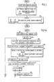
- Figure 2 is a flow diagram which illustrates how the method according to the present invention maximizes balancing among the layers of an interconnection package.
- block 10 depicts the calculation of the CONNTYPE shown on the right side of Table I.
- the first inquiry asks whether the connections of the same net are constrained to lie in the same layer. Taking the simpler case first, i.e., where there is no layer constraint for the nets, the several different CONNTYPES are dealt randomly among all layers. This step is set forth in block 20.. Referring to Table I again, all CONNTYPES (A, D) would be dealt out first. Assuming that there are three layers in the interconnection package, one CONNTYPE (A, D) connection would be assigned to each layer. Similarly, all CONNTYPES are considered in turn. Since there is only one each of CONNTYPES (A, B), (B, C), and (B, D), each in turn would simply be assigned randomly to some layer.
- CONNTYPE A, D
- CONNTYPES B, C and (B, D).
- the assignment of the connections of each CONNTYPE for which the number of connections is not exactly divisible by the number of layers can be made in such a way that the total number of connections (of all CONNTYPES) is the same for all layers, or differs by at most one for the various layers. This is an alternative to dealing the excess connection(s) of each CONNTYPE to layers at random.
- the layer assignments are written. These asssignments will typically be utilized as input to a wire routing process, which may be used to generate art work or control a wiring machine. Upon completion of the steps shown in block 25, the process according to this aspect of the invention is completed.
- each net is initially randomly assigned to one of N layers of the interconnection package.
- the following table illustrates a possible initial random assignment of the nets in three layers.
- the column labeled NET INDEX is similar to the connection index and is simply the row number of the table used for reference purposes.
- the column labeled NETNAME refers to the particular net under consideration each of which is here labeled NET followed by a number.
- the column labeled LAYER simply identifies the layer to which each net has been assigned. In the example shown, NET1 has been assigned to layer 3 while NET2 and NET3 have been assigned to layer 1. No nets have been assigned to layer 2.
- SCORE is a measure of the degree of imbalance of a particular assignment and can be compared to other SCORES. The lower the SCORE value, the more balanced the interconnection package is.
- SCORE is calculated in the following manner. For each CONNTYPE and for each layer from 1 through the last layer, NLAYER, where NL A Y E R represents the total number of layers, the population of that CONNTYPE in a layer is represented as POP (CONNTYPE, LAYER). The population of each CONNTYPE in each layer is counted in block 82. Then an average population of the CONNTYPE per layer, POPAVG (CONNTYPE), is determined by summing the population of each CONNTYPE in all layers and dividing the number of the total number of layers i.e., NLAYER. This may be expressed mathematically as:
- the SCORE is calculated by summing the square of the quantity equal to the difference between the population of each CONNTYPE in each layer and the average population of that CONNTYPE for all layers. The sum is taken over all CONNTYPES and all layers. This is expressed mathematically as:
- CONNTYPE A,D
- the contribution of CONNTYPE (A,D) to the score will be calculated for purposes of illustration: It can readily be seen that if the connections had been distributed evenly among the three layers the SCORE would be equal to zero, indicating perfect balancing of the connections of that CONNTYPE.
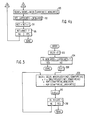
- the next step, shown in block 100 is to reassign nets from the present layer to any other layers to which they may be permissibly assigned. For reasons specific to a particular design, assigning certain nets to one or mere of the other layers may sometimes not be permissible. In cases where some nets are not permitted to be moved, they should be omitted from the NET loop in Figures 4a and 4b. When a net is not permitted to be moved to a particular NEWLAY ER , the WEIGHT for that net and that NEWLAYER should be set equal to zero at block 108. Otherwise, the flow diagrams apply without change.
- Figures 4a and 4b show the details of the REASSIGN subroutine.
- the user specifies some real number for the value T.
- Practice has shown that is useful to start with a value for T which is at least several times larger than the largest value encountered for DELTA, as will be discussed hereinbelow.
- the value of T may be decreased with each loop. If one starts with a value for T that is too low or if one starts high and decreases it too rapidly with each loop, an undesirably large SCORE (i.e., large measure of imbalance) may result.
- the value of NET is simply set equal to 1 so that on subsequent passes through the loop all movable nets will be considered.
- the DELTA value is calculated as will be described hereinbelow in detail in connection with Figure 5.
- the DELTA value is a measure of whether reassigning a net to another layer results in a more balanced interconnection package.
- the expression for DELTA is so chosen that DELTA plus the value of SCORE prior to a reassignment of a net to a new layer, equals the value of SCORE following such reassignment. This is expressed mathematically as:
- the value of DELTA for keeping the net in the same layer, i.e., not reassigning it, is 0.
- the net is not simply assigned to the new layer having the most negative value of DELTA at every step, since by so doing it is found to lead to a final assignment that can be far from optimal.
- a probablility factor or weight is calculated for each DELTA value.
- the weight is mathematically expressed as follows: In other words, the weight represents a number associated with the probability of reassigning a net from one layer, LAYERNET, to a different layer, NEWLAYER, which is an exponential function based on the values of a calculated DELTA and a user specified value'of T.
- a random real number, R is chosen lying between zero and the sum of the weights over all values of NEWLAYER.
- the sum of the previous sum value and the weight is added. If R is not less than or equal to the sum as determined in block 116, the next step is to add 1 to the value of NEWLAYER as shown in block 118. Then, it is necessary to loop back to block 114 to recalculate the sum for the next layer to which the net may be reassigned.
- NEWLAYER may of course happen to equal LAYER(NET). In that case, no layer reassignment occurs.
- L AYER ( NET ) will be set equal to (NEWLAYER) in block 12 2 and the NET index will be increased by 1 in block 124.
- NET is greater than the number of nets, i.e., NNET. If so, then all the nets have been considered. If NET is not greater than NNET then it is necessary to look at the next net and consider the layers, to which it may be reassigned.
- the subroutine of Figure 5 is called once for each net and each value of NEWLAYER.
- the value of DELTA is set to zero in block 202.
- K indexes the rows of a table that is maintained for each net, and is illustrated in Table III for the case of NETl, a net defined in Table I.
- the contribution to the value of DELTA resulting from the Kth entry of this table is calculated in block 208. The contribution is:
- MULTIPLICITY refers to the number of connections of a given CONNTYPE in a given net. Referring to Table I, the MULTIPLICITY of the connections in NET1 is depicted in the following table:
- the K is simply an index value for convenience of reference to the values in the table. It is seen that the MULTIPLICITY for all CONNTYPES in NET1 is one. In principle, one can have multiple connections of the same CONNTYPE for a given net. MULTIPLICITY simply takes account of that possibility.
- the K value is increased by one at block 210. If all K values have been considered, K > LAST and the subroutine is complete. If not, block 208 is re-entered and the contribution of the next row indexed by K is added to DELTA.
- T should be selected such that it is initially at least three or four times the largest value of DELTA.
- T should be reduced, e.g., to 80% or 90% of its value on the preceding pass, and layer reassignment performed for each net.
- a final pass may be performed in which T is set equal to an essentially zero value (e.g., 0.001). This may drive down the value of SCORE even more.
- the value of MAXIMBALANCE provides a direct indication of how imbalanced is the layer assignment of the most imbalanced CONNTYPE.
- MAXIMBALANCE is defined mathematically as:
- the method according to the invention examines each CONNTYPE, in sequence. For each CONNTYPE that is examined, it determines the population of that CONNTYPE in each layer.
- IMBALANCE is defined as the number of connections of that CONNTYPE in the layer containing the largest number of such connections minus the number of connections of that CONNTYPE in the layer containing the smallest number of sucn connections.
- MAXIMBALANCE is the maximum value of IMBALANCE taken over all CONNTYPES. If MAXIMBALANCE is 0 or 1, the layer assignment is as balanced as is possible for the given net list. (Further reassignment cannot possibly reduce a MAXIMBALANCE of 1 to zero.)
- the SCORE and any other diagnostics such as MAXIMBALANCE are written as shown in block 140.
- the user either manually or by coded instruction must determine if the SCORE and/or MAXIMBALANCE values are satisfactory. This is illustrated in block 160. If these values are not satisfactory, it will be necessary to return to block 80 and begin to perform another reassignment pass perhaps with a different value for T, as mentioned above. If the SCORE and/or MAXIMBALANCE values are satisfactory, then the layer assignments are written for all nets is shown in block 18 0. This data typically may be utilized for subsequent wire routing, which will yield detailed path information used to generate artwork or to control physical wiring equipment.
Landscapes
- Engineering & Computer Science (AREA)
- Computer Hardware Design (AREA)
- Physics & Mathematics (AREA)
- Theoretical Computer Science (AREA)
- Computer Networks & Wireless Communication (AREA)
- Evolutionary Computation (AREA)
- Geometry (AREA)
- General Engineering & Computer Science (AREA)
- General Physics & Mathematics (AREA)
- Design And Manufacture Of Integrated Circuits (AREA)
- Complex Calculations (AREA)
- Management, Administration, Business Operations System, And Electronic Commerce (AREA)
Applications Claiming Priority (2)
| Application Number | Priority Date | Filing Date | Title |
|---|---|---|---|
| US06/639,570 US4713773A (en) | 1984-08-10 | 1984-08-10 | Method for distributing wire load in a multilayer package and the resulting product |
| US639570 | 1984-08-10 |
Publications (3)
| Publication Number | Publication Date |
|---|---|
| EP0170971A2 true EP0170971A2 (de) | 1986-02-12 |
| EP0170971A3 EP0170971A3 (en) | 1989-11-08 |
| EP0170971B1 EP0170971B1 (de) | 1993-02-03 |
Family
ID=24564647
Family Applications (1)
| Application Number | Title | Priority Date | Filing Date |
|---|---|---|---|
| EP85109188A Expired - Lifetime EP0170971B1 (de) | 1984-08-10 | 1985-07-23 | Verfahren zur Verteilung der Leitungsbelastung auf einer Schaltkarte oder auf einem Verbindungspackage mit jeweils mehreren Verdrahtungsebenen |
Country Status (4)
| Country | Link |
|---|---|
| US (1) | US4713773A (de) |
| EP (1) | EP0170971B1 (de) |
| JP (1) | JPS6148071A (de) |
| DE (1) | DE3587055T2 (de) |
Families Citing this family (16)
| Publication number | Priority date | Publication date | Assignee | Title |
|---|---|---|---|---|
| DE3650323T2 (de) * | 1986-12-17 | 1996-01-25 | Ibm | VLSI-Chip und Verfahren zur Herstellung. |
| US4831725A (en) * | 1988-06-10 | 1989-05-23 | International Business Machines Corporation | Global wiring by removal of redundant paths |
| US5155692A (en) * | 1989-08-21 | 1992-10-13 | At&T Bell Laboratories | Technique for routing conductive paths |
| US5218551A (en) * | 1990-04-30 | 1993-06-08 | International Business Machines Corporation | Timing driven placement |
| SG68564A1 (en) * | 1994-01-25 | 1999-11-16 | Advantage Logic Inc | Apparatus and method for partitioning resources for interconnections |
| JP3571369B2 (ja) * | 1994-06-16 | 2004-09-29 | 富士通株式会社 | 配線設計装置 |
| US5754826A (en) * | 1995-08-04 | 1998-05-19 | Synopsys, Inc. | CAD and simulation system for targeting IC designs to multiple fabrication processes |
| AU2327997A (en) | 1996-03-15 | 1997-10-01 | University Of Arizona, The | Interconnection routing system |
| US5963728A (en) * | 1996-08-14 | 1999-10-05 | International Business Machines Corporation | Method to partition clock sinks into nets |
| US5920486A (en) * | 1996-08-16 | 1999-07-06 | International Business Machines Corporation | Parameterized cells for generating dense layouts of VLSI circuits |
| US5881789A (en) * | 1997-09-12 | 1999-03-16 | Calapitter Creations, Inc. | Childrens play structure |
| US6189131B1 (en) * | 1998-01-14 | 2001-02-13 | Lsi Logic Corporation | Method of selecting and synthesizing metal interconnect wires in integrated circuits |
| US6182272B1 (en) * | 1998-07-16 | 2001-01-30 | Lsi Logic Corporation | Metal layer assignment |
| US6762489B2 (en) | 2001-11-20 | 2004-07-13 | International Business Machines Corporation | Jogging structure for wiring translation between grids with non-integral pitch ratios in chip carrier modules |
| JP2006005018A (ja) * | 2004-06-15 | 2006-01-05 | Fujitsu Ltd | レイアウト設計装置、レイアウト設計方法、レイアウト設計プログラム、および記録媒体 |
| WO2012147285A1 (ja) * | 2011-04-25 | 2012-11-01 | ルネサスエレクトロニクス株式会社 | 半導体集積回路の配線方法及び配線装置 |
Family Cites Families (5)
| Publication number | Priority date | Publication date | Assignee | Title |
|---|---|---|---|---|
| US3702004A (en) * | 1970-01-08 | 1972-10-31 | Texas Instruments Inc | Process and system for routing interconnections between logic system elements |
| US3653071A (en) * | 1970-01-08 | 1972-03-28 | Texas Instruments Inc | Process for producing circuit artwork utilizing a data processing machine |
| US3681782A (en) * | 1970-12-02 | 1972-08-01 | Honeywell Inf Systems | Machine process for positioning interconnected components to minimize interconnecting line length |
| US3705409A (en) * | 1970-12-09 | 1972-12-05 | Ibm | Tableau network design system |
| US4377849A (en) * | 1980-12-29 | 1983-03-22 | International Business Machines Corporation | Macro assembler process for automated circuit design |
-
1984
- 1984-08-10 US US06/639,570 patent/US4713773A/en not_active Expired - Fee Related
-
1985
- 1985-06-27 JP JP60139268A patent/JPS6148071A/ja active Granted
- 1985-07-23 EP EP85109188A patent/EP0170971B1/de not_active Expired - Lifetime
- 1985-07-23 DE DE8585109188T patent/DE3587055T2/de not_active Expired - Fee Related
Non-Patent Citations (3)
| Title |
|---|
| COMPUTERS & GRAPHICS, vol. 7, no. 3/4, 1983, pages 333-347, Pergamon Press Ltd, Exeter, GB; L.M. PATNAIK et al.: "Implementation of placement and routing algorithms for computer aided design of printed circuit boards" * |
| IEEE TRANS. ON COMPUTER AIDED DESIGN, vol. CAD-2, No. 4, Oct. 1983, pages 215-222, M. P. Vecchi and S. Kirkpatrick: " Global wiring by simulated an-nealing". * |
| IEEE TRANSACTIONS ON CIRCUITS AND SYSTEMS, vol. CAS-31, no. 5, May 1984, pages 462-472, IEEE, New York, US; R. RAGHAVAN et al.: "The complexity of single row routing" * |
Also Published As
| Publication number | Publication date |
|---|---|
| EP0170971A3 (en) | 1989-11-08 |
| EP0170971B1 (de) | 1993-02-03 |
| JPH0587867B2 (de) | 1993-12-20 |
| DE3587055D1 (de) | 1993-03-18 |
| US4713773A (en) | 1987-12-15 |
| JPS6148071A (ja) | 1986-03-08 |
| DE3587055T2 (de) | 1993-08-12 |
Similar Documents
| Publication | Publication Date | Title |
|---|---|---|
| EP0170971B1 (de) | Verfahren zur Verteilung der Leitungsbelastung auf einer Schaltkarte oder auf einem Verbindungspackage mit jeweils mehreren Verdrahtungsebenen | |
| US4500963A (en) | Automatic layout program for hybrid microcircuits (HYPAR) | |
| US6353918B1 (en) | Interconnection routing system | |
| EP0143366B1 (de) | Verfahren zur Platzierung von Elementen | |
| US5657242A (en) | Method of determining routes for a plurality of wiring connections and a circuit board produced by such a method | |
| US4815003A (en) | Structured design method for high density standard cell and macrocell layout of VLSI chips | |
| EP0133466B1 (de) | Gleichzeitige Plazierung und Verbindung von VLSI-Chips | |
| US4615011A (en) | Iterative method for establishing connections and resulting product | |
| US5404313A (en) | System for assigning positions of block terminals in a VLSI | |
| US5898597A (en) | Integrated circuit floor plan optimization system | |
| US5636129A (en) | Electrical routing through fixed sized module and variable sized channel grids | |
| US20010038612A1 (en) | Automatic routing system for circuit layout | |
| JPH077427B2 (ja) | ノードの相互接続方法 | |
| Abel | On the ordering of connections for automatic wire routing | |
| WO1997034316A9 (en) | Interconnection routing system | |
| Suaris et al. | A quadrisection-based combined place and route scheme for standard cells | |
| JP2004287681A (ja) | 配線設計支援システム、および、配線設計支援方法 | |
| JP2001015637A (ja) | 回路配線方式及び回路配線方法及び半導体パッケージ及び半導体パッケージ基板 | |
| EP0163978B1 (de) | Verfahren zum Bezeichnen elektrischer Verbindungen auf einem integrierten Produkt und das resultierende Produkt | |
| JPH0669067B2 (ja) | ベイ・パッキング方法 | |
| US5701255A (en) | Cell generation method and cell generation system | |
| US5734583A (en) | Capacitance forming method | |
| US6532580B1 (en) | In-place method for inserting repeater buffers in an integrated circuit | |
| US7428719B2 (en) | Layout of network using parallel and series elements | |
| US5475611A (en) | Circuit structure, semiconductor integrated circuit and path routing method and apparatus therefor |
Legal Events
| Date | Code | Title | Description |
|---|---|---|---|
| PUAI | Public reference made under article 153(3) epc to a published international application that has entered the european phase |
Free format text: ORIGINAL CODE: 0009012 |
|
| AK | Designated contracting states |
Designated state(s): DE FR GB |
|
| 17P | Request for examination filed |
Effective date: 19860624 |
|
| PUAL | Search report despatched |
Free format text: ORIGINAL CODE: 0009013 |
|
| AK | Designated contracting states |
Kind code of ref document: A3 Designated state(s): DE FR GB |
|
| 17Q | First examination report despatched |
Effective date: 19911127 |
|
| GRAA | (expected) grant |
Free format text: ORIGINAL CODE: 0009210 |
|
| AK | Designated contracting states |
Kind code of ref document: B1 Designated state(s): DE FR GB |
|
| REF | Corresponds to: |
Ref document number: 3587055 Country of ref document: DE Date of ref document: 19930318 |
|
| ET | Fr: translation filed | ||
| PLBE | No opposition filed within time limit |
Free format text: ORIGINAL CODE: 0009261 |
|
| STAA | Information on the status of an ep patent application or granted ep patent |
Free format text: STATUS: NO OPPOSITION FILED WITHIN TIME LIMIT |
|
| 26N | No opposition filed | ||
| PGFP | Annual fee paid to national office [announced via postgrant information from national office to epo] |
Ref country code: FR Payment date: 19950704 Year of fee payment: 11 |
|
| PGFP | Annual fee paid to national office [announced via postgrant information from national office to epo] |
Ref country code: DE Payment date: 19950720 Year of fee payment: 11 |
|
| PGFP | Annual fee paid to national office [announced via postgrant information from national office to epo] |
Ref country code: GB Payment date: 19960621 Year of fee payment: 12 |
|
| PG25 | Lapsed in a contracting state [announced via postgrant information from national office to epo] |
Ref country code: FR Effective date: 19970328 |
|
| PG25 | Lapsed in a contracting state [announced via postgrant information from national office to epo] |
Ref country code: DE Effective date: 19970402 |
|
| REG | Reference to a national code |
Ref country code: FR Ref legal event code: ST |
|
| PG25 | Lapsed in a contracting state [announced via postgrant information from national office to epo] |
Ref country code: GB Free format text: LAPSE BECAUSE OF NON-PAYMENT OF DUE FEES Effective date: 19970723 |
|
| GBPC | Gb: european patent ceased through non-payment of renewal fee |
Effective date: 19970723 |