EP0168280A1 - Anordnung zum Abtasten von optisch-magnetischen Zeichen mit Druck- und Speichermöglichkeit - Google Patents
Anordnung zum Abtasten von optisch-magnetischen Zeichen mit Druck- und Speichermöglichkeit Download PDFInfo
- Publication number
- EP0168280A1 EP0168280A1 EP85401082A EP85401082A EP0168280A1 EP 0168280 A1 EP0168280 A1 EP 0168280A1 EP 85401082 A EP85401082 A EP 85401082A EP 85401082 A EP85401082 A EP 85401082A EP 0168280 A1 EP0168280 A1 EP 0168280A1
- Authority
- EP
- European Patent Office
- Prior art keywords
- output
- comparator
- characters
- check
- reading
- Prior art date
- Legal status (The legal status is an assumption and is not a legal conclusion. Google has not performed a legal analysis and makes no representation as to the accuracy of the status listed.)
- Granted
Links
Images


Classifications
-
- G—PHYSICS
- G06—COMPUTING OR CALCULATING; COUNTING
- G06K—GRAPHICAL DATA READING; PRESENTATION OF DATA; RECORD CARRIERS; HANDLING RECORD CARRIERS
- G06K7/00—Methods or arrangements for sensing record carriers, e.g. for reading patterns
- G06K7/08—Methods or arrangements for sensing record carriers, e.g. for reading patterns by means detecting the change of an electrostatic or magnetic field, e.g. by detecting change of capacitance between electrodes
- G06K7/082—Methods or arrangements for sensing record carriers, e.g. for reading patterns by means detecting the change of an electrostatic or magnetic field, e.g. by detecting change of capacitance between electrodes using inductive or magnetic sensors
- G06K7/083—Methods or arrangements for sensing record carriers, e.g. for reading patterns by means detecting the change of an electrostatic or magnetic field, e.g. by detecting change of capacitance between electrodes using inductive or magnetic sensors inductive
- G06K7/084—Methods or arrangements for sensing record carriers, e.g. for reading patterns by means detecting the change of an electrostatic or magnetic field, e.g. by detecting change of capacitance between electrodes using inductive or magnetic sensors inductive sensing magnetic material by relative movement detecting flux changes without altering its magnetised state
-
- G—PHYSICS
- G06—COMPUTING OR CALCULATING; COUNTING
- G06K—GRAPHICAL DATA READING; PRESENTATION OF DATA; RECORD CARRIERS; HANDLING RECORD CARRIERS
- G06K13/00—Conveying record carriers from one station to another, e.g. from stack to punching mechanism
- G06K13/02—Conveying record carriers from one station to another, e.g. from stack to punching mechanism the record carrier having longitudinal dimension comparable with transverse dimension, e.g. punched card
- G06K13/07—Transporting of cards between stations
-
- G—PHYSICS
- G06—COMPUTING OR CALCULATING; COUNTING
- G06K—GRAPHICAL DATA READING; PRESENTATION OF DATA; RECORD CARRIERS; HANDLING RECORD CARRIERS
- G06K17/00—Methods or arrangements for effecting co-operative working between equipments covered by two or more of main groups G06K1/00 - G06K15/00, e.g. automatic card files incorporating conveying and reading operations
Definitions
- the invention relates to devices of the family known as "point of sale terminals", intended to at least partially automate commercial and financial transactions.
- terminals are intended to be installed for example at a merchant, who executes a transaction with his client, who most of the time provides a check as a means of payment.
- terminals of this kind which are suitable for collection - financial transaction - following a commercial transaction.
- terminals capable of printing the amount of the transaction on the check, which the customer therefore only has to sign.
- Such a solution remains imperfect, because the merchant still has to acquire or "enter” the characteristics of the check for his accounting.
- the bank processing of checks (clearing house in particular) is an expensive operation, which should therefore be simplified as much as possible.
- the main object of the present invention is to provide a solution to these problems.
- a device for reading the magnetic- optical characters of checks such as the so-called CMC7 characters, or alternatively those called E13B, comprising a track suitable for receiving and driving a document such a check carrying these characters, in a predetermined position, a means or head for pre-magnetizing the characters, a character reading transducer, and electronic control and processing means connected to this transducer.
- Reading magnetic-optical characters is a fairly delicate operation, for which it has hitherto been considered that the heads or transducers should be in a fixed position relative to the document to be read.
- the present invention recommends that the track comprises, for receiving the document, rollers of fixed axis relative to a frame of the device, while the transducers themselves are mounted floating, respectively opposite these rollers, and urged elastically towards these on command.
- each transducer is mounted at the end of an arm of a respective L-shaped lever, pivotally articulated at its angle on the frame, while the two levers are biased, at the end of their other arm, by means of respective elastic means, by an actuating rod controlled by an electromagnet.
- the rod is itself subjected to an elastic return, against its stress by the electromagnet.
- the aforementioned reading device is supplemented by electronic means specific to the execution of a commercial transaction, as well as by printing means and logic control means.
- These logical control means are arranged to provide, after the execution of a commercial transaction, validated by the two parties, a series of commands specific to reading the optical-magnetic characters of a check, and printing on this check for the amount of the transaction.
- the logical ordering means also produce the impression of a customer ticket, and of a merchant's journal. It is possible, on this journal, printed continuously on a tape, to report the characteristics read on the check. This can be replaced or supplemented by the complete recording of the characteristics of the transaction in an electronic memory specific to the merchant.
- the logic control means are further capable of presenting jointly, to a local memory, or to a remote memory, electrical signals which jointly represent characters read from the check, and characteristics of the transaction, which allows; simplification of the bank processing of checks.
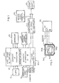
- the DILC device is suitable for printing a customer ticket TCL, as well as a merchant journal JCO, which can be in the form of a continuous strip.
- a blank check can be entered into the DILC system, which returns it, coated with the amount of the transaction to the client, for signature.
- all of the devices which are under the control of the logic control unit ULC allow the supply of electrical signals representative of the characteristics of the check and of the transaction to a CCT unit, which ensures their recording on a local memory ML, such as a floppy disk, and / or transmission to a remote memory MD, for example by the telephone network.
- a CCT unit which ensures their recording on a local memory ML, such as a floppy disk, and / or transmission to a remote memory MD, for example by the telephone network.
- FIG 2 is a general view of the DILC device.
- the DI printing device itself, which may be of known structure, has a head printing placed in IT, for example a printhead. needle (not shown in detail), equipped with a ' CP backplate, while we see in GR a return roller intended to ensure the movement of the print head.
- the set of movements required for the DILC device can be provided by an MPP1 stepper motor.
- a first roller (not visible) provides a strip of paper on which the printing head TI can draw up the customer's ticket, which is finally cut by a cutter M under the control of an electromagnet EM1.
- a second roller continuously delivers another strip of paper, which is present on the counterplate CP adjacent to the first, and on which the print head will be able to establish the merchant's journal.
- the check actuates a drive mechanism from another stepping motor MPP2, which solicits rollers G1 and G2 which will make pass the check at a controlled speed in parts T2 then T3 of its route.
- the front edge of the check will be detected by the D02 detector, which allows the UCL central unit to define a validation signal for reading CMC7 characters.
- this reading is done by a head TM2 placed opposite the roller G2, while a head TM1 placed opposite the roller G1 has previously premagnetized the inscriptions CMC7 of the check (FIGS. 2 to 4).
- the check goes back up to be in the printing operating position on the CP backplate.
- Printing on the check is then ordered.
- This print includes the inscription (in clear) of the amount of the transaction, the place, the date and the beneficiary.
- This im pressure is carried out column by column, since the print head moves perpendicular to the normal direction of writing on a check. This also makes it possible to generate characters in a different font than that of conventional needle printers (double vertical format for example). The risks of fraud are then much reduced.
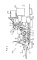
- FIGS. 3 and 4 Reference is now made specifically to FIGS. 3 and 4, for a more detailed description of the reading of the magnetic characters of the check.
- the premagnetization head TM1 This head is supported at the end L11 of a lever in the general shape of L, noted as a whole L1. At its angle L10, the lever is pivotally articulated by an axis L13 on the frame BM. The other arm, L12, of the lever, descends downwards, where it offers a stud L14, which engages in a first eyelet AC11, oblong, formed in an actuating rod AC. On this stud L14 is hooked a spring L15, which also bears on the rod AC itself.
- the head TM1 In the rest position, the head TM1 is at a distance from the roller G1.
- an electromagnet EM2 When an electromagnet EM2 is actuated by the UCL unit, its plunger core pulls the AC rod on which it is articulated, which results in a displacement of the AC rod to the right, and consequently from the eyelet AC11 of that: ci around the nipple L14.
- the nipple is at the same time urged elastically to the right, which lowers the head TM1 towards the roller G1.
- the fulcrum of the spring L15 on the rod AC is therefore to the right of the eyelet AC11 housing the stud L14.
- a spring AC10 there is provided on the left, at the free end of the rod AC, a spring AC10 for the return of the latter relative to the frame, in order to return the heads to their normal rest position.
- a lever L2 articulated at its angle L20 on the frame carries at the end of one of its arms L21 the head of TM2 reading, while its other end L22 carries a pin L24 movable in the eyelet AC12, and capable of being pulled to the right by a spring L25.
- the check is driven by the fact that the lower rollers G1 and / or G2 are driven from the aforementioned stepping motor, or an equivalent motor means.
- the rollers G1 and G2 are of course coated with a suitable material, which is for example 40 Shore A hardness neoprene sold by Dupont de Nemours.
- FIG. 4 is a top view corresponding to a section along the broken line AA of FIG. 3. It shows a check formula, at the start of its introduction on the plate T1. Unlike Figure 3, it also shows the optical detectors D01 and D02.
- the magnetic heads TM1 and TM2 there are provided counter-rollers G11 and G12, located opposite the rollers G1 and G2, and which can be provided with the same coating. peripheral than these.
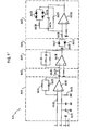
- FIG. 5 schematically illustrates the magnetic head TM2, connected to an electronic card for reading DLC characters.
- the TM2 magnetic head has a TM20 shield inside which a TM21 magnetic circuit is placed. On this magnetic circuit are provided two windings TM22 and TM23, with a common point.
- the air gap of the magnetic circuit TM21 is of the order of 40 microns, in a known manner. It has been found that such an armored read head can be obtained from the UK Company Magnetic Components Ltd. allows a better reading of the CMC7 characters carried on the check.
- FIG. 6, illustrates the overall composition of the device for reading the DLC characters of FIG. 5.
- the DLC device While the control logic unit normally operates at a voltage of 5 volts, the DLC device operates at two voltages of plus and minus 12 volts, which are first subjected to filtering in a FAL circuit. From these voltages, an APM device supplies the premagnetization head TM1. As a variant, this premagnetization head can be replaced by a head with a permanent magnet.
- the four aforementioned connections, emanating from the TM2 read head (in particular Figure 5) are applied to an anti-saturation analog amplification chain, noted as a whole AA.
- This amplification chain provides analog electrical signals, representative of the function. tion of transducer produced by the TM2 head.
- FIG. 7 illustrates the detailed structure of the AA amplification chain.
- the two hot spots coming from the windings TM22 and TM23 are noted 1 and 2 respectively. They are applied to a low noise preamplifier noted: AA1.
- This consists of an AA10 differential amplifier, such as the ADOP07 model sold by the United States Company Analog Devices. Signals 1 and 2 are applied to the inverting input and the non-inverting input of this AA10 amplifier respectively.
- Each link thus formed comprises in parallel on the ground a capacitor of 220 picofarads for example, and in series a resistance of 3300 kilo-ohms, such as AA11 and AA12.
- the non-inverting input is connected to ground by an AA13 resistor of 390 kilo-ohms (all numerical values given by way of example).
- the inverting input of the amplifier AA10 is connected to its output by the parallel network of a resistance AA14 equal to the resistance AA13, and of a capacitor AA15 of approximately 100 picofarads.
- This low noise preamplifier is followed by a connection specific to the elimination of the humming noise linked to the sector (50 Hertz in France).
- a capacitor AA20 1 of 22 nanofarads is followed by a resistance AA21 of 3300 ohms, which is in turn connected to the inverting input of a subsequent amplifier AA30, forming part of an amplifier stage AA3.
- the non-inverting input of this AA30 amplifier which is for example the LM358 model from the Motorola Company, is connected to ground by another 3300 ohm resistor.
- the output of the amplifier AA30 is connected to a link intended to form a noise suppression.
- the part AA4 of the means AA begins with a capacitor AA40, of a value of 1 microfarad for example, and followed by two diodes AA41 and AA42, mounted head to tail in parallel. These two diodes are silicon diodes such as the 1N4148 model, having a threshold voltage of 0.2 to 0.3 volts.
- the output of this section AA4 of the assembly is then applied to the last stage AA5, which is the amplifier stage with "logarithmic" gain, or more precisely with non-linear anti-saturation gain characteristic.
- the link is provided by a 33 kilo-ohm AA51 resistor up to the inverting input of the AA50 amplifier. This is again the LM358 model for example. Its non-inverting input is connected to ground by another resistor of the same value as the resistor AA51.
- the feedback network mounted between the output and the inverting input of the amplifier AA50 comprises a channel provided with an AA53 resistance, of 330 kilo-ohms for example, a parallel channel provided with a capacity of 100 picofarads noted AA54, and a third parallel channel made up of two pairs of diodes, in parallel one on the other.
- the AA55 pair consists of two 1N4148 diodes connected in series in the same direction.
- the pair AA56 consists of two diodes connected in series, in opposite directions. This double pair of diodes in parallel is mounted on a resistance AA58 which measures for example 82 kilo-ohms.
- the logarithmic or anti-saturation characteristic of this stage AA5 is essentially provided by the two pairs of diodes AA55 and AA56.
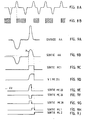
- FIGS. 8A to 8B The second schematically illustrates portions of CMC7 characters (truncated at the top and bottom). Opposite, FIG. 8A illustrates the magnetic transitions read by the head TM2 (theoretical signal purified of any noise).
- FIG. 9A illustrates a signal likely to appear at the input of the amplification chain, comprising various types of alterations which produce one of the noise around zero, the other differences in the form of a negative signal and a positive signal adjacent to each other.
- FIG. 9B shows how a signal will be obtained at the output of the amplification chain AA which is first of all devoid of any noise, due on the one hand to the link AA2 which filters the sector noises, and on the other hand part of the AA4 link which filters noises close to zero, or more exactly the DC component defined by the capacitor AA40.
- the stage AA5 by its logarithmic or anti-saturation characteristic tends to reduce the amplitude differences existing between the successive signals, here a negative signal and a positive signal, given by way of example, it being observed that the negative signals will not be used in. the following.
- the AA5 circuit avoids sudden clipping of high amplitude signals, which would hinder the determination of their peak, which is necessary as will be seen below.
- the comparator MC1 assembly includes a comparative amplifier . rator MC10, whose non-inverting input receives the output of the AA circuit. Its inverting input is connected to a voltage divider normally supplying a voltage of 0.46 volts, by a resistive voltage divider MC11, MC12 mounted between the voltage of +12 volts and ground. The output of comparator MC10 is connected to the voltage +12 volts by a resistor MC13. It is also connected to an inverting amplifier MC14, the output of which meets the cathode of a diode MC15, the anode of which is connected to the inverting input of the amplifier MC10.
- the comparator output signal illustrated in FIG. 9C can therefore only return to zero (logic) when the half-wave P drops below about 0.1 volts. This results in a hysteresis on the operation of the comparator assembly MC1.
- the comparator MC10 is for example the LM319 model from the National Semiconductor Company.
- the comparator assembly MC2 essentially comprises a fast comparator amplifier MC20, such as the model TDB0353DP sold by the French company Thomson CSF.
- the non-inverting input of this comparator MC20 is connected to the output of the amplification chain AA. Its output is connected to the anode of a diode (1N4148) denoted MC25, and whose cathode joins the inverting input of the same amplifier.
- This input is further connected by an MC24 resistor, of 1000 ohms for example, to a capacitor MC23, whose capa-. cited is for example 22 nanofarads.
- the capacitor MC23 ' is also connected to ground. Its common point with the resistor MC24 is connected to the anode of a Schottky diode MC22, the cathode of which joins a resistor MC21, in turn connected to the output of the comparator MC10.
- the output of the comparator MC10 is low, and the diode MC22 thus prevents the capacitor MC23 from charging above 0.1 volts.
- the in! The MC20 comparator's inverting input therefore receives this voltage as a reference, and its non-inverting input in principle receives a lower voltage during the same period, from which it follows that the output of the MC20 comparator is close to - 12 volts. The MC25 diode is therefore blocked.
- the capacitor MC23 can charge. It will do this as soon as the voltage present on the non-inverting input of the comparator MC20 rises, as illustrated in FIG. 9D, and this throughout the beginning of the alternation P of the output signal of the chain AA. Once the peak of this alternation P has been reached, the charge of the capacitor is maintained until the output of the comparator MC10 drops to its low level.
- the output of the comparator MC20 rises during the charging of the capacitor MC23, that is to say during the rising part of the signal P of FIG. 9B. It thus goes up to around 12 volts. But as soon as the alternation P goes down again, the output of the comparator MC20 suddenly drops to zero, thus producing a useful transition logic signals.
- this output is applied to the inverting input of a comparator MC26, such as the LM319 model already mentioned, and whose non-inverting input receives a reference voltage of -6 volts.
- a comparator MC26 such as the LM319 model already mentioned
- An inverting amplifier MC28 then supplies a signal as illustrated in FIG. 9G, to be applied to the second input of the NAND gate ML10, the first input of which receives the output of the comparator MC10.
- the output of this same gate is applied to the clock input of a flip-flop ML1, of the memory flip-flop type.
- Input D thereof receives a +12 volt signal. Its reset input R receives the output of the inverter MC14.
- the flip-flop is therefore forced to zero as long as the comparator MC10 has its output at a low level. While this same output is at the high level, the signal supplied by the NAND gate ML10 in response to the comparator assembly MC2 allows a change of state of the flip-flop ML1. This returns to zero as soon as the output of the comparator assembly MC1 returns to zero.
- the logic means ML comprise a second flip-flop, the clock input of which is connected to the output Q of the first flip-flop ML1.
- This flip-flop is mounted as a flip-flop, by the fact that its inverted output Q is connected to its storage input D.
- the validation input S of the flip-flop ML2 is subject to a read authorization from a microprocessor of the UCL unit, from an ML20 adaptation circuit to go from a voltage of 5 volts to a voltage of 12 volts.
- the circuit which has just been described has many significant advantages, including the fact that the first comparator assembly MC1 avoids the taking into account of bounces of the incident signal, around the zero value, thus defining a kind of reading window.
- the second comparator assembly MC2 which is in principle sensitive to any passage above zero of the incident signal, can only operate when said window is open. Conversely, when said window is open, it is only possible to take into consideration one and only one transition provided by the comparator assembly MC2, it being observed that several transitions could occur in the case of the aforementioned rebounds.
- these characteristics of the check are transmitted by an online transmission to a remote memory, which can be located in the bank with which the merchant usually works.
Landscapes
- Engineering & Computer Science (AREA)
- Physics & Mathematics (AREA)
- General Physics & Mathematics (AREA)
- Theoretical Computer Science (AREA)
- Artificial Intelligence (AREA)
- Computer Vision & Pattern Recognition (AREA)
- Character Input (AREA)
- Credit Cards Or The Like (AREA)
- Printers Or Recording Devices Using Electromagnetic And Radiation Means (AREA)
- Printers Characterized By Their Purpose (AREA)
- Financial Or Insurance-Related Operations Such As Payment And Settlement (AREA)
Priority Applications (1)
| Application Number | Priority Date | Filing Date | Title |
|---|---|---|---|
| AT85401082T ATE58604T1 (de) | 1984-06-08 | 1985-05-31 | Anordnung zum abtasten von optisch-magnetischen zeichen mit druck- und speichermoeglichkeit. |
Applications Claiming Priority (2)
| Application Number | Priority Date | Filing Date | Title |
|---|---|---|---|
| FR8409082A FR2565715B1 (fr) | 1984-06-08 | 1984-06-08 | Dispositif de lecture de caracteres magnetiques-optiques avec possibilite d'impression et de memorisation |
| FR8409082 | 1984-06-08 |
Publications (2)
| Publication Number | Publication Date |
|---|---|
| EP0168280A1 true EP0168280A1 (de) | 1986-01-15 |
| EP0168280B1 EP0168280B1 (de) | 1990-11-22 |
Family
ID=9304872
Family Applications (1)
| Application Number | Title | Priority Date | Filing Date |
|---|---|---|---|
| EP85401082A Expired - Lifetime EP0168280B1 (de) | 1984-06-08 | 1985-05-31 | Anordnung zum Abtasten von optisch-magnetischen Zeichen mit Druck- und Speichermöglichkeit |
Country Status (5)
| Country | Link |
|---|---|
| US (1) | US4748673A (de) |
| EP (1) | EP0168280B1 (de) |
| AT (1) | ATE58604T1 (de) |
| DE (1) | DE3580623D1 (de) |
| FR (1) | FR2565715B1 (de) |
Cited By (2)
| Publication number | Priority date | Publication date | Assignee | Title |
|---|---|---|---|---|
| EP0507290A3 (en) * | 1991-04-05 | 1993-05-05 | Mantegazza Antonio Arti Grafiche S.R.L. | Device for detecting coding regions particularly for reading forms in general |
| EP0640841A1 (de) * | 1993-08-31 | 1995-03-01 | Eastman Kodak Company | Vorrichtung und Verfahren zur Banknotenauthentifizierung |
Families Citing this family (16)
| Publication number | Priority date | Publication date | Assignee | Title |
|---|---|---|---|---|
| US5201010A (en) * | 1989-05-01 | 1993-04-06 | Credit Verification Corporation | Method and system for building a database and performing marketing based upon prior shopping history |
| US5305196A (en) | 1989-05-01 | 1994-04-19 | Credit Verification Corporation | Check transaction processing, database building and marketing method and system utilizing automatic check reading |
| US5237620A (en) * | 1989-05-01 | 1993-08-17 | Credit Verification Corporation | Check reader method and system for reading check MICR code |
| US5649114A (en) | 1989-05-01 | 1997-07-15 | Credit Verification Corporation | Method and system for selective incentive point-of-sale marketing in response to customer shopping histories |
| US8700458B2 (en) | 1989-05-01 | 2014-04-15 | Catalina Marketing Corporation | System, method, and database for processing transactions |
| US5621812A (en) | 1989-05-01 | 1997-04-15 | Credit Verification Corporation | Method and system for building a database for use with selective incentive marketing in response to customer shopping histories |
| US5644723A (en) * | 1989-05-01 | 1997-07-01 | Credit Verification Corporation | Method and system for selective incentive point-of-sale marketing in response to customer shopping histories |
| US5198975A (en) * | 1989-11-30 | 1993-03-30 | Valley National Bank | Apparatus and method for processing of check batches in banking operations |
| US6292786B1 (en) | 1992-05-19 | 2001-09-18 | Incentech, Inc. | Method and system for generating incentives based on substantially real-time product purchase information |
| US5925866A (en) * | 1997-09-16 | 1999-07-20 | International Business Machines Corporation | Method, apparatus and article of manufacture for dynamically positioning magnetic shielding to reduce magnetic interference at a magnetic read head |
| US6279827B1 (en) | 1999-04-29 | 2001-08-28 | International Business Machines Corporation | Method, apparatus and article of manufacture for dynamically positioning magnetic shielding to reduce magnetic interference at a magnetic read head |
| US6609104B1 (en) | 1999-05-26 | 2003-08-19 | Incentech, Inc. | Method and system for accumulating marginal discounts and applying an associated incentive |
| US6993498B1 (en) | 1999-07-15 | 2006-01-31 | Midnight Blue Remote Access, Llc | Point-of-sale server and method |
| US7720313B2 (en) * | 2005-12-16 | 2010-05-18 | Ncr Corporation | Digitized bank checks validated by digital signatures |
| KR101871945B1 (ko) * | 2013-01-17 | 2018-08-02 | 한화에어로스페이스 주식회사 | 영상 처리 장치 및 방법 |
| GB2597443A (en) * | 2020-07-21 | 2022-02-02 | Macon Man And Design Ltd | A magnetic pattern recognition sensor |
Citations (6)
| Publication number | Priority date | Publication date | Assignee | Title |
|---|---|---|---|---|
| US4023203A (en) * | 1974-12-04 | 1977-05-10 | Fujitsu Ltd. | System for compensating a phase difference between magnetic tracks in a magnetic recorded information regenerating apparatus |
| US4040108A (en) * | 1974-07-31 | 1977-08-02 | Kabushiki Kaisha Sankyo Seiki Seisakusho | Magnetic sheet reader |
| DE2709379A1 (de) * | 1977-03-01 | 1978-09-07 | Wolfgang Dipl Ing Suhrmann | Einrichtung zur bearbeitung von belegen |
| US4345168A (en) * | 1977-02-25 | 1982-08-17 | Fisher Alan J | Electrical peak detector |
| FR2515390A1 (fr) * | 1980-10-03 | 1983-04-29 | Bradesco Fundacao | Dispositif de lecteur lineaire a commande manuelle pour la lecture de caracteres cmc-7 imprimes sur des documents |
| GB2114346A (en) * | 1982-01-29 | 1983-08-17 | Tokyo Shibaura Electric Co | Apparatus for issuing bond, ticket, certificate or the like |
Family Cites Families (5)
| Publication number | Priority date | Publication date | Assignee | Title |
|---|---|---|---|---|
| US3949363A (en) * | 1974-06-28 | 1976-04-06 | Recognition Equipment, Incorporated | Bar-Code/MICR/OCR merge |
| FR2441222A1 (fr) * | 1978-08-10 | 1980-06-06 | Labin Edouard | Systeme de reglements par cheques permettant leur validation instantanee en tous lieux |
| US4331863A (en) * | 1980-10-29 | 1982-05-25 | Service Distributors, Inc. | Punch mechanism for machine actuator cards |
| US4404649A (en) * | 1980-11-03 | 1983-09-13 | Recognition Equipment Incorporated | Document processing system |
| US4385285A (en) * | 1981-04-02 | 1983-05-24 | Ncr Corporation | Check dispensing terminal |
-
1984
- 1984-06-08 FR FR8409082A patent/FR2565715B1/fr not_active Expired
-
1985
- 1985-05-31 DE DE8585401082T patent/DE3580623D1/de not_active Expired - Lifetime
- 1985-05-31 EP EP85401082A patent/EP0168280B1/de not_active Expired - Lifetime
- 1985-05-31 AT AT85401082T patent/ATE58604T1/de not_active IP Right Cessation
- 1985-06-04 US US06/740,966 patent/US4748673A/en not_active Expired - Fee Related
Patent Citations (6)
| Publication number | Priority date | Publication date | Assignee | Title |
|---|---|---|---|---|
| US4040108A (en) * | 1974-07-31 | 1977-08-02 | Kabushiki Kaisha Sankyo Seiki Seisakusho | Magnetic sheet reader |
| US4023203A (en) * | 1974-12-04 | 1977-05-10 | Fujitsu Ltd. | System for compensating a phase difference between magnetic tracks in a magnetic recorded information regenerating apparatus |
| US4345168A (en) * | 1977-02-25 | 1982-08-17 | Fisher Alan J | Electrical peak detector |
| DE2709379A1 (de) * | 1977-03-01 | 1978-09-07 | Wolfgang Dipl Ing Suhrmann | Einrichtung zur bearbeitung von belegen |
| FR2515390A1 (fr) * | 1980-10-03 | 1983-04-29 | Bradesco Fundacao | Dispositif de lecteur lineaire a commande manuelle pour la lecture de caracteres cmc-7 imprimes sur des documents |
| GB2114346A (en) * | 1982-01-29 | 1983-08-17 | Tokyo Shibaura Electric Co | Apparatus for issuing bond, ticket, certificate or the like |
Non-Patent Citations (1)
| Title |
|---|
| HEWLETT-PACKARD JOURNAL, volume 34, no. 6, juin 1983, pages 15-23, Amstelveen, NL; K.R. HOECKER et al.: "Handpulled magnetic card, mass storage system for a portable computer" * |
Cited By (2)
| Publication number | Priority date | Publication date | Assignee | Title |
|---|---|---|---|---|
| EP0507290A3 (en) * | 1991-04-05 | 1993-05-05 | Mantegazza Antonio Arti Grafiche S.R.L. | Device for detecting coding regions particularly for reading forms in general |
| EP0640841A1 (de) * | 1993-08-31 | 1995-03-01 | Eastman Kodak Company | Vorrichtung und Verfahren zur Banknotenauthentifizierung |
Also Published As
| Publication number | Publication date |
|---|---|
| US4748673A (en) | 1988-05-31 |
| EP0168280B1 (de) | 1990-11-22 |
| FR2565715B1 (fr) | 1987-09-04 |
| ATE58604T1 (de) | 1990-12-15 |
| DE3580623D1 (de) | 1991-01-03 |
| FR2565715A1 (fr) | 1985-12-13 |
Similar Documents
| Publication | Publication Date | Title |
|---|---|---|
| EP0168280B1 (de) | Anordnung zum Abtasten von optisch-magnetischen Zeichen mit Druck- und Speichermöglichkeit | |
| EP0589755B1 (de) | Spielterminal | |
| US6119932A (en) | Identification verification apparatus and method | |
| EP0995161B1 (de) | Kassiervorrichtung, -verfahren und -rechnersystem zur automatischen ausgabe von kommerziellen rabattmarken | |
| EP0172765A1 (de) | Auf dem Merkmal einer Oberflächenstruktur beruhendes Zugangskontrollverfahren und- system | |
| FR2673741A1 (fr) | Circuit de reproduction numerique pour une carte magnetique, notamment pour ticket de route a peage. | |
| US4024379A (en) | Binary system for magnetic card actuation for laundry machines | |
| FR2765014A1 (fr) | Procede d'authentification d'un document en papier, document de securite en papier, et dispositif de controle de l'authenticite de documents en papier | |
| CH680409B5 (de) | ||
| FR2625343A1 (fr) | Perfectionnements aux dispositifs de traitement du signal | |
| EP0297014A1 (de) | Verfahren zur gleichzeitigen Überprüfung der Echtheit eines Datenträgers und der Nichtfälschung seiner Daten und Vorrichtung zum Durchführen dieses Verfahrens | |
| EP0010495B1 (de) | Vorrichtung zur Fehlerverbesserung in einem Erkennungssystem für kodierte Zeichen | |
| FR2640062A1 (fr) | Procede de tarification et dispositif en faisant application | |
| FR2508678A2 (fr) | Procede et dispositif integre de saisie, de traitement et de controle sur le lieu d'une transaction de tous titres de paiement tels que cheques, cartes magnetiques et cartes a memoire | |
| FR2625578A1 (fr) | Systeme de controle de paiement par cartes magnetiques | |
| EP0082175A1 (de) | Verfahren und integrierte einrichtung zur erfassung, verarbeitung und prüfung von zahlungsmitteln, wie schecks, magnetkarten und speicherkarten mittels eines transaktionsterminals | |
| EP1695302B1 (de) | Bezahlungsempfangseinrichtung und verfahren mit identifikationsbild-erfassung | |
| EP0349360B1 (de) | Verfahren zur magnetischen Charakterisierung der Registrierungsschicht eines magnetischen Informationsträgers | |
| JPS6124199B2 (de) | ||
| FR2583550A1 (fr) | Procede et dispositif d'elimination de cartes de credit magnetiques rejetees | |
| KR940004533Y1 (ko) | 자기 카드의 위조 감식장치 및 자기기록 매체 | |
| FR2576439A1 (fr) | Systeme securise d'impression a distance de donnees | |
| EP0031736A1 (de) | Rechnergesteuerte Vorrichtung zur Annahme und Verarbeitung von Identitätsdokumenten im Bankverkehr | |
| FR2619647A1 (fr) | Perfectionnements aux machines a sous du type poker | |
| EP0053550A1 (de) | Einrichtung zum optischen Abtasten von Etiketten mit Balkenkodekombinationen |
Legal Events
| Date | Code | Title | Description |
|---|---|---|---|
| PUAI | Public reference made under article 153(3) epc to a published international application that has entered the european phase |
Free format text: ORIGINAL CODE: 0009012 |
|
| AK | Designated contracting states |
Designated state(s): AT BE CH DE GB IT LI LU NL SE |
|
| 17P | Request for examination filed |
Effective date: 19860626 |
|
| 17Q | First examination report despatched |
Effective date: 19890214 |
|
| GRAA | (expected) grant |
Free format text: ORIGINAL CODE: 0009210 |
|
| AK | Designated contracting states |
Kind code of ref document: B1 Designated state(s): AT BE CH DE GB IT LI LU NL SE |
|
| REF | Corresponds to: |
Ref document number: 58604 Country of ref document: AT Date of ref document: 19901215 Kind code of ref document: T |
|
| REF | Corresponds to: |
Ref document number: 3580623 Country of ref document: DE Date of ref document: 19910103 |
|
| GBT | Gb: translation of ep patent filed (gb section 77(6)(a)/1977) | ||
| ITF | It: translation for a ep patent filed | ||
| PGFP | Annual fee paid to national office [announced via postgrant information from national office to epo] |
Ref country code: AT Payment date: 19910514 Year of fee payment: 7 |
|
| PGFP | Annual fee paid to national office [announced via postgrant information from national office to epo] |
Ref country code: LU Payment date: 19910515 Year of fee payment: 7 |
|
| PGFP | Annual fee paid to national office [announced via postgrant information from national office to epo] |
Ref country code: BE Payment date: 19910522 Year of fee payment: 7 |
|
| PGFP | Annual fee paid to national office [announced via postgrant information from national office to epo] |
Ref country code: GB Payment date: 19910524 Year of fee payment: 7 |
|
| PGFP | Annual fee paid to national office [announced via postgrant information from national office to epo] |
Ref country code: SE Payment date: 19910528 Year of fee payment: 7 |
|
| ITTA | It: last paid annual fee | ||
| PGFP | Annual fee paid to national office [announced via postgrant information from national office to epo] |
Ref country code: NL Payment date: 19910531 Year of fee payment: 7 |
|
| PGFP | Annual fee paid to national office [announced via postgrant information from national office to epo] |
Ref country code: DE Payment date: 19910725 Year of fee payment: 7 |
|
| PGFP | Annual fee paid to national office [announced via postgrant information from national office to epo] |
Ref country code: CH Payment date: 19910812 Year of fee payment: 7 |
|
| PLBI | Opposition filed |
Free format text: ORIGINAL CODE: 0009260 |
|
| EPTA | Lu: last paid annual fee | ||
| 26 | Opposition filed |
Opponent name: GAO GESELLSCHAFT FUER AUTOMATION UND ORGANISATION Effective date: 19910821 |
|
| NLR1 | Nl: opposition has been filed with the epo |
Opponent name: GAO GESELLSCHAFT FUER AUTOMATION UND ORGANISATION |
|
| PG25 | Lapsed in a contracting state [announced via postgrant information from national office to epo] |
Ref country code: LI Free format text: LAPSE BECAUSE OF NON-PAYMENT OF DUE FEES Effective date: 19920531 Ref country code: GB Effective date: 19920531 Ref country code: CH Free format text: LAPSE BECAUSE OF NON-PAYMENT OF DUE FEES Effective date: 19920531 Ref country code: BE Effective date: 19920531 Ref country code: AT Effective date: 19920531 |
|
| PG25 | Lapsed in a contracting state [announced via postgrant information from national office to epo] |
Ref country code: SE Effective date: 19920601 |
|
| PG25 | Lapsed in a contracting state [announced via postgrant information from national office to epo] |
Ref country code: LU Free format text: LAPSE BECAUSE OF REVOCATION BY EPO Effective date: 19921031 |
|
| BERE | Be: lapsed |
Owner name: ELECTRONIQUE SERGE DASSAULT Effective date: 19920531 |
|
| PG25 | Lapsed in a contracting state [announced via postgrant information from national office to epo] |
Ref country code: NL Effective date: 19921201 |
|
| NLV4 | Nl: lapsed or anulled due to non-payment of the annual fee | ||
| GBPC | Gb: european patent ceased through non-payment of renewal fee |
Effective date: 19920531 |
|
| REG | Reference to a national code |
Ref country code: CH Ref legal event code: PL |
|
| PG25 | Lapsed in a contracting state [announced via postgrant information from national office to epo] |
Ref country code: DE Effective date: 19930202 |
|
| RDAC | Information related to revocation of patent modified |
Free format text: ORIGINAL CODE: 0009299REVO |
|
| RDAG | Patent revoked |
Free format text: ORIGINAL CODE: 0009271 |
|
| STAA | Information on the status of an ep patent application or granted ep patent |
Free format text: STATUS: PATENT REVOKED |
|
| 27W | Patent revoked |
Effective date: 19940402 |
|
| R27W | Patent revoked (corrected) |
Effective date: 19940402 |
|
| EUG | Se: european patent has lapsed |
Ref document number: 85401082.4 Effective date: 19930109 |