EP0166968A1 - Semiconductor module for a fast switching arrangement - Google Patents
Semiconductor module for a fast switching arrangement Download PDFInfo
- Publication number
- EP0166968A1 EP0166968A1 EP85106644A EP85106644A EP0166968A1 EP 0166968 A1 EP0166968 A1 EP 0166968A1 EP 85106644 A EP85106644 A EP 85106644A EP 85106644 A EP85106644 A EP 85106644A EP 0166968 A1 EP0166968 A1 EP 0166968A1
- Authority
- EP
- European Patent Office
- Prior art keywords
- semiconductor
- module according
- semiconductor module
- conductor
- diodes
- Prior art date
- Legal status (The legal status is an assumption and is not a legal conclusion. Google has not performed a legal analysis and makes no representation as to the accuracy of the status listed.)
- Granted
Links
Images

Classifications
-
- H—ELECTRICITY
- H03—ELECTRONIC CIRCUITRY
- H03K—PULSE TECHNIQUE
- H03K17/00—Electronic switching or gating, i.e. not by contact-making and –breaking
- H03K17/08—Modifications for protecting switching circuit against overcurrent or overvoltage
- H03K17/081—Modifications for protecting switching circuit against overcurrent or overvoltage without feedback from the output circuit to the control circuit
- H03K17/0814—Modifications for protecting switching circuit against overcurrent or overvoltage without feedback from the output circuit to the control circuit by measures taken in the output circuit
- H03K17/08146—Modifications for protecting switching circuit against overcurrent or overvoltage without feedback from the output circuit to the control circuit by measures taken in the output circuit in bipolar transistor switches
-
- H—ELECTRICITY
- H01—ELECTRIC ELEMENTS
- H01L—SEMICONDUCTOR DEVICES NOT COVERED BY CLASS H10
- H01L25/00—Assemblies consisting of a plurality of individual semiconductor or other solid state devices ; Multistep manufacturing processes thereof
- H01L25/18—Assemblies consisting of a plurality of individual semiconductor or other solid state devices ; Multistep manufacturing processes thereof the devices being of types provided for in two or more different subgroups of the same main group of groups H01L27/00 - H01L33/00, or in a single subclass of H10K, H10N
-
- H—ELECTRICITY
- H02—GENERATION; CONVERSION OR DISTRIBUTION OF ELECTRIC POWER
- H02M—APPARATUS FOR CONVERSION BETWEEN AC AND AC, BETWEEN AC AND DC, OR BETWEEN DC AND DC, AND FOR USE WITH MAINS OR SIMILAR POWER SUPPLY SYSTEMS; CONVERSION OF DC OR AC INPUT POWER INTO SURGE OUTPUT POWER; CONTROL OR REGULATION THEREOF
- H02M7/00—Conversion of ac power input into dc power output; Conversion of dc power input into ac power output
- H02M7/003—Constructional details, e.g. physical layout, assembly, wiring or busbar connections
-
- H—ELECTRICITY
- H03—ELECTRONIC CIRCUITRY
- H03K—PULSE TECHNIQUE
- H03K17/00—Electronic switching or gating, i.e. not by contact-making and –breaking
- H03K17/04—Modifications for accelerating switching
- H03K17/041—Modifications for accelerating switching without feedback from the output circuit to the control circuit
- H03K17/0416—Modifications for accelerating switching without feedback from the output circuit to the control circuit by measures taken in the output circuit
- H03K17/04166—Modifications for accelerating switching without feedback from the output circuit to the control circuit by measures taken in the output circuit in bipolar transistor switches
-
- H—ELECTRICITY
- H01—ELECTRIC ELEMENTS
- H01L—SEMICONDUCTOR DEVICES NOT COVERED BY CLASS H10
- H01L2924/00—Indexing scheme for arrangements or methods for connecting or disconnecting semiconductor or solid-state bodies as covered by H01L24/00
- H01L2924/0001—Technical content checked by a classifier
- H01L2924/0002—Not covered by any one of groups H01L24/00, H01L24/00 and H01L2224/00
Abstract
Halbleiter-Modul für eine schnelle Schaltanordnung für hohe Ströme und Schaltzeiten in der Größenordnung von 100 ns und weniger mit einem aktiven Halbleiterschaltelement (T1) und einer Freilaufdiode (D1), die in unmittelbarer Nachbarschaft angeordnet sind, mit einem gemeinsamen Lastanschluß (30) von Halbeliterschaltelement (T1) und Freilaufdiode (D1) derart, daß das Halbleitershaltelement (T1) und die Freilaufdiode (D1) bezogen auf den gemeinsamen Lastanschluß (30) gleichsinnig von Strom aus einer Gleichspannungsquelle (6) durchflossen werden, die an die jeweils anderen Anschlüsse (40, 42) von Halbleiterschaltelement (T1) und Freilaufdiode (D1) angeschlossen ist. Die jeweils anderen Anschlüsse (40, 42) von Halbleiterschaltelement (T1) und Freilaufdiode (D1) sind jeweils mit einer von zwei durch eine Isolierschicht (23) getrennten Leiterschichten (32, 34) verbunden, die in unmittelbarer Nachbarschaft von Halbleiterschaltelement (T1) und Freilaufdiode (D1) angeordnet sind und vom Laststrom gleichsinnig durchflossen werden.Semiconductor module for a fast switching arrangement for high currents and switching times in the order of magnitude of 100 ns and less with an active semiconductor switching element (T1) and a freewheeling diode (D1), which are arranged in the immediate vicinity, with a common load connection (30) of semiconductor switching element (T1) and free-wheeling diode (D1) in such a way that the semiconductor holding element (T1) and the free-wheeling diode (D1) with respect to the common load connection (30) are flowed through in the same direction by current from a DC voltage source (6) which is connected to the other connections (40 , 42) of the semiconductor switching element (T1) and free-wheeling diode (D1) is connected. The respective other connections (40, 42) of the semiconductor switching element (T1) and free-wheeling diode (D1) are each connected to one of two conductor layers (32, 34) separated by an insulating layer (23), which are in the immediate vicinity of the semiconductor switching element (T1) and Free-wheeling diode (D1) are arranged and the load current flows through them in the same direction.
Description
Die Erfindung bezieht sich auf ein Halbleiter-Modul für eine schnelle Schaltanordnung mit einem aktiven Halbleiterschaltelement und einer Freilaufdiode, die in unmittelbarer Nachbarschaft angeordnet sind, mit einem gemeinsamen Lastanschluß von Halbleiterschaltelement und Freilaufdiode derart, daß das Halbleiterschaltelement und die Freilaufdiode bezogen auf den gemeinsamen Lastanschluß gleichsinnig von Strom aus einer Gleichspannungsquelle durchflossen werden, die an die jeweils anderen Anschlüsse von Halbleiterschaltelement und Freilaufdiode angeschlossen ist.The invention relates to a semiconductor module for a fast switching arrangement with an active semiconductor switching element and a free-wheeling diode, which are arranged in the immediate vicinity, with a common load connection of the semiconductor switching element and free-wheeling diode such that the semiconductor switching element and the free-wheeling diode in the same direction with respect to the common load connection are flowed through by current from a DC voltage source which is connected to the respective other connections of the semiconductor switching element and freewheeling diode.
Halbleiter-Moduln dieser Art (GB 2 015 291) werden beispielsweise zur Erzeugung einer variablen Gleichspannung aus einer festen Spannungsquelle als sogenannte "Chopper" eingesetzt. Das Halbleiterschaltelement liegt hier in Reihe mit der Last und wird periodisch ein- und ausgeschaltet. Die Höhe der Ausgangsspannung ergibt sich bei konstanter Eingangsspannung aus dem Verhältnis von Einschaltzeit zu Ausschaltzeit.Semiconductor modules of this type (GB 2 015 291) are used, for example, to generate a variable DC voltage from a fixed voltage source as a so-called "chopper". The semiconductor switching element is in series with the load and is periodically switched on and off. With constant input voltage, the level of the output voltage results from the ratio of switch-on time to switch-off time.
Bei induktiver Last wird während der Ausschaltzeit der durch die Induktivität getriebene Laststrom durch die Freilaufdiode geleitet. Der Strom fließt dabei in dem durch die Last und die Freilaufdiode gebildeten Stromkreis. Der durch die gespeicherte magnetische Energie getriebene Strom klingt mit der Zeitkonstanten L/R ab.With an inductive load, the load current driven by the inductance is conducted through the free-wheeling diode during the switch-off time. The current flows in the circuit formed by the load and the freewheeling diode. The current driven by the stored magnetic energy decays with the time constant L / R.
Der Strom fließt bei einer derartigen Schaltung während der Einschaltzeit in der Leiterschleife, die durch die Spannungsquelle, die Last und das Halbleiterschaltelement gebildet wird, und wechselt in der Ausschaltzeit in die Leiterschleife über, die durch die Last und die Freilaufdiode gebildet wird. Da beide Leiterschleifen Induktivitäten darstellen, treten beim Ausschaltvorgang Überspannungen auf, die besonders bei schnellen Schaltern gefährlich hoch sind und die Halbleiterschaltelemente gefährden können.The current flows in such a circuit during the switch-on time in the conductor loop, which is formed by the voltage source, the load and the semiconductor switching element, and during the switch-off time, it changes into the conductor loop, which is formed by the load and the free-wheeling diode. Since both conductor loops represent inductances, overvoltages occur during the switch-off process, which are dangerously high, especially with fast switches, and can endanger the semiconductor switching elements.
Als Schutz der Halbleiterelemente gegen Überspannungen ist eine Vielzahl von sogenannten Snubber-Schaltungen bekannt (DE-OS 32 01 296), die die in der parasitären Schleifeninduktivität gespeicherte Energie umsetzen. Dies führt zu Verlusten und zu zusätzlicher parasitärer Induktivität.A large number of so-called snubber circuits are known to protect the semiconductor elements against overvoltages (DE-OS 32 01 296), which convert the energy stored in the parasitic loop inductance. This leads to losses and additional parasitic inductance.
Es ist weiter bekannt, in die erste Leiterschleife parallel zu der reinen Schaltung aus Halbleiterschaltelement und Last einen Glättungs- oder Stützkondensator zu schalten, von dem die in der Schleifeninduktivität gespeicherte Energie fast verlustlos aufgenommen und während der Einschaltzeit an die Last abgegeben wird.It is further known to connect a smoothing or backup capacitor in the first conductor loop in parallel with the pure circuit comprising the semiconductor switching element and the load, from which the energy stored in the loop inductance is absorbed almost without loss and released to the load during the switch-on time.
Bekannt ist es weiter, bei einer Halbleiter-Schalteranordnung mit einer Mehrzahl von Halbleiterschaltelementen, diese parallel an übereinanderliegenden Leiterplatten anzuschließen, die durch eine Isolierschicht getrennt sind. Die Leiterplatten werden dabei gegensinnig von Strom durchflossen, sö daß sich die parasitären Leiterinduktivitäten verringern (DE-OS 32 01 296).It is also known, in the case of a semiconductor switch arrangement having a plurality of semiconductor switching elements, to connect these in parallel to superimposed printed circuit boards which are separated by an insulating layer. Current flows through the circuit boards in opposite directions so that the parasitic conductor inductances decrease (DE-OS 32 01 296).
überspannungsprobleme, die mit den bekannten Mitteln nicht mehr lösbar sind, treten auf, wenn für das Halbleiterschaltelement extrem kurze Schaltzeiten, beispielsweise Schaltzeiten in der Größenordnung von 100 ns verlangt werden bei großen Schaltströmen, beispielsweise in der Größenordnung von 100 A. Schaltzeiten von 100 ns liegen um eine Größenordnung niedriger als die bisher üblichen Schaltzeiten in der Größenordnung von 1 us.Overvoltage problems, which can no longer be solved with the known means, occur when extremely short switching times, for example switching times in the order of 100 ns, are required for the semiconductor switching element, with large switching currents, for example in the order of 100 A. Switching times of 100 ns by an order of magnitude lower than the usual switching times in the order of 1 us.
Aufgabe der Erfindung ist es, ein Halbleiter-Modul für eine Schaltanordnung für extrem kurze Schaltzeiten bei hohen Schaltfrequenzen zu schaffen, bei welchem ohne zusätzliche Schaltungsanordnungen das Auftreten von Überspannungen vermieden wird.The object of the invention is to provide a semiconductor module for a switching arrangement for extremely short switching times at high switching frequencies, in which the occurrence of overvoltages is avoided without additional circuit arrangements.
Diese Aufgabe wird ausgehend von einem Halbleiter-Modul der gattungsgemäßen Art dadurch gelöst, daß die jeweils anderen Anschlüsse von Halbleiterschaltelement und Freilaufdiode jeweils mit einer von zwei durch eine Isolierschicht getrennten Leiterschichten verbunden sind, die in unmittelbarer Nachbarschaft von Halbleiterschaltelement und Freilaufdiode angeordnet sind und vom Laststrom gleichsinnig durchflossen werden.This object is achieved on the basis of a semiconductor module of the generic type in that the respective other connections of the semiconductor switching element and free-wheeling diode are each connected to one of two conductor layers separated by an insulating layer, which are arranged in the immediate vicinity of the semiconductor switching element and free-wheeling diode and from the load current flow in the same direction.
Zweckmäßige Ausgestaltungen der Erfindung sind Gegenstand der Unteransprüche.Appropriate embodiments of the invention are the subject of the dependent claims.
Die Erfindung ist in der Zeichnung in Ausführungsbeispielen veranschaulicht und im nachstehenden im einzelnen anhand der Zeichnung beschrieben. In dieser zeigen:
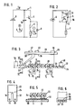
- Fig. 1 eine bekannte Chopper-Schaltung.
- Fig. 2 die gleiche Schaltung in einer erfindungsgemäßen Ausbildung.
- Fig. 3 in Seitenansicht schematisch die Ausbildung eines Transistorschalters gemäß der Erfindung.
- Fig. 4 in Draufsicht ein Detail des Schalters nach Fig. 3, und zwar den Anschluß für einen Stützkondensator.
- Fig. 5 schematisch einen Schnitt längs der Linie V-V in Fig. 3.
- Fig. 6 einen Schnitt längs der Linie VI-VI in Fig. 3.
- Fig. 7 in Draufsicht eine Leiterausbildung für eine Schaltanordnung nach Fig. 3.
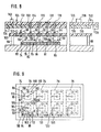
- Fig. 8 in Seitenansicht ein Halbleiter-Modul.
- ig. 9 eine Draufsicht auf das Mehrfach-Halbleiter-Modul nach Fig. 8.
- Fig. 10 eine bekannte Wechselrichterschaltung.
- Fig. 11 eine Wechselrichterschaltung gemäß der Erfindung.
- Fig. 12 eine weitere Ausgestaltung der Wechselrichterausbildung nach Fig. 11.
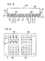
- Fig. 13 eine Ausbildung des Mehrfach-Moduls für einen Wechselrichter nach Fig. 11 oder 12.
- Fig. 14 eine Anordnung der Halbleiterschaltelemente und der Dioden in einem Mehrfach-Modul für einen Wechselrichter nach Fig. 11 oder 12.
- Fig. 1 shows a known chopper circuit.
- Fig. 2 shows the same circuit in an embodiment of the invention.
- Fig. 3 in side view schematically the formation of a transistor switch according to the invention.
- Fig. 4 in plan view a detail of the switch of Fig. 3, namely the connection for a backup capacitor.
- 5 schematically shows a section along the line VV in FIG. 3.
- 6 shows a section along the line VI-VI in FIG. 3rd
- 7 shows a top view of a conductor formation for a switching arrangement according to FIG. 3.
- Fig. 8 in side view of a semiconductor module.
- ig. 9 shows a plan view of the multiple semiconductor module according to FIG. 8.
- 10 shows a known inverter circuit.
- 11 shows an inverter circuit according to the invention.
- 12 shows a further embodiment of the inverter design according to FIG. 11.
- 13 shows an embodiment of the multiple module for an inverter according to FIG. 11 or 12.
- 14 shows an arrangement of the semiconductor switching elements and the diodes in a multiple module for an inverter according to FIG. 11 or 12.
Der Schaltkreis nach Fig. 1 weist eine induktive Last 2 auf, die in Reihe mit einem Schalttransistor 4 angeordnet ist, über den die Last periodisch aus einer Spannungsquelle 6 mit Strom versorgt wird. Parallel zur Last 2 ist eine Freilaufdiode 8 angeordnet. Die Freilaufdiode ist im wesentlichen für die gleiche Leistung ausgelegt wie der Transistor und im nachstehenden kurz als Diode bezeichnet. Bei durchgeschaltetem Transistor 4 tritt ein Fluß Φ1 auf, der die Leiterschleifenebene gebildet aus dem Transistor 4, der Last 2 und der Stromquelle 6 nach unten verläßt, wie durch den Pfeil angedeutet. Dieser Kreis hat eine Schleifeninduktivität L . Wenn der Transistor 4 sperrt, wird durch die Induktivität der Last 2 ein Fluß Φ2 erzeugt, der aus der Leiterschleifenebene gebildet aus der Last 2 und der Diode 8 nach oben austritt, wie durch Pfeil angedeutet. Beim Ausschalten des Transistors 4 wird durch den ersten Leiterkreis durch die Schleifeninduktivität ein Strom getrieben, der über den Transistor 4 eine Spannung U erzeugt. Diese Spannung ergibt sich aus der Formel1 has an inductive load 2, which is arranged in series with a

Beim Abschalten eines Stromes von 5 A in 1 µs ergibt sich an einer solchen Induktivität eine Überspannung von
Diese Spannung, die die zulässige Überspannung eines Transistors überschreitet, wird dadurch begrenzt, daß in dem Leiterkreis 1 ein Stützkondensator 10 parallel zur Last 2 und zum Transistor 4 geschaltet wird. Durch diesen Stützkondensator wird die für den Kommutierungsvorgang wirksame Leiterschleife reduziert auf die durch den Stützkondensator 10, den Transistor 4 und die Last 2 gebildete Schleife. Die im Abschaltkreis vorhandene Induktivität reduziert sich dadurch etwa um eine Größenordnung auf etwa 2.5 µH bis 10 pH. Die zu erwartende Überspannung ist dann unter sonst gleichen Bedingungen 12.5 V bis 50 V.This voltage, which exceeds the permissible overvoltage of a transistor, is limited in that a supporting
Die Möglichkeit, den Transistor durch einen solchen Stützkondensator zu schützen, ist begrenzt einmal durch die vom Transistor zu schaltenden Ströme und zum andern durch die Schaltzeit. Schon eine Vergrößerung des zu schaltenden Stroms auf 100 A ergibt unter Zugrundelegung der übrigen Parameter eine Überspannung von max. 1000 V. Wird bei einer solchen Stromstärke weiter die Schaltzeit um eine Größenordnung auf beispielsweise 100 ns herabgesetzt, ergibt sich eine Überspannung von max.. 10000 V. In beiden Fällen ist es nicht mehr möglich, die überspannung am Transistor durch einen Stützkondensator in der nach Fig. 1 beschriebenen Art zu begrenzen.The possibility of protecting the transistor by such a backup capacitor is limited on the one hand by the currents to be switched by the transistor and on the other hand by the switching time. Even increasing the current to be switched to 100 A, based on the other parameters, results in an overvoltage of max. 1000 V. If the switching time is further reduced by an order of magnitude to, for example, 100 ns at such a current, an overvoltage of max. 10000 V results. In both cases it is no longer possible to compensate for the overvoltage at the transistor by means of a backup capacitor Fig. 1 described limit.
Fig. 2 zeigt eine Schaltung, bei der bei hohen Strömen, beispielsweise in der genannten Größenordnung von 100 A und Schaltzeiten in der Größenordnung von 100 ns, das Entstehen extremer überspannungen vermieden wird. Bei der Ausführungsform nach Fig. 2 sind im Prinzip die gleichen Leiterkreise vorgesehen, wie bei der Ausführungsform nach Fig. 1. Abweichend sind hier der Transistor 4 und die Diode 8, die bezogen auf den gemeinsamen Anschluß 12 an die Last - Lastpunkt - gleichsinnig vom Strom durchflossen werden, in unmittelbarer Nachbarschaft angebracht, wie durch den gestrichelt dargestellten Rahmen 14 angedeutet. Auf diese Weise tritt eine sehr enge magnetische Kopplung der stromführenden Leiter des Transistors und der Diode 8 auf. Die aus Stromquelle 6, Transistor 4 und Last 2 bestehende Leiterschleife kann jetzt als Bestandteil der Lastinduktivität aufgefaßt werden. Für den Schaltvorgang ist nur noch die Induktivität der aus der Spannungsquelle 6, dem Transistor 4 und der Diode 8 gebildeten Leiterschleife wirksam. Die Induktivität läßt sich noch weiter verringern, wenn der Stützkondensator 10 unmittelbar zwischen die Anschlüsse 14 und 16 des durch den Transistor 4 und die Diode 2 gebildeten Moduls 18 geschaltet wird. Die beiden zur Spannungsquelle 6 führenden Leiter sind, wie in der Zeichnung durch die enge Parallelführung angedeutet, so eng wie möglich aneinanderliegend geführt und damit magnetisch eng gekoppelt. Die wirksamen Induktivitäten können dabei bis in die Größenordnung von 10 nH verringert werden. Damit ergeben sich auch bei den genannten extrem kurzen Schaltzeiten Überspannungen; die in bekannter Weise wiederum durch einen einfachen Stützkondensator begrenzt werden können. Unter Einbezug der Induktivität des Stützkondensators läßt sich eine Gesamtinduktivität von nur etwa 20 nH erreichen und somit für einen in 100 ns zu schaltenden Strom von 100 A die Überspannung auf etwa 20 V begrenzen.2 shows a circuit in which the occurrence of extreme overvoltages is avoided at high currents, for example in the order of 100 A mentioned and switching times in the order of 100 ns. In principle, the same conductor circuits are provided in the embodiment according to FIG. 2 as in the embodiment according to FIG. 1. The
Die engste Parallelführung und magnetische Kopplung ist erreichbar, wenn Transistor und Diode auf einem Chip angeordnet sind. Auf einem Chip können dabei auch mehrere Transistoren und Dioden jeweils nebeneinander angeordnet werden. Eine solche Parallelschaltung ist im allgemeinen erforderlich, wenn hohe Ströme zu schalten sind. Den Forderungen kann aber auch in ausreichendem Maße dadurch Rechnung getragen werden, daß die Transistoren und die Dioden auf eigenen Chips wechselweise nebeneinander auf einer gemeinsamen Grundplatte, die als Wärmesenke dient, angeordnet werden, wobei es auch möglich ist, diskrete Transistoren und Dioden in zwei gesonderten Reihen anzuordnen. Besonders vorteilhaft ist es, wenn die Halbleiterelemente gegen die gemeinsame Grundplatte isoliert aufgebracht werden, was z.B. durch thermisch gut leitende Isolierschichten aus Berylliumoxyd oder Aluminiumoxyd erfolgen kann. Ein extrem niederinduktiver schneller Schalter für induktive Lasten ist in Fig. 3 schematisch dargestellt. Um die Induktivität der Leiter möglichst gering zu halten, sind die Leiter im Bereich der Anschlüsse der Transistoren und Dioden als Schichtung von drei dünnen, durch Isolierschichten getrennte Leiterbahnen ausgebildet. Diese Leiterbahnen sind vorzugsweise streifenförmig und können beispielsweise aus dünnen Kupferblechen bestehen. Die drei in Fig. 3 dargestellten Leiterschichten 20, 22, 24 sind durch die Isolier-, schichten 21, 23 voneinander getrennt, die in der Zeichnung übertrieben dick dargestellt sind. Diese Isolierschichten sollten so dünn wie möglich ausgebildet sein. Die oberste Leiterschicht 20 ist hier der Lastanschluß. Diese Leiterschicht ist an einem Ende abgewinkelt, wobei der abgewinkelte Abschnitt 26 eine Anschlußfahne bilden kann, die beispielsweise an der Unterseite einer aus Isoliermaterial bestehenden Anschlußtragplatte 28 anliegen kann und durch eine Schraube mit einem oben auf der Platte 28 liegenden Anschlußpol 30 verbunden ist.The closest parallel guidance and magnetic coupling can be achieved if the transistor and diode are arranged on one chip. Several transistors and diodes can also be arranged side by side on a chip. Such a parallel connection is generally required when high currents are to be switched. However, the requirements can also be sufficiently taken into account by arranging the transistors and the diodes on their own chips alternately side by side on a common base plate, which serves as a heat sink, it also being possible to use discrete transistors and diodes in two separate ones Arrange rows. It is particularly advantageous if the semiconductor elements are applied in an insulated manner against the common base plate, which can be done, for example, by thermally highly conductive insulating layers made of beryllium oxide or aluminum oxide. An extremely low-inductance, fast switch for inductive loads is shown schematically in FIG. 3. In order to keep the inductance of the conductors as low as possible, the conductors are in the area of the connections of the transistors and diodes as a layering of three thin ones by Iso lierschichten formed separate conductor tracks. These conductor tracks are preferably strip-shaped and can consist, for example, of thin copper sheets. The three
Die darunter liegenden Leiterschichten 32 und 34 sind mit der Gleichstrom-Spannungsquelle verbunden. Die beiden Leiter sind an ihrem linken Ende umgebogen und nach oben geführt, wo sie gleichfalls an ihren Enden mit Laschen 36, 38 von unten gegen die Platte 28 anliegen und über Schrauben mit auf der Oberseite der Platte 28 liegenden Polanschlüssen 40, 42 verbunden sind. Die Lastanschlüsse der Transistoren Ti-Tx und der Dioden D1-DX, von denen in der Anlage eine entsprechende Anzahl nebeneinander angeordnet sind, sind mit der Leiterschicht 20 verbunden. Die Transistoren sind drain- bzw. kollektorseitig an die Leiterschicht 32 angeschlossen, während die Dioden mit ihrem zweiten Pol an die Leiterschicht 34 angeschlossen sind.The underlying conductor layers 32 and 34 are connected to the DC voltage source. The two conductors are bent over at their left end and led upwards, where they likewise rest at their ends with
Wie erwähnt, können die einzelnen Leiterschichten 20, 22, 24 aus Blechstreifen bestehen. Zum Anschluß eines Stützkondensators können die beiden Leiterschichten, die an die Spannungsquelle angeschlossen sind, an einem Ende, bei der Ausführungsform beispielsweise am rechten Ende in Form von getrennten Anschlußfahnen 32, 34 weitergeführt sein. Eine solche Ausbildung von Leiterfahnen ist in Fig. 4 in Draufsicht dargestellt. Die Leiterfahnen haben hier beispielsweise eine Breite, die etwas weniger als die halbe Breite der Leiterschichten beträgt. Die nebeneinanderliegenden Anschlußfahnen können in eine Ebene gebogen sein. Sie sind mit Anschlußbohrungen 44, 46 versehen, durch die die Anschlußschrauben eines Stützkondensators hindurchführbar sind. Auf diese Weise wird der Stützkondensator elektrisch angeschlossen und gleichzeitig mechanisch gehaltert. Ein solcher Stützkondensator 48 sollte möglichst nahe an den freien, d.h. von der Last abgewandten Anschlüssen 32, 34 von Transistoren und Dioden liegen, um zu einer Leiterschleife geringer Induktivität zu kommen. Entsprechende Anschlußfahnen können am gegenüberliegenden Ende vorgesehen sein. Es sind dann die beiden Leiterschichten 22, 24 entsprechend weiterzuführen. Die zum Anschluß 40 führende Anschlußfahne 50 kann dann, wie gestrichelt dargestellt, mit ihrem den Leiterschichten zugewandten Ende auf der Oberseite der Leiterschicht 22 elektrisch leitend befestigt sein. Die Anschlußfahne, die zu dem Anschlußpol 42 führt, kann mit einem die Leiterschichten 22 und 24 seitlich umgreifenden Ansatz versehen sein, der dann elektrisch leitend an der Unterseite der Leiterschicht 24 befestigt sein kann. Auf den so auch links herausgeführten Leiterfahnen kann ein weiterer Stützkondensator 54 angeordnet sein.As mentioned, the individual conductor layers 20, 22, 24 can consist of sheet metal strips. To connect a backup capacitor, the two conductor layers, which are connected to the voltage source, can be continued at one end, in the embodiment, for example, at the right end in the form of separate connecting
Die Anschlußfahnen an den beiden Enden können gleichzeitig auch als Anschlüsse an die Spannungsquelle dienen. In diesem Fall würden die nach oben zu den Anschlußpolen 40 und 42 führenden Anschlußfahnen entfallen.The connection lugs at the two ends can also serve as connections to the voltage source. In this case, the connection lugs leading up to the
Wie aus Fig. 5 ersichtlich, sind die Chips mit den Dioden D und mit den Transistoren T auf einer Substratplatte 56 und mit dieser auf einer als Wärmesenke wirkende Metallplatte 58 befestigt. Bei dieser Anordnung liegen eine Mehrzahl von Transistoren in einer Reihe und parallel dazu liegt eine Reihe von Dioden. In Fig. 5 ist weiter schematisch dargestellt, wie die Dioden bzw. Transistoren mit den Leiterschichten 20, 22 und 24 verbunden sind.5, the chips with the diodes D and with the transistors T are fastened on a
Ein Schalter, wie er in-Fig. 3 schematisch dargestellt und im vorstehenden beschrieben worden ist, läßt sich so ausbilden, daß er einschließlich der Induktivität eines Stützkondensators eine Gesamtinduktivität von 20 nH und weniger aufweist.A switch as shown in Fig. 3 has been shown schematically and described above, can be designed so that it has a total inductance of 20 nH and less, including the inductance of a backup capacitor.
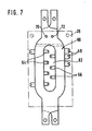
Die Bond-Drähte der Transistoren und Dioden können direkt mit den betreffenden Leiterschichten verbunden werden. Hierzu werden zweckmäßig an den Leiterschichten, also beispielsweise an den die Leiterschichten bildenden Blechstreifen, vorstehende Anschlußelemente vorgesehen, die auch auf beiden Längsseiten angeordnet sein können. Eine weitere Möglichkeit besteht, die Leiterschichten in der Mitte mit einem Längsschlitz zu versehen, wie beispielsweise in Fig. 7 veranschaulicht. Die Leiterschichten 60 sind hier im Bereich der Transistoren und Dioden in der Mitte mit einem länglichen Ausschnitt 62 versehen, in die von zwei der Leiterschichten Anschlußelemente 64, 66 vorstehen. An der dritten Leiterschicht sind Anschlußelemente 68 vorgesehen. Wenn die außen liegenden Anschlußelemente bei einer Anordnung der Chips entsprechend Fig. 5 an der den Lastanschluß bildenden Leiterschicht angeordnet sind, kann es zweckmäßig sein, entsprechende Anschlußfahnen auch in der gegenüberliegenden Seite vorzusehen, so daß für die Bond-Drähte der Si-Chips und der Transistor-Chips jeweils eigene Anschlußelemente zur Verfügung stehen, wodurch die Montage erleichtert werden kann.The bond wires of the transistors and diodes can be connected directly to the relevant conductor layers. For this purpose, projecting connection elements are expediently provided on the conductor layers, that is to say, for example, on the sheet metal strips forming the conductor layers, which can also be arranged on both longitudinal sides. Another possibility is to provide the conductor layers with a longitudinal slot in the middle, as illustrated for example in FIG. 7. The conductor layers 60 are provided in the area of the transistors and diodes in the middle with an
Wie in Fig. 7 angedeutet, können in den Leiterschichten Bohrungen 70, 72 vorgesehen sein, durch die Leiter für den Steueranschluß der Transistoren hindurchgeführt werden können.As indicated in FIG. 7, holes 70, 72 can be provided in the conductor layers through which conductors for the control connection of the transistors can be passed.
Grundsätzlich können für Schalter der beschriebenen Art normale schnellwirkende Schalttransistoren vorgesehen sein. Vorzugsweise werden jedoch Feldeffekttransistoren verwendet.In principle, normal, fast-acting switching transistors can be provided for switches of the type described. However, field effect transistors are preferably used.
Wie oben beschrieben, können die Leiterschichten aus Blechstreifen mit dazwischen liegenden Isolationen aufgebaut werden. Es ist selbstverständlich auch möglich, die Leiterschichten nach Art einer mehrschichtigen Leiterplatte auszubilden. Wesentlich ist, daß die Leiterschleife mit den Leiterschichten, mit denen die Transistoren bzw. die Dioden mit ihren dem gemeinsamen Anschluß an die Last entgegengesetzten Anschlüssen verbunden sind, dadurch eine möglichst geringe Induktivität hat, daß diese Leiterschichten so eng wie möglich aneinanderliegen.As described above, the conductor layers can be constructed from sheet metal strips with insulation in between. It is of course also possible to design the conductor layers in the manner of a multilayer printed circuit board. It is essential that the conductor loop with the conductor layers with which the transistors or diodes are connected with their connections opposite the common connection to the load has the lowest possible inductance in that these conductor layers lie as closely as possible to one another.
Die Lage der den Lastanschluß bildenden Leiterplatte 20 ist unkritisch. Diese kann auch in größerem Abstand von den Leiterplatten 22 und 24 liegen und muß nicht unbedingt parallel zu diesen liegen. So kann beispielsweise zwischen der Leiterplatte 22 und dem Lastanschluß eine Leiterplatte mit den Steueranschlüssen für die Transistoren angeordnet sein, über der die Leiterplatte in Abstand gehaltert ist.The position of the
In Fig. 8 und 9 ist schematisch ein Halbleitermodul mit einer Mehrzahl von Transistoren und Dioden dargestellt. Auf einer Kupferplatte 74 als Wärmesenke ist eine Mehrzahl von Chipträgerplatten 76 aufgelötet, die aus einem beidseitig mit einer Kupferschicht 78, 80 kaschierten Platte 82 aus Aluminiumoxid besteht. Die Chipträgerplatte ist mit ihrer Kupferschicht 78 mit der Wärmesenke 74 verlötet. Auf der oberen Kupferschicht sind wenigstens ein Transistorchip 84 und ein Diodenchip 86, vorzugsweise eine Mehrzahl davon, aufgelötet. Eine derartige Mehrzahl von Transistoren und Dioden ist im nachstehenden als Grundmodul bezeichnet.8 and 9 schematically show a semiconductor module with a plurality of transistors and diodes. A plurality of
Die Transistoren und/oder die Dioden eines Grundmoduls können auch auf mehr als einem Chipträger angeordnet werden. Die Kupferschicht 80 ist dabei gemeinsamer Anschlußpunkt für die Transistoren und die Dioden. Die einzelnen Anschlüsse für die Basis B, den Kollektor C und den Emitter des Transistors sind mit Bonddrähten 88, 90, 92 kontaktiert und der zweite Anschluß der Diode 86 mit einem Bonddraht 94.The transistors and / or the diodes of a basic module can also be arranged on more than one chip carrier. The
Sofern freibleiben soll, ob die Diode mit ihrer Kathode oder ihrer Anode mit dem gemeinsamen Lastpunkt verbunden werden soll, kann die Kupferschicht 80 zwischen den Transistorchips 84 und den Diodenchips 86 getrennt sein, wie in Fig. 8 durch den Trennstrich 81 angedeutet. Es ist dann für den Diodenchip 86 ein weiterer Bonddraht 96 vorzusehen.If it remains to be seen whether the diode is to be connected to the common load point with its cathode or its anode, the
Da die beispielsweise aus Aluminium bestehenden Bonddrähte nur eine geringe Steifigkeit haben, ist es zweckmäßig, sie mit starren Anschlüssen, beispielsweise Anschlußstiften, zu verbinden, über die dann die Verbindungen zu den Leiterschichten hergestellt werden. Die Anschlüsse, die mit der Kupferschicht 80 zu verbinden sind, können mit dieser verlötet und dann auch starr ausgebildet sein.Since the bonding wires, for example made of aluminum, have only a low rigidity, it is expedient to connect them to rigid connections, for example connecting pins, via which the connections to the conductor layers are then made. The connections which are to be connected to the
In Fig. 8 ist lediglich ein Chipträger mit einem Transistorchip und einem Diodenchip dargestellt. Wie in Fig. 9 dargestellt, werden vorzugsweise mehrere Chipträger verwendet und auf jedem Chipträger sind vorzugsweise mehrere Transistoren und Dioden angeordnet. Weitere Chipträger sind in Fig. 8 als Blöcke gestrichelt dargestellt.8 only shows a chip carrier with a transistor chip and a diode chip. As shown in FIG. 9, a plurality of chip carriers are preferably used, and a plurality of transistors and diodes are preferably arranged on each chip carrier. Further chip carriers are shown in broken lines in FIG. 8.
Oberhalb der Chips 84 und 86 ist auf Stützen 98 eine Leiterplatte 100 gehaltert. Diese Leiterplatte ist mit Bohrungen 102 bis 110 versehen, deren Durchmesser groß ist im Verhältnis zum Durchmesser der Bonddrähte 88 bis 96. Neben den Bohrungen 102 bis 110 sind jeweils Anschlußstifte 112, 114, 116, 118 und 119 vorgesehen. Zur Befestigung der Anschlußstifte können an der Unterseite der Leiterplatte 100 diskrete Lötpunkte vorgesehen sein.A printed
Von den Chipträgern 76 können, wie in Fig. 9 schematisch dargestellt, eine Mehrzahl nebeneinander angeordnet sein, wobei in Fig. 9 die Chipträger 76 jeweils gegenüber der Darstellung in Fig. 8 um 90° gedreht wiedergegeben sind. Eine weitere Anordnung der Chipträger ist in Fig. 14 wiedergegeben, die weiter unten beschrieben wird.As schematically shown in FIG. 9, a plurality of the
Nach dem Verbinden der Bonddrähte mit den Chips 84 und 86 werden diese senkrecht nach oben ausgerichtet. Es ist dann leicht möglich, auch bei einer großen Zahl von Bonddrähten diese beim Aufsetzen der Leiterplatte 100 durch die relativ großen Bohrungen 102 bis 110 hindurchzuführen. Nach dem Aufsetzen der Leiterplatte 100 werden die Bonddrähte dann mit den Anschlußstiften in bekannter Technik leitend verbunden. Der Anschluß der Bonddrähte an die Anschlußstifte erfolgt zweckmäßig so, daß ein Ausgleich thermisch bedingter Längenänderungen möglich ist. Nachdem die Verbindung zu den Verbindungsstiften hergestellt ist, können die Chips unter der Leiterplatte 100 durch Ausgießen des Zwischenraumes zwischen der Leiterplatte 100 und der Wärmesenkeplatte 74 geschützt werden.After the bonding wires have been connected to the
Die Anschlußstifte 112 für die Basis B der Transistoren 84 werden zweckmäßig kürzer ausgebildet als die übrigen Anschlußstifte. An der Unterseite der Leiterplatte 100 können, wie in Fig. 9 angedeutet, Leiterbahnen 120 vorgesehen werden, an die die Basisanschlüsse der Transistoren 84 angeschlossen sind, und zwar vorzugsweise über Vorwiderstände 122, die beim Verlöten der Kontaktstifte gleichzeitig mitverlötet werden. Der Lötpunkt für die Anschlußstifte 112 kann dabei gleichzeitig für den Anschluß des Vorwiderstandes 122 ausgebildet sein. Für jedes Grundmodul wird zweckmäßig eine Leiterbahn vorgesehen, um die Grundmodule wahlweise ansteuern zu können.The
Bei der weiter unten zu beschreibenden Schaltung für einen Wechselrichter werden Grundmodule mit Transistoren und Dioden benötigt, bei denen die Dioden an dem gemeinsamen Lastpunkt einmal mit der Anode und zum andern mit der Kathode angeschlossen sind. In diesem Fall wird der Mehrfach-Modul nach Fig. 8 und 9 vorzugsweise mit vier Grundmoduln versehen, und zwar zwei, bei denen die Dioden mit der Anode und zwei, bei denen die Dioden mit der Kathode am Lastpunkt liegen. Sofern auf einem Chipträger eine Mehrzahl von Transistor- und Diodenchips angeordnet ist, kann jeweils auch eine Mehrzahl von Bonddrähten paralleler Pole auf einen Anschlußstift geführt werden.In the circuit for an inverter to be described below, basic modules with transistors and diodes are required, in which the diodes are connected to the common load point on one side with the anode and on the other side with the cathode. In this case, the multiple module according to FIGS. 8 and 9 is preferably provided with four basic modules, two in which the diodes with the anode and two in which the diodes with the cathode are at the load point. If a plurality of transistor and diode chips are arranged on a chip carrier, a plurality of bonding wires of parallel poles can in each case also be guided on a connecting pin.
Ein Mehrfach-Modul nach Fig. 8 und 9 mit einer Mehrzahl von Grundmoduln kann für den jeweiligen Anwendungszweck über eine entsprechend ausgebildete Leiterplatte verschaltet werden. Eine solche Leiterplatte ist, wie es in Fig. 8 und 9 dargestellt ist, zweckmäßig als eine Mehrschichtleiterplatte 124 ausgebildet. Diese Platte ist hier mit drei Dickschichtleiterschichten 126, 128, 130 und mit Bohrungen 132 entsprechend dem Raster der Anschlußstifte 114 bis 118 des Mehrfach-Moduls versehen. Diese Bohrungen 132 sind jeweils durchkontaktiert, und zwar mit Anschluß an die jeweils gewünschte Leiterebene 126, 128 bzw. 130. Bei dem dargestellten Ausführungsbeispiel ist der Leiter in der Leiterebene 126 der Lastanschluß, der Leiter in der Leiterebene 128 der Plus-Pol und der Leiter in der Leiterebene 130 der Minus-Pol. Die Leiter in den Leiterebenen 128, 130 können jeweils an den Enden mit Anschlüssen 134, 136 für den Anschluß der Gleichspannung versehen werden, während der Leiter in der Leiterebene 126 mit einem Lastanschluß 138 versehen ist. An den Enden der Leiterebenen 128, 130 können weiter Anschlüsse für die Stützkondensatoren 140, 142 vorgesehen sein. In den einzelnen Leiterebenen können auch parallele Leiterbahnen ausgebildet sein.A multiple module according to FIGS. 8 and 9 with a plurality of basic modules can be connected for the respective application via an appropriately designed printed circuit board. Such a printed circuit board, as shown in FIGS. 8 and 9, is expediently designed as a multilayer printed
Wie aus dem vorstehenden ersichtlich, lassen sich Mehrfach-Moduln, wie sie im vorstehenden beschrieben sind, in unterschiedlicher Weise verschalten, wobei diese Verschaltung ausschließlich über die Leiterplatte 124 erfolgt. Diese Leiterplatte kann leicht auf die Anschlußstifte des Mehrfach-Moduls aufgesteckt werden. Die Anschlußstifte brauchen dann lediglich in den durchkontaktierten Bohrungen verlötet zu werden. Die Leiterplatte 124 ergibt wie die Leiterausbildung nach den Fig. 3 bis 6 einen extrem induktivitätsarmen Schaltkreis, und zwar auch dann, wenn die den Lastanschluß bildende Leiterschicht der Platte 126 in größerem Abstand von oder in anderer Lage relativ zu den Leiterschichten 128 und 130 angeordnet ist.As can be seen from the foregoing, multiple modules, as described in the foregoing, can be interconnected in different ways, this interconnection taking place exclusively via the printed
Der vorstehend beschriebene Mehrfach-Modul eignet sich in besonderer Weise auch für Brückenschaltungen, wie sie z.B. für Wechselrichter angewendet werden.The multiple module described above is also particularly suitable for bridge circuits, such as those e.g. can be used for inverters.
Eine bekannte Wechselrichterschaltung ist in Fig. 10 dargestellt. Sie besteht aus vier Halbleiterschaltelementen, hier Transistoren T1, T1', T2 und T2' sowie aus vier Dioden D1, D1', D2 und D2'. Die Last L ist als ohmsch-induktive Last dargestellt. Sie kann beispielsweise ein Transformator sein. Der Wechselrichter wird aus einer Gleichstromspannungsquelle B gespeist und weist einen zwischen die Speiseleitungen geschalteten Stützkondensator C auf.A known inverter circuit is shown in FIG. 10. It consists of four semiconductor switching elements, here transistors T1, T1 ', T2 and T2' as well as four diodes D1, D1 ', D2 and D2'. The load L is shown as an ohmic-inductive load. For example, it can be a transformer. The inverter is fed from a DC voltage source B and has a backup capacitor C connected between the feed lines.
Zum Betrieb des Wechselrichters werden über eine nicht dargestellte Steuerung bei Beginn einer Halbwelle z.B. die Transistoren T1 und T1' angesteuert. Der Strom fließt dann von der Spannungsquelle B über Transistor T1 zur Last L und über Transistor T1' zurück zur Spannungsquelle. Nach dem Abschalten der Transistoren T1, T1' wird der Strom durch die in der Induktivität der Last gespeicherte magnetische Energie weiter aufrechterhalten und fließt über die Dioden D1 und D1' zurück zur Spannungsquelle. Gleichzeitig werden die Transistoren T2 und T2' leitend gesteuert, so daß sich der Strom nach seinem Abklingen in der Last umkehrt und dann während der zweiten Halbwelle von der Batterie über die Transistoren T2 und T2' fließt. Nach Ablauf dieser Halbwelle wiederholt sich der gleiche Vorgang. Die Transistoren T2 und T2' werden wieder abgeschaltet, der Strom fließt in gleicher Richtung über die Dioden D2 und D2' zurück zur Spannungsquelle bis nach Einschalten der Transistoren T1 und T1' der Strom wieder über diese fließt. Benachbarte Transistoren und Dioden mit gleichem Last- und Gleichspannungsanschluß werden hier gegensinnig vom Strom durchflossen.For the operation of the inverter, for example, the trans sistors T1 and T1 'driven. The current then flows from voltage source B via transistor T1 to load L and via transistor T1 'back to the voltage source. After switching off the transistors T1, T1 ', the current is further maintained by the magnetic energy stored in the inductance of the load and flows back to the voltage source via the diodes D1 and D1'. At the same time, the transistors T2 and T2 'are turned on, so that the current reverses after it has decayed in the load and then flows through the transistors T2 and T2' from the battery during the second half-cycle. After this half-wave, the same process is repeated. The transistors T2 and T2 'are switched off again, the current flows in the same direction via the diodes D2 and D2' back to the voltage source until after switching on the transistors T1 and T1 'the current again flows through them. Adjacent transistors and diodes with the same load and DC voltage connection are flowed through in opposite directions by the current.
Für die Kommutierung des Laststromes aus den Transistorzweigen in die Diodenzweige ergibt sich das gleiche Problem, wie oben für die Chopper-Schaltung beschrieben. Auch bei der Brückenschaltung nach Fig. 10 durchfließt der Strom jeweils in entgegengesetzter Richtung unterschiedliche, räumliche Leiterschleifen, welche beim Kommutierungsvorgang erhebliche die Transistoren gefährdende Spannungsspitzen im Kommutierungskreis erzeugen können. Durch den Stützkondensator C kann lediglich die Auswirkung der Induktivität der Zuleitungsschleife von der Gleichspannungsquelle bis zum Wechselrichter eliminiert werden.The same problem arises for the commutation of the load current from the transistor branches into the diode branches as described above for the chopper circuit. Also in the bridge circuit according to FIG. 10, the current flows through different, spatial conductor loops in the opposite direction, which can generate considerable voltage peaks in the commutation circuit which endanger the transistors during the commutation process. The support capacitor C can only eliminate the effect of the inductance of the supply loop from the DC voltage source to the inverter.
Bei der erfindungsgemäß ausgebildeten Brückenschaltung nach Fig. 11 sind im Gegensatz zu der Schaltung nach Fig. 10, bei der benachbarte Transistoren und Dioden gegensinnig vom Strom durchflossen sind, die Dioden den Transistoren jeweils so zugeordnet, daß beide gleichsinnig vom Strom durchflossen werden. Bei dieser Anordnung gibt es damit keine Leiterschleifen mehr, die abwechselnd in entgegengesetztem Sinne vom Strom durchflossen werden, wie bei der Ausführungsform nach Fig. 10. Dadurch, daß der Strom jeweils im gleichen Sinne umläuft, wird in Verbindung mit den auch hier, wie oben unter Bezug auf Fig. 1 bis 9 beschrieben, eng benachbart geführten Leitern eine sehr niedrige parasitäre Induktivität der Schaltung erzielt. Die enge Leiterführung braucht hier nur bis zum Stützkondensator C geführt zu werden, wenn dieser niederohmig ist. Damit läßt sich diese Schaltung in besonders zweckmäßiger Weise mit einem Mehrfach- Modul gemäß der Erfindung realisieren.11, in contrast to the circuit according to FIG. 10, in which adjacent transistors and diodes are through in opposite directions from the current are flowed, the diodes are assigned to the transistors so that the current flows through both in the same direction. In this arrangement, there are no longer any conductor loops which are alternately flowed through by the current in the opposite sense, as in the embodiment according to FIG. 10. Because the current flows in the same sense in each case, in connection with those here, as above described with reference to FIGS. 1 to 9, closely guided conductors achieved a very low parasitic inductance of the circuit. The narrow conductor routing only needs to be carried up to the support capacitor C if it has a low resistance. This circuit can thus be implemented in a particularly expedient manner with a multiple module according to the invention.
Eine weitere Verringerung der störenden parasitären Induktivität wird dadurch erreicht, daß der Stützkondensator aufgeteilt wird in vier Teilkondensatoren C1 C2, c21 und C1" die jeweils in unmittelbarer Nähe der Grundmodule 150, 152 angeordnet sind. Störend im Sinne der Entstehung einer parasitären Induktivität ist dann lediglich nur noch die Leiterschleife, bestehend aus Transistor, Diode und Kondensator, die durch den oben beschriebenen Aufbau eines Mehrfach-Moduls hinreichend klein gemacht werden kann. Die in den Fig. 11 und 12 dargestellten Grundmoduln 150 bzw. 152 weisen vorzugsweise eine Mehrzahl von parallelen Transistoren und Dioden im Sinne der obigen Ausführungen auf.A further reduction in the disturbing parasitic inductance is achieved in that the backup capacitor is divided into four partial capacitors C 1 C 2 , C 21 and C 1 ", which are each arranged in the immediate vicinity of the
Um bei den Schaltungen nach den Fig. 11 und 12 einen Kurzschlußstrom zu vermeiden, der dann auftritt, wenn mit dem Ausschalten des Transistors in dem einen Stromweg gleichzeitig der Transistor im anderen Stromweg eingeschaltet wird, beispielsweise T1 und T1' ausgeschaltet und gleichzeitig T2 und T2' ausgeschaltet werden, ist es notwendig, zwischen diesen und den Lastpunkten der Grundmodule 150 und 152 jeweils eine Induktivität vorzusehen. Bei den kurzen Schaltzeiten in der Größenordnung von 100 ns und den großen Stromstärken genügt hier eine Induktivität von wenigen nH. Die Induktivität kann beispielsweise durch eine Leiterschleife gebildet werden, wie sie in Fig. 13 dargestellt ist. In dieser Zeichnung ist das Mehrfach-Modul lediglich durch die beiden unterschiedlichen Grundmodule angedeutet, also durch Module, bei denen die Diode einmal mit ihrer Anode und zum andern mit ihrer Kathode am Lastpunkt liegt. Die Leiterplatte ist hier wieder mit den Leiterschichten 126, 128, 130 schematisch dargestellt. An den Leiterschichten liegt die Gleichspannung an, und zwar mit dem Minus-Pol an der Leiterschicht 130 und dem Plus-Pol an der Leiterschicht 128. Die Leiterschicht 126 für den Lastanschluß ist hier in zwei elektrisch getrennte Leiterabschnitte 126', 126" aufgeteilt. Diese beiden Leiterabschnitte 126' und 126" sind über eine beispielsweise in Form eines Blechbügels 153 ausgebildete Leiterschleife miteinander verbunden. Die Leiterschleife trägt mittig den Lastanschluß 138'. Die Induktivität einer solchen Leiterschleife reicht aus, um bei den gegebenen Bedingungen Kurzschlüsse beim gleichzeitigen Ein- bzw. Ausschalten der Transistoren in den Grundmoduln zu verhindern. Stützkondensatoren 140, 142 sind hier wiederum zwischen die Leiterschichten 128 und 130 geschaltet.In order to avoid a short-circuit current in the circuits according to FIGS. 11 and 12, which occurs when the transistor in the one current path is switched on at the same time as the transistor in the other current path is switched on, for example T1 and T1 'are switched off and at the same time T2 and T2 'are switched off, it is necessary to provide an inductance between each of these and the load points of the
In Fig. 14 ist eine Schaltanordnung eines Mehrfach-Moduls im Prinzip dargestellt. Es sind hier vier Grundmoduln 156 bis 162 dargestellt, die jeweils einen Chipträger aufweisen, wie er oben unter Bezug auf Fig. 8 beschrieben ist. Die Dioden 164 und die Halbleiterschaltelemente 166 sind jeweils auf elektrisch voneinander getrennten Bereichen der oberen leitenden Schicht des Chipträgers aufgelötet. Ungeachtet der Tatsache, daß einer der Anschlußpole die leitende Schicht des Chipträgers ist, sind die einzelnen Pole der Dioden und der Halbleiterschaltelemente jeweils schematisch dargestellt. Sie sind jeweils über Bonddrähte miteinander und/oder den zugehörigen Anschlußstiften verbunden. Wie ohne weiteres ersichtlich, sind alle vier Grundmoduln 156 bis 162 identisch ausgebildet. Sie können über ihre Bonddrähte auch in identischer Weise mit Anschlußstiften verbunden sein.14 shows a circuit arrangement of a multiple module in principle. Four
Die Anzahl der auf jedem der Chipträger angeordneten bzw. dem jeweiligen Grund-Modul zugeordneten Halbleiterschaltelemente 166 ergibt die Strombelastbarkeit jedes einzelnen der Grundmoduln 156 bis 162. Jedes dieser Grundmoduln kann dabei beispielsweise für eine Stromstärke von 30 A ausgelegt sein. Dann läßt sich mit einem Mehrfach-Modul, wie es in Fig. 14 dargestellt ist, bei Parallelschaltung aller Grundmoduln eine Gesamtstromstärke von 120 A schalten. Werden jeweils zwei Grundmoduln parallel geschaltet, läßt sich mit zwei derartigen Mehrfach-Moduln eine Wechselrichterschaltung nach Fig. 11 bzw. 12 nach Art einer Halbbrücke für eine Stromstärke von 60 A realisieren. Mit den vier Grundmoduln läßt sich aber auch eine vollständige Brückenschaltung für 30 A realisieren, wobei dann jeweils die Lastanschlüsse auf vier Abschnitte der Leiterplatte 126 geführt werden, die dann jeweils paarweise über eine induktive Leiterschleife entsprechend Fig. 13 miteinander verbunden sind, deren Mitte dann jeweils einen der Lastanschlußpunkte ergibt. Es braucht dann für die gesamte Schaltung lediglich noch ein einziger Stützkondensator auf dem Halbleitermodul vorgesehen zu werden. Zweckmäßig ist es jedoch, zur weiteren Verringerung der parasitären Induktivität zwei Kondensatoren vorzusehen, wie in Fig. 13 dargestellt, die dann wiederum in größter Nähe der Grundmoduln 156, 160 bzw. 158, 162 vorgesehen sein können und dann sowohl während der positiven als auch während der negativen Halbwelle wirksam sind.The number of
Durch die hohe erreichbare Schaltfrequenz von 20 kHz und darüber lassen sich mit einem Wechselrichter der beschriebenen Art in .Verbindung mit einer Pulsweitenmodulation in weitgehender Annäherung sinusförmige Ausgangsspannungen erzeugen. Es ist dabei gleichzeitig möglich, durch die hohe Zahl der Einschaltungen während einer Halbwelle Spannungseinbrüche im allgemeinen bereits innerhalb einer Halbwelle zu kompensieren und damit zu einer sinusförmigen Ausgangsspannung hoher Konstanz zu kommen.Due to the high achievable switching frequency of 20 kHz and above, sinusoidal output voltages can be generated to a large extent using an inverter of the type described in conjunction with pulse width modulation. It is also possible due to the high number of starts to compensate for voltage dips during a half-wave in general already within one half-wave and thus to achieve a sinusoidal output voltage of high constancy.
Als Halbleiterschalter können schnellschaltende bipolare Transistoren verwendet werden. Besonders zweckmäßig ist die Verwendung von MOS-FET's. Als Schaltelemente können aber auch GTO's Anwendung finden.Fast-switching bipolar transistors can be used as semiconductor switches. The use of MOS-FETs is particularly expedient. GTOs can also be used as switching elements.
Claims (16)
Applications Claiming Priority (2)
| Application Number | Priority Date | Filing Date | Title |
|---|---|---|---|
| DE3420535 | 1984-06-01 | ||
| DE3420535A DE3420535C2 (en) | 1984-06-01 | 1984-06-01 | Semiconductor module for a fast switching arrangement |
Publications (2)
| Publication Number | Publication Date |
|---|---|
| EP0166968A1 true EP0166968A1 (en) | 1986-01-08 |
| EP0166968B1 EP0166968B1 (en) | 1988-07-27 |
Family
ID=6237444
Family Applications (1)
| Application Number | Title | Priority Date | Filing Date |
|---|---|---|---|
| EP85106644A Expired EP0166968B1 (en) | 1984-06-01 | 1985-05-30 | Semiconductor module for a fast switching arrangement |
Country Status (5)
| Country | Link |
|---|---|
| US (1) | US4670833A (en) |
| EP (1) | EP0166968B1 (en) |
| JP (1) | JPS6139563A (en) |
| CA (1) | CA1255763A (en) |
| DE (2) | DE3420535C2 (en) |
Cited By (14)
| Publication number | Priority date | Publication date | Assignee | Title |
|---|---|---|---|---|
| EP0278432A1 (en) * | 1987-02-06 | 1988-08-17 | Siemens Aktiengesellschaft | Bridge arm with free-wheel diodes |
| US4809153A (en) * | 1986-03-18 | 1989-02-28 | Siemens Aktiengesellschaft | Low-inductance bus bar arrangement |
| EP0388896A2 (en) * | 1989-03-20 | 1990-09-26 | Kabushiki Kaisha Toshiba | Buffer circuit with an electrostatic protector |
| EP0427143A2 (en) * | 1989-11-07 | 1991-05-15 | IXYS Semiconductor GmbH | Semiconductor power module |
| US5164893A (en) * | 1990-07-26 | 1992-11-17 | Asea Brown Boveri Ltd. | Low inductance gto switching circuit for an inverter |
| EP0584668A1 (en) * | 1992-08-26 | 1994-03-02 | eupec Europäische Gesellschaft für Leistungshalbleiter mbH & Co. KG | Semi-conductor power module |
| EP0598563A2 (en) * | 1992-11-18 | 1994-05-25 | Fuji Electric Co. Ltd. | Semiconductor conversion device |
| EP0600179A2 (en) * | 1992-12-02 | 1994-06-08 | EXPORT-CONTOR Aussenhandelsgesellschaft mbH | Power semiconductor circuit arrangement |
| US5544035A (en) * | 1993-12-23 | 1996-08-06 | Abb Management Ag | Converter arrangement having a low-inductance commutation circuit |
| GB2311669A (en) * | 1996-03-25 | 1997-10-01 | Int Rectifier Corp | Kelvin emitter connection to reduce current flow through parasitic diode |
| EP0833422A2 (en) * | 1996-09-25 | 1998-04-01 | ABB Daimler-Benz Transportation (Technology) GmbH | Power converter |
| EP0998019A1 (en) * | 1998-10-30 | 2000-05-03 | Siemens Aktiengesellschaft | Semiconductor circuit assembly, in particular for a high current converter with low voltage intermediate circuit |
| EP1670131A2 (en) | 2004-12-09 | 2006-06-14 | Semikron Elektronik GmbH & Co. KG Patentabteilung | Power semiconductor module with reduced parasitic inductances |
| WO2022263233A1 (en) | 2021-06-16 | 2022-12-22 | Magna powertrain gmbh & co kg | Low-inductance busbar between half-bridge module and intermediate circuit |
Families Citing this family (32)
| Publication number | Priority date | Publication date | Assignee | Title |
|---|---|---|---|---|
| GB2212677B (en) * | 1987-11-16 | 1992-07-22 | Sanyo Electric Co | An electric circuit for supplying controlled frequency electric power to a load |
| JPH01236698A (en) * | 1987-11-25 | 1989-09-21 | Hitachi Ltd | Ceramic mutilayered circuit board with built-in capacitor |
| US4979089A (en) * | 1989-05-26 | 1990-12-18 | Neturen Company Limited | Method for balancing currents to switching devices |
| JPH06101928B2 (en) * | 1989-06-27 | 1994-12-12 | 東光株式会社 | Switching power supply |
| FR2652982B1 (en) * | 1989-10-11 | 1993-04-30 | Alsthom Gec | ASSEMBLY OF ELECTRONIC POWER COMPONENTS. |
| US4975824A (en) * | 1989-12-11 | 1990-12-04 | Sundstrand Corporation | Power converter circuit board |
| WO1991009460A1 (en) * | 1989-12-20 | 1991-06-27 | Sundstrand Corporation | Low inductance converter phase assembly |
| JP2692765B2 (en) * | 1989-12-22 | 1997-12-17 | 株式会社日立製作所 | Parallel circuit with diode and IGBT, module thereof, and power converter using the same |
| US5731970A (en) * | 1989-12-22 | 1998-03-24 | Hitachi, Ltd. | Power conversion device and semiconductor module suitable for use in the device |
| US5119286A (en) * | 1989-12-28 | 1992-06-02 | Sundstrand Corporation | Modular circuit board |
| US5272590A (en) * | 1990-02-12 | 1993-12-21 | Hernandez Jorge M | Integrated circuit package having an internal cavity for incorporating decoupling capacitor |
| EP0533158B1 (en) * | 1991-09-20 | 1998-07-08 | Hitachi, Ltd. | Three-phase three-level inverter device |
| US5400235A (en) * | 1992-08-07 | 1995-03-21 | International Business Machines Corp. | High frequency energy saving DC to DC power converter |
| DE59304797D1 (en) * | 1992-08-26 | 1997-01-30 | Eupec Gmbh & Co Kg | Power semiconductor module |
| JPH06233554A (en) * | 1993-01-28 | 1994-08-19 | Fuji Electric Co Ltd | Inverter device |
| DE9403108U1 (en) * | 1994-02-24 | 1994-04-14 | Siemens Ag | Low-inductance high-current busbar for converter modules |
| DE4412407C2 (en) * | 1994-04-11 | 1996-03-07 | Jungheinrich Ag | Circuit arrangement for the operation of at least one battery-operated electric motor in an industrial truck |
| DE19512679C1 (en) * | 1995-04-07 | 1996-11-21 | Abb Management Ag | Low leakage inductance conductor assembly for controllable semiconductors |
| JP3399786B2 (en) | 1996-06-04 | 2003-04-21 | シーメンス アクチエンゲゼルシヤフト | Circuit device in motor vehicle |
| US6954368B1 (en) | 1996-07-22 | 2005-10-11 | HYDRO-QUéBEC | Low stray interconnection inductance power converting molecule for converting a DC voltage into an AC voltage, and a method therefor |
| EP0895343B1 (en) * | 1997-07-28 | 2003-09-24 | STMicroelectronics S.r.l. | Sharing of external components for the control of the switching dead-time of a plurality of integrated devices cooperating in driving and R-L multiphase actuator |
| DE19732723B4 (en) * | 1997-07-30 | 2005-07-07 | Semikron Elektronik Gmbh | Low-inductance circuit arrangement |
| US6181589B1 (en) * | 1999-07-02 | 2001-01-30 | Durel Corporation | Half-bridge inverter for coupling an EL lamp to a high voltage DC rail |
| US6356043B2 (en) * | 1999-09-09 | 2002-03-12 | Matthew C. Baum | Motor controller power switch arrangement |
| JP3620415B2 (en) * | 2000-06-30 | 2005-02-16 | 株式会社村田製作所 | Isolated converter |
| JP3906440B2 (en) * | 2000-09-06 | 2007-04-18 | 株式会社日立製作所 | Semiconductor power converter |
| DE10109329C1 (en) * | 2001-02-27 | 2002-05-02 | Siemens Ag | Circuit has power stage with heat generating components mounted around component(s) that generates less heat mounted in inner region, conducting metal body mounted on cooling body |
| JP3941041B2 (en) * | 2002-03-25 | 2007-07-04 | ミネベア株式会社 | Key switch stabilizer mechanism |
| EP1825511B1 (en) * | 2004-12-17 | 2011-11-23 | Siemens Aktiengesellschaft | Semiconductor switching module |
| JP5081202B2 (en) * | 2009-07-17 | 2012-11-28 | トヨタ自動車株式会社 | Switching device |
| DE102010002627B4 (en) | 2010-03-05 | 2023-10-05 | Infineon Technologies Ag | Low-inductance power semiconductor assemblies |
| JP6490017B2 (en) * | 2016-01-19 | 2019-03-27 | 三菱電機株式会社 | Power module, three-phase inverter system, and power module inspection method |
Citations (3)
| Publication number | Priority date | Publication date | Assignee | Title |
|---|---|---|---|---|
| GB2015291A (en) * | 1978-02-03 | 1979-09-05 | Mawdsleys Ltd | Improvements in electrical switching circuits using transistors |
| DE3201296A1 (en) * | 1982-01-18 | 1983-07-28 | Institut elektrodinamiki Akademii Nauk Ukrainskoj SSR, Kiev | Transistor arrangement. |
| FR2535898A3 (en) * | 1982-11-10 | 1984-05-11 | Bbc Brown Boveri & Cie | Power transistor module for rectifying equipment |
Family Cites Families (4)
| Publication number | Priority date | Publication date | Assignee | Title |
|---|---|---|---|---|
| US4449292A (en) * | 1982-03-26 | 1984-05-22 | Kaufman Lance R | Method of clamping a circuit package to enhance heat transfer |
| JPS5955044A (en) * | 1982-09-24 | 1984-03-29 | Mitsubishi Electric Corp | Transistor stack |
| JPS5968958A (en) * | 1982-10-12 | 1984-04-19 | Mitsubishi Electric Corp | Gate turn-off thyristor assembled body |
| US4498122A (en) * | 1982-12-29 | 1985-02-05 | At&T Bell Laboratories | High-speed, high pin-out LSI chip package |
-
1984
- 1984-06-01 DE DE3420535A patent/DE3420535C2/en not_active Expired
-
1985
- 1985-05-30 DE DE8585106644T patent/DE3564058D1/en not_active Expired
- 1985-05-30 EP EP85106644A patent/EP0166968B1/en not_active Expired
- 1985-05-31 JP JP11688785A patent/JPS6139563A/en active Pending
- 1985-05-31 CA CA000482957A patent/CA1255763A/en not_active Expired
- 1985-06-03 US US06/740,871 patent/US4670833A/en not_active Expired - Lifetime
Patent Citations (3)
| Publication number | Priority date | Publication date | Assignee | Title |
|---|---|---|---|---|
| GB2015291A (en) * | 1978-02-03 | 1979-09-05 | Mawdsleys Ltd | Improvements in electrical switching circuits using transistors |
| DE3201296A1 (en) * | 1982-01-18 | 1983-07-28 | Institut elektrodinamiki Akademii Nauk Ukrainskoj SSR, Kiev | Transistor arrangement. |
| FR2535898A3 (en) * | 1982-11-10 | 1984-05-11 | Bbc Brown Boveri & Cie | Power transistor module for rectifying equipment |
Non-Patent Citations (3)
| Title |
|---|
| LEISTUNGSTRANSISTOREN IM SCHALTBETRIEB, 1976, Seiten 162, 163, Thomson-CSF, München; B. MAURICE: "Anwendung von schnellen Gleichrichtern" * |
| PATENT ABSTRACTS OF JAPAN, Band 8, Nr. 149 (E-255)[1586], 12. Juli 1984; & JP - A - 59 55044 (MITSUBISHI DENKI K.K.) 29.03.1984 * |
| PATENT ABSTRACTS OF JAPAN, Band 8, Nr. 44 (E-229)[1481], 25. Februar 1984; & JP - A - 58 200 562 (MITSUBISHI DENKI K.K.) 22.11.1983 * |
Cited By (26)
| Publication number | Priority date | Publication date | Assignee | Title |
|---|---|---|---|---|
| US4809153A (en) * | 1986-03-18 | 1989-02-28 | Siemens Aktiengesellschaft | Low-inductance bus bar arrangement |
| EP0278432A1 (en) * | 1987-02-06 | 1988-08-17 | Siemens Aktiengesellschaft | Bridge arm with free-wheel diodes |
| US4816984A (en) * | 1987-02-06 | 1989-03-28 | Siemens Aktiengesellschaft | Bridge arm with transistors and recovery diodes |
| EP0388896A2 (en) * | 1989-03-20 | 1990-09-26 | Kabushiki Kaisha Toshiba | Buffer circuit with an electrostatic protector |
| EP0388896A3 (en) * | 1989-03-20 | 1991-10-09 | Kabushiki Kaisha Toshiba | Buffer circuit with an electrostatic protector |
| EP0427143A2 (en) * | 1989-11-07 | 1991-05-15 | IXYS Semiconductor GmbH | Semiconductor power module |
| EP0427143A3 (en) * | 1989-11-07 | 1991-10-09 | Abb-Ixys Semiconductor Gmbh | Semiconductor power module |
| US5164893A (en) * | 1990-07-26 | 1992-11-17 | Asea Brown Boveri Ltd. | Low inductance gto switching circuit for an inverter |
| EP0584668A1 (en) * | 1992-08-26 | 1994-03-02 | eupec Europäische Gesellschaft für Leistungshalbleiter mbH & Co. KG | Semi-conductor power module |
| EP0598563A3 (en) * | 1992-11-18 | 1995-05-17 | Fuji Electric Co Ltd | Semiconductor conversion device. |
| EP0598563A2 (en) * | 1992-11-18 | 1994-05-25 | Fuji Electric Co. Ltd. | Semiconductor conversion device |
| EP0713251A2 (en) * | 1992-11-18 | 1996-05-22 | Fuji Electric Co. Ltd. | Semiconductor conversion device |
| EP0713251A3 (en) * | 1992-11-18 | 1996-08-14 | Fuji Electric Co Ltd | Semiconductor conversion device |
| EP0600179A2 (en) * | 1992-12-02 | 1994-06-08 | EXPORT-CONTOR Aussenhandelsgesellschaft mbH | Power semiconductor circuit arrangement |
| EP0600179A3 (en) * | 1992-12-02 | 1995-03-15 | Export Contor Aussenhandel | Power semiconductor circuit arrangement. |
| US5544035A (en) * | 1993-12-23 | 1996-08-06 | Abb Management Ag | Converter arrangement having a low-inductance commutation circuit |
| US5838185A (en) * | 1996-03-25 | 1998-11-17 | International Rectifier Corporation | Multiple individual Kelvin emitter connections to reduce current flow through parasitic diode |
| GB2311669A (en) * | 1996-03-25 | 1997-10-01 | Int Rectifier Corp | Kelvin emitter connection to reduce current flow through parasitic diode |
| GB2311669B (en) * | 1996-03-25 | 2000-05-10 | Int Rectifier Corp | Multiple individual kelvin emitter connections to reduce current flow through parasitic diode |
| EP0833422A2 (en) * | 1996-09-25 | 1998-04-01 | ABB Daimler-Benz Transportation (Technology) GmbH | Power converter |
| EP0833422A3 (en) * | 1996-09-25 | 1999-05-06 | ABB Daimler-Benz Transportation (Technology) GmbH | Power converter |
| EP0998019A1 (en) * | 1998-10-30 | 2000-05-03 | Siemens Aktiengesellschaft | Semiconductor circuit assembly, in particular for a high current converter with low voltage intermediate circuit |
| EP1670131A2 (en) | 2004-12-09 | 2006-06-14 | Semikron Elektronik GmbH & Co. KG Patentabteilung | Power semiconductor module with reduced parasitic inductances |
| EP1670131A3 (en) * | 2004-12-09 | 2009-09-09 | Semikron Elektronik GmbH & Co. KG Patentabteilung | Power semiconductor module with reduced parasitic inductances |
| WO2022263233A1 (en) | 2021-06-16 | 2022-12-22 | Magna powertrain gmbh & co kg | Low-inductance busbar between half-bridge module and intermediate circuit |
| DE102021206155A1 (en) | 2021-06-16 | 2022-12-22 | Magna powertrain gmbh & co kg | Power electronic circuit for an inverter |
Also Published As
| Publication number | Publication date |
|---|---|
| DE3564058D1 (en) | 1988-09-01 |
| CA1255763A (en) | 1989-06-13 |
| JPS6139563A (en) | 1986-02-25 |
| EP0166968B1 (en) | 1988-07-27 |
| US4670833A (en) | 1987-06-02 |
| DE3420535C2 (en) | 1986-04-30 |
| DE3420535A1 (en) | 1985-12-05 |
Similar Documents
| Publication | Publication Date | Title |
|---|---|---|
| EP0166968B1 (en) | Semiconductor module for a fast switching arrangement | |
| DE60127027T2 (en) | Semiconductor element with power wiring structure | |
| EP0427143B1 (en) | Semiconductor power module | |
| DE4110339C2 (en) | Inverters with plate-shaped DC voltage leads | |
| DE102015115271B4 (en) | ELECTRONICS ASSEMBLY WITH SUPPRESSION CAPACITORS AND METHOD FOR OPERATING THE ELECTRONICS ASSEMBLY | |
| DE102010002627B4 (en) | Low-inductance power semiconductor assemblies | |
| DE69233450T2 (en) | Semiconductor module | |
| DE102012218670B4 (en) | ELECTRONIC MODULE AND POWER TRANSISTOR SYSTEM | |
| DE60212463T2 (en) | SWITCHING POWER SUPPLY WITH SNUBBER NETWORK | |
| DE10037533C1 (en) | Low-inductance circuit arrangement | |
| DE202011111042U1 (en) | Electronic switch | |
| DE112016005574B4 (en) | semiconductor modules | |
| EP0278432A1 (en) | Bridge arm with free-wheel diodes | |
| DE102011123093B4 (en) | INTEGRATED CIRCUIT ASSEMBLIES WITH REDUCED PARASITIC LOOP INDUCTIVITY AND METHOD FOR THE PRODUCTION AND OPERATION THEREOF | |
| EP3404818B1 (en) | Semiconductor circuit assembly | |
| CH674434A5 (en) | ||
| EP3180850B1 (en) | Low inductivity circuit arrangement of an inverter | |
| EP0443378A2 (en) | Electronic power switch | |
| DE102004027185B4 (en) | Low-inductance semiconductor device with half-bridge configuration | |
| DE3201296C2 (en) | Transistor arrangement | |
| DE10109548B4 (en) | Circuit arrangement for switching currents | |
| DE10054489A1 (en) | Power converter module | |
| EP0519305A2 (en) | Converter assembly | |
| DE19541111B4 (en) | power converter | |
| DE102020128768A1 (en) | ELECTRONIC CIRCUIT, SEMICONDUCTOR MODULE AND SEMICONDUCTOR DEVICE |
Legal Events
| Date | Code | Title | Description |
|---|---|---|---|
| PUAI | Public reference made under article 153(3) epc to a published international application that has entered the european phase |
Free format text: ORIGINAL CODE: 0009012 |
|
| AK | Designated contracting states |
Designated state(s): DE FR GB IT |
|
| 17P | Request for examination filed |
Effective date: 19851121 |
|
| 17Q | First examination report despatched |
Effective date: 19871013 |
|
| GRAA | (expected) grant |
Free format text: ORIGINAL CODE: 0009210 |
|
| AK | Designated contracting states |
Kind code of ref document: B1 Designated state(s): DE FR GB IT |
|
| REF | Corresponds to: |
Ref document number: 3564058 Country of ref document: DE Date of ref document: 19880901 |
|
| ITF | It: translation for a ep patent filed |
Owner name: BARZANO' E ZANARDO MILANO S.P.A. |
|
| ET | Fr: translation filed | ||
| GBT | Gb: translation of ep patent filed (gb section 77(6)(a)/1977) | ||
| PLBI | Opposition filed |
Free format text: ORIGINAL CODE: 0009260 |
|
| 26 | Opposition filed |
Opponent name: SIEMENS AKTIENGESELLSCHAFT, BERLIN UND MUENCHEN Effective date: 19890420 |
|
| PLBN | Opposition rejected |
Free format text: ORIGINAL CODE: 0009273 |
|
| STAA | Information on the status of an ep patent application or granted ep patent |
Free format text: STATUS: OPPOSITION REJECTED |
|
| 27O | Opposition rejected |
Effective date: 19900525 |
|
| PGFP | Annual fee paid to national office [announced via postgrant information from national office to epo] |
Ref country code: FR Payment date: 19910516 Year of fee payment: 7 |
|
| ITTA | It: last paid annual fee | ||
| PGFP | Annual fee paid to national office [announced via postgrant information from national office to epo] |
Ref country code: DE Payment date: 19910606 Year of fee payment: 7 |
|
| GBPC | Gb: european patent ceased through non-payment of renewal fee |
Effective date: 19920530 |
|
| PG25 | Lapsed in a contracting state [announced via postgrant information from national office to epo] |
Ref country code: FR Effective date: 19930129 |
|
| PG25 | Lapsed in a contracting state [announced via postgrant information from national office to epo] |
Ref country code: DE Effective date: 19930202 |
|
| REG | Reference to a national code |
Ref country code: FR Ref legal event code: ST |
|
| REG | Reference to a national code |
Ref country code: GB Ref legal event code: 728C |
|
| REG | Reference to a national code |
Ref country code: GB Ref legal event code: 728A |
|
| REG | Reference to a national code |
Ref country code: GB Ref legal event code: IF02 |
|
| PGFP | Annual fee paid to national office [announced via postgrant information from national office to epo] |
Ref country code: GB Payment date: 20040526 Year of fee payment: 20 |
|
| PG25 | Lapsed in a contracting state [announced via postgrant information from national office to epo] |
Ref country code: GB Free format text: LAPSE BECAUSE OF EXPIRATION OF PROTECTION Effective date: 20050529 |
|
| REG | Reference to a national code |
Ref country code: GB Ref legal event code: PE20 |