EP0166307B1 - Process for forming a lift-off glass mask on a substrate - Google Patents
Process for forming a lift-off glass mask on a substrate Download PDFInfo
- Publication number
- EP0166307B1 EP0166307B1 EP19850107250 EP85107250A EP0166307B1 EP 0166307 B1 EP0166307 B1 EP 0166307B1 EP 19850107250 EP19850107250 EP 19850107250 EP 85107250 A EP85107250 A EP 85107250A EP 0166307 B1 EP0166307 B1 EP 0166307B1
- Authority
- EP
- European Patent Office
- Prior art keywords
- layer
- glass
- substrate
- lift
- mask
- Prior art date
- Legal status (The legal status is an assumption and is not a legal conclusion. Google has not performed a legal analysis and makes no representation as to the accuracy of the status listed.)
- Expired
Links
Images

Classifications
-
- G—PHYSICS
- G03—PHOTOGRAPHY; CINEMATOGRAPHY; ANALOGOUS TECHNIQUES USING WAVES OTHER THAN OPTICAL WAVES; ELECTROGRAPHY; HOLOGRAPHY
- G03F—PHOTOMECHANICAL PRODUCTION OF TEXTURED OR PATTERNED SURFACES, e.g. FOR PRINTING, FOR PROCESSING OF SEMICONDUCTOR DEVICES; MATERIALS THEREFOR; ORIGINALS THEREFOR; APPARATUS SPECIALLY ADAPTED THEREFOR
- G03F7/00—Photomechanical, e.g. photolithographic, production of textured or patterned surfaces, e.g. printing surfaces; Materials therefor, e.g. comprising photoresists; Apparatus specially adapted therefor
- G03F7/004—Photosensitive materials
- G03F7/09—Photosensitive materials characterised by structural details, e.g. supports, auxiliary layers
- G03F7/094—Multilayer resist systems, e.g. planarising layers
Definitions
- the invention relates to a process for forming a lift-off glass mask on a substrate where the underlay surface is modified to control the glass polymerization.
- the glass resin is often deposited over a photoresist made up of a solvent soluble polymer, specifically an organic layer. As the resin glass is spun onto the underlay surface, it has a tendency to polymerize. The polymerization occurs in a three-dimensional mode resulting in an unevenly distributed resin glass layer. If subsequent processing requires a step of etching the glass mask, the glass inclusions caused by the three-dimensional polymerization may not etch thoroughly and the glass which remains may present obstacles to subsequent processing, particularly if there is a need for a subsequently deposited layer to be planar and/or continuous.
- the object of the invention is achieved by a process according to claim 1.
- an evenly distributed glass overlay surface is obtained and thus metal opens in glass lift-off/metallization processing are avoided.
- the method by which these objectives are attained teaches modification of the underlay surface onto which a resin glass layer is to be deposited.
- modification of the underlying surface to render it acidic rather than basic, the mode of the polymerization which takes place in the deposited glass is altered from a three-dimensional to a two-dimensional mode insuring even distribution of the resin glass layer.
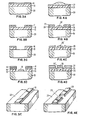
- FIGS. 1 and 2 The difficulty addressed by the present invention is illustrated in FIGS. 1 and 2.
- a resin glass layer, 14, is deposited onto an underlay surface, 12, it has a tendency to polymerize. If the underlay surface, 12, is made up of a compound which is a base, then the resin glass will polymerize in a three-dimensional mode, and as illustrated by layer 14 in FIG. 1, will result in localized thickness variations. Should a subsequent glass etching step be required using, for example, a reactive ion etch to uniformly remove the glass, the greater thicknesses of glass may not etch thoroughly. The resulting glass islands which remain, as illustrated in FIG. 2 at 14', can seriously affect subsequent processing and potentially destroy the utility of the resulting structure.
- non- etched glass examples include the interruption of a subsequently deposited layer where continuity or planarity of the layer is essential or resistance of the glass to an etching step intended to selectively remove the underlying layer, 12, whereby the glass inclusion "protects" that layer from the desired etching.
- FIGS. 3A-E and FIGS. 4A-E show the steps utilized in the above-cited patents to achieve the metal patterned film disclosed therein and illustrated in FIG. 3E.
- FIGS. 3A-E illustrate the ideal process and product embodiment as taught in patents 4,004,044 and 4,202,914.
- the glass polymerization problem discussed above can severely affect that process as illustrated in FIGS. 4A-4E.
- a glass resin layer deposited on a photoresist layer will undergo polymerization in a three-dimensional mode; and, it will not occur as the perfectly planar surface that is seen at 16 on FIG. 3A. Rather, the glass layer will have localized thickness variations as FIG. 4A illustrates at 26. It is possible that the glass thickness variations would not affect the further processing; however, if the glass inclusions are located in the path of the subsequent etching and metallization steps, they prove fatal to the patterned film. As illustrated in FIG. 4B, a uniform etching step, for example, a reactive ion etch of the resin glass, will not remove all of the glass from the photoresist layer in the critical area.
- the glass island, 26' which remains acts as a shield for the underlying photoresist, 25, in the etching step of 4C.
- the metal layer, 28, deposited in the step illustrated at 4D is deposited over the glass island 26' rather than directly on substrate 30. Consequently, the metal is lifted off with the glass in the following process step when the remaining photoresist, 25, is removed; thereby leaving the substrate bare.
- Void, 29, in perspective view 4E illustrates the point at which the metallization has been interrupted by an open resulting from the glass inclusion.
- the proposed solution herein involves a modification of the underlay surface itself. As herein disclosed, it has been determined that polymerization of glass resin occurs at the underlay surface and that the mode of the polymerization can be affected and effected by modification of the nature of the surface itself. If the underlay surface is made up of a material which is basic, the resin glass undergoes a three-dimensional polymerization. If, however, an acidic surface is induced, the polymerization of the resin glass layer is in a two-dimensional, linear mode.
- the underlay surface, 12, is a photoresist layer, for example, a novolak/diazo- quinone positive resist.
- the photoresist layer, 12, is comprised of an organic compound which is basic and which, upon direct resin glass deposition, by well-known spin on techniques, will induce a three-dimensional glass polymerization yielding the structure of FIG. 1.
- the inventive solution comprises modifying the photoresist underlay surface, 12, to render it acidic. This can be done by various alternative techniques, which would be obvious to one having ordinary skill in the art. However, in addition to rendering the surface acidic, the invention requires that there be no degradation of, nor change in the properties of the photoresist underlay.
- the photoresist surface is exposed to a short plasma ash in order to oxidize it and thereby render it acidic. Since only the surface of the photoresist comes into contact with the subsequently deposited resin glass, it is only the surface or the first monolayer of the photoresist that need be oxidized.
- Plasma ashing is a method, well-known and fully described in the literature, which is generally used for removing a photoresist layer (see US-A-4,202,914, Col. 4, lines 38 et seq.).
- the plasma ash is chosen for the ability of the excited oxygen atoms to quickly attack the top monolayer of the surface of the organic resist layer, form hydroxyl or carboxvl groups, and have no deleterious effect on the properties of the photoresist layer.
- the short ashing step provides the photoresist layer, 12, with an acidic surface monolayer, 13.
- the resin glass, 14, polymerizes linearly forming an evenly distributed layer free from the thickness variations attendant to the three-dimensional polymerization of the past.
Landscapes
- Engineering & Computer Science (AREA)
- Architecture (AREA)
- Structural Engineering (AREA)
- Physics & Mathematics (AREA)
- General Physics & Mathematics (AREA)
- Drying Of Semiconductors (AREA)
- Surface Treatment Of Glass (AREA)
- Photosensitive Polymer And Photoresist Processing (AREA)
Description
- The invention relates to a process for forming a lift-off glass mask on a substrate where the underlay surface is modified to control the glass polymerization.
- In the process of forming a glass lift-off mask on an underlay surface, the glass resin is often deposited over a photoresist made up of a solvent soluble polymer, specifically an organic layer. As the resin glass is spun onto the underlay surface, it has a tendency to polymerize. The polymerization occurs in a three-dimensional mode resulting in an unevenly distributed resin glass layer. If subsequent processing requires a step of etching the glass mask, the glass inclusions caused by the three-dimensional polymerization may not etch thoroughly and the glass which remains may present obstacles to subsequent processing, particularly if there is a need for a subsequently deposited layer to be planar and/or continuous. In the past, in order to eliminate the polymerization of glass resin, various extensive filtration techniques, such as filtering the glass through celite beds, have been utilized in efforts to "purify" the resin glass. Such attempts to prevent or modify the polymerization by treating the glass have proved unsuccessful; because, as herein disclosed, it has been determined that most of the polymerization takes place on the underlay surface itself, therefore requiring surface modification. Surface modification, in general, is not a new concept. Well-known teachings show surface modification to attain various ends, including increased adherence, better conductivity, improved dyeability and other ends (See: U.S. Patent 3,829,324 and discussions therein).
- From Patent Abstracts of Japan, Vol. 8, No. 181 (E-261) (1618) August 21, 1984 a method for forming a pattern using a multilayer resist is known wherein a first organic matter layer is formed on a silicon substrate and heated for thirty min. at 200°C. Subsequently, the layer is surface- treated in a plasma atmosphere using oxygen. The resulting silicon compound layer on the first organic matter layer is thermally treated and a resist pattern is formed on said layer. The resist pattern is transferred into the silicon compound layer and from there into the first organic matter layer. By this method the stability of the pattern formed through the multilayer resist is improved.
- It is an objective of the present invention to provide a process for forming a lift-off glass mask where the underlay surface is modified in order to control the polymerization of subsequently deposited resin glass.
- The object of the invention is achieved by a process according to claim 1.
- According to the invention an evenly distributed glass overlay surface is obtained and thus metal opens in glass lift-off/metallization processing are avoided. The method by which these objectives are attained teaches modification of the underlay surface onto which a resin glass layer is to be deposited. By modification of the underlying surface, to render it acidic rather than basic, the mode of the polymerization which takes place in the deposited glass is altered from a three-dimensional to a two-dimensional mode insuring even distribution of the resin glass layer.
- FIG. 1 is a cross-sectional view of an unevenly distributed resin glass layer formed on an underlay surface in accordance with well-known techniques.
- FIG. 2 illustrates the problem of residual glass deposits left after a glass etching step.
- FIGS. 3A-3D are cross-sectional views of the ideal metallization/lift-off technique known in the art.
- FIG. 3E is a perspective view of same.
- FIGS. 4A-4D are cross-sectional views of the actual metallization/lift-off processes known in the art.
- FIG. 4E is a perspective view of the same.
- FIG. 5 is a cross-sectional view illustrating the inventive modification to the underlay surface.
- FIG. 6 is a cross-sectional view of an evenly distributed resin glass layer deposited after applying the subject inventive method.
- The difficulty addressed by the present invention is illustrated in FIGS. 1 and 2. When a resin glass layer, 14, is deposited onto an underlay surface, 12, it has a tendency to polymerize. If the underlay surface, 12, is made up of a compound which is a base, then the resin glass will polymerize in a three-dimensional mode, and as illustrated by
layer 14 in FIG. 1, will result in localized thickness variations. Should a subsequent glass etching step be required using, for example, a reactive ion etch to uniformly remove the glass, the greater thicknesses of glass may not etch thoroughly. The resulting glass islands which remain, as illustrated in FIG. 2 at 14', can seriously affect subsequent processing and potentially destroy the utility of the resulting structure. Examples of the problems that the non- etched glass may present include the interruption of a subsequently deposited layer where continuity or planarity of the layer is essential or resistance of the glass to an etching step intended to selectively remove the underlying layer, 12, whereby the glass inclusion "protects" that layer from the desired etching. - More specifically, the effect of the subject polymerization on the formation of metal patterned films utilizing transparent lift-off masks, as disclosed in U.S. Patents 4,004,044 and 4,202,914, is illustrated in FIGS. 3A-E and FIGS. 4A-E. FIGS. 3A-3D show the steps utilized in the above-cited patents to achieve the metal patterned film disclosed therein and illustrated in FIG. 3E. The steps involved are: A) depositing a
photoresist layer 15, on a substrate, 20 and overlying said photoresist with a glass lift-off mask layer, 16; B) etching said lift-off mask, 16 by the use of an additional photoresist layer 17: C) removing thephotoresist layers metal layer 18; E) removing theremaining photoresist 15 and thereby removing the overlying metal andglass layers - A glass resin layer deposited on a photoresist layer will undergo polymerization in a three-dimensional mode; and, it will not occur as the perfectly planar surface that is seen at 16 on FIG. 3A. Rather, the glass layer will have localized thickness variations as FIG. 4A illustrates at 26. It is possible that the glass thickness variations would not affect the further processing; however, if the glass inclusions are located in the path of the subsequent etching and metallization steps, they prove fatal to the patterned film. As illustrated in FIG. 4B, a uniform etching step, for example, a reactive ion etch of the resin glass, will not remove all of the glass from the photoresist layer in the critical area. The glass island, 26', which remains acts as a shield for the underlying photoresist, 25, in the etching step of 4C. The metal layer, 28, deposited in the step illustrated at 4D is deposited over the glass island 26' rather than directly on
substrate 30. Consequently, the metal is lifted off with the glass in the following process step when the remaining photoresist, 25, is removed; thereby leaving the substrate bare. Void, 29, in perspective view 4E illustrates the point at which the metallization has been interrupted by an open resulting from the glass inclusion. - Efforts to address this problem in the past, as noted above, concentrated on the resin glass, usually between 60% and 80% silicon dioxide, Si02, and 40% to 20% carbon, hydrogen and silicon molecules, using filtration techniques to "purify" and regulate the resin glass to be deposited. The proposed solution herein involves a modification of the underlay surface itself. As herein disclosed, it has been determined that polymerization of glass resin occurs at the underlay surface and that the mode of the polymerization can be affected and effected by modification of the nature of the surface itself. If the underlay surface is made up of a material which is basic, the resin glass undergoes a three-dimensional polymerization. If, however, an acidic surface is induced, the polymerization of the resin glass layer is in a two-dimensional, linear mode.
- In the preferred embodiment herein, as illustrated in FIG. 5, the underlay surface, 12, is a photoresist layer, for example, a novolak/diazo- quinone positive resist. The photoresist layer, 12, is comprised of an organic compound which is basic and which, upon direct resin glass deposition, by well-known spin on techniques, will induce a three-dimensional glass polymerization yielding the structure of FIG. 1. The inventive solution comprises modifying the photoresist underlay surface, 12, to render it acidic. This can be done by various alternative techniques, which would be obvious to one having ordinary skill in the art. However, in addition to rendering the surface acidic, the invention requires that there be no degradation of, nor change in the properties of the photoresist underlay. Therefore, in the preferred embodiment, the photoresist surface is exposed to a short plasma ash in order to oxidize it and thereby render it acidic. Since only the surface of the photoresist comes into contact with the subsequently deposited resin glass, it is only the surface or the first monolayer of the photoresist that need be oxidized. Plasma ashing is a method, well-known and fully described in the literature, which is generally used for removing a photoresist layer (see US-A-4,202,914, Col. 4, lines 38 et seq.). The plasma ashing step performed, therefore, must be of very short duration, for example 15-20 seconds, in order to induce the acidic surface without removing the photoresist. Furthermore, the plasma ash is chosen for the ability of the excited oxygen atoms to quickly attack the top monolayer of the surface of the organic resist layer, form hydroxyl or carboxvl groups, and have no deleterious effect on the properties of the photoresist layer. As illustrated in FIG. 5, the short ashing step provides the photoresist layer, 12, with an acidic surface monolayer, 13. When a resin glass layer is subsequently deposited over the acidic top surface monolayer, as illustrated in FIG. 6, the resin glass, 14, polymerizes linearly forming an evenly distributed layer free from the thickness variations attendant to the three-dimensional polymerization of the past.
Claims (5)
characterized in that
Applications Claiming Priority (2)
| Application Number | Priority Date | Filing Date | Title |
|---|---|---|---|
| US62487884A | 1984-06-27 | 1984-06-27 | |
| US624878 | 1990-12-05 |
Publications (3)
| Publication Number | Publication Date |
|---|---|
| EP0166307A2 EP0166307A2 (en) | 1986-01-02 |
| EP0166307A3 EP0166307A3 (en) | 1987-07-29 |
| EP0166307B1 true EP0166307B1 (en) | 1990-02-28 |
Family
ID=24503711
Family Applications (1)
| Application Number | Title | Priority Date | Filing Date |
|---|---|---|---|
| EP19850107250 Expired EP0166307B1 (en) | 1984-06-27 | 1985-06-14 | Process for forming a lift-off glass mask on a substrate |
Country Status (3)
| Country | Link |
|---|---|
| EP (1) | EP0166307B1 (en) |
| JP (1) | JPS6113628A (en) |
| DE (1) | DE3576222D1 (en) |
Family Cites Families (3)
| Publication number | Priority date | Publication date | Assignee | Title |
|---|---|---|---|---|
| DE2526662B2 (en) * | 1975-06-14 | 1979-09-13 | Motoren- Und Turbinen-Union Friedrichshafen Gmbh, 7990 Friedrichshafen | Transmission linkage between a centrifugal governor and a fuel metering device of an internal combustion engine |
| JPS5749233A (en) * | 1980-09-08 | 1982-03-23 | Mitsubishi Electric Corp | Laminar structure resist and forming method for pattern thereof |
| CA1188251A (en) * | 1981-10-07 | 1985-06-04 | Joel L. Williams | Substrate with chemically modified surface and method of manufacture thereof |
-
1985
- 1985-03-15 JP JP5073585A patent/JPS6113628A/en active Granted
- 1985-06-14 DE DE8585107250T patent/DE3576222D1/en not_active Expired - Lifetime
- 1985-06-14 EP EP19850107250 patent/EP0166307B1/en not_active Expired
Also Published As
| Publication number | Publication date |
|---|---|
| EP0166307A3 (en) | 1987-07-29 |
| JPH0562815B2 (en) | 1993-09-09 |
| JPS6113628A (en) | 1986-01-21 |
| DE3576222D1 (en) | 1990-04-05 |
| EP0166307A2 (en) | 1986-01-02 |
Similar Documents
| Publication | Publication Date | Title |
|---|---|---|
| CA1123118A (en) | Fabrication of integrated circuits utilizing thick high-resolution patterns | |
| EP0238690B1 (en) | Process for forming sidewalls | |
| US4497684A (en) | Lift-off process for depositing metal on a substrate | |
| US5277749A (en) | Methods and apparatus for relieving stress and resisting stencil delamination when performing lift-off processes that utilize high stress metals and/or multiple evaporation steps | |
| EP0043458B1 (en) | Process for forming a metallurgy interconnection system | |
| CA1192480A (en) | Adhesion bond-breaking of lift-off regions on semiconductor structures | |
| CA1155736A (en) | Method of etching polyimide | |
| KR20010050906A (en) | A method of processing specimens, an apparatus therefor and a method of manufacture of a magnetic head | |
| JPS5812344B2 (en) | Method for forming metal patterns using copper as a base material | |
| US3705055A (en) | Method of descumming photoresist patterns | |
| EP1089113A2 (en) | Transfer body and method using the same | |
| US5503961A (en) | Process for forming multilayer lift-off structures | |
| JPH02218010A (en) | Manufacture of thin film magnetic recording head | |
| EP0132585B1 (en) | Lift-off process and composition therefor | |
| US5269890A (en) | Electrochemical process and product therefrom | |
| US4601913A (en) | Underlay surface modification to control resin glass polymerization | |
| EP0166307A2 (en) | Process for forming a lift-off glass mask on a substrate | |
| KR100407601B1 (en) | Method for forming micro pattern in thermoset polymer film by using thermal treatment and capillary force | |
| EP0200477A2 (en) | Process for pattern formation | |
| JPS646449B2 (en) | ||
| KR960013140B1 (en) | Manufacturing Method of Semiconductor Device | |
| JPH0339340B2 (en) | ||
| KR950004974B1 (en) | Fine pattern formation method | |
| KR0186018B1 (en) | How to remove photoresist and polymer | |
| JPH0470626B2 (en) |
Legal Events
| Date | Code | Title | Description |
|---|---|---|---|
| PUAI | Public reference made under article 153(3) epc to a published international application that has entered the european phase |
Free format text: ORIGINAL CODE: 0009012 |
|
| AK | Designated contracting states |
Designated state(s): DE FR GB |
|
| 17P | Request for examination filed |
Effective date: 19860424 |
|
| PUAL | Search report despatched |
Free format text: ORIGINAL CODE: 0009013 |
|
| AK | Designated contracting states |
Kind code of ref document: A3 Designated state(s): DE FR GB |
|
| 17Q | First examination report despatched |
Effective date: 19881102 |
|
| GRAA | (expected) grant |
Free format text: ORIGINAL CODE: 0009210 |
|
| AK | Designated contracting states |
Kind code of ref document: B1 Designated state(s): DE FR GB |
|
| REF | Corresponds to: |
Ref document number: 3576222 Country of ref document: DE Date of ref document: 19900405 |
|
| ET | Fr: translation filed | ||
| PLBE | No opposition filed within time limit |
Free format text: ORIGINAL CODE: 0009261 |
|
| STAA | Information on the status of an ep patent application or granted ep patent |
Free format text: STATUS: NO OPPOSITION FILED WITHIN TIME LIMIT |
|
| 26N | No opposition filed | ||
| PGFP | Annual fee paid to national office [announced via postgrant information from national office to epo] |
Ref country code: GB Payment date: 19920507 Year of fee payment: 8 |
|
| PGFP | Annual fee paid to national office [announced via postgrant information from national office to epo] |
Ref country code: FR Payment date: 19920601 Year of fee payment: 8 |
|
| PGFP | Annual fee paid to national office [announced via postgrant information from national office to epo] |
Ref country code: DE Payment date: 19920619 Year of fee payment: 8 |
|
| PG25 | Lapsed in a contracting state [announced via postgrant information from national office to epo] |
Ref country code: GB Effective date: 19930614 |
|
| GBPC | Gb: european patent ceased through non-payment of renewal fee |
Effective date: 19930614 |
|
| PG25 | Lapsed in a contracting state [announced via postgrant information from national office to epo] |
Ref country code: FR Effective date: 19940228 |
|
| PG25 | Lapsed in a contracting state [announced via postgrant information from national office to epo] |
Ref country code: DE Effective date: 19940301 |
|
| REG | Reference to a national code |
Ref country code: FR Ref legal event code: ST |