EP0166141A2 - Method of forming dielectric isolation - Google Patents
Method of forming dielectric isolation Download PDFInfo
- Publication number
- EP0166141A2 EP0166141A2 EP85105717A EP85105717A EP0166141A2 EP 0166141 A2 EP0166141 A2 EP 0166141A2 EP 85105717 A EP85105717 A EP 85105717A EP 85105717 A EP85105717 A EP 85105717A EP 0166141 A2 EP0166141 A2 EP 0166141A2
- Authority
- EP
- European Patent Office
- Prior art keywords
- layer
- trench
- insulating layer
- passivating
- forming
- Prior art date
- Legal status (The legal status is an assumption and is not a legal conclusion. Google has not performed a legal analysis and makes no representation as to the accuracy of the status listed.)
- Granted
Links
- 238000000034 method Methods 0.000 title claims abstract description 26
- 238000002955 isolation Methods 0.000 title claims abstract description 23
- VYPSYNLAJGMNEJ-UHFFFAOYSA-N Silicium dioxide Chemical compound O=[Si]=O VYPSYNLAJGMNEJ-UHFFFAOYSA-N 0.000 claims abstract description 53
- 239000000758 substrate Substances 0.000 claims abstract description 51
- 235000012239 silicon dioxide Nutrition 0.000 claims abstract description 27
- 239000000377 silicon dioxide Substances 0.000 claims abstract description 26
- 239000004642 Polyimide Substances 0.000 claims abstract description 24
- 229920001721 polyimide Polymers 0.000 claims abstract description 24
- 229910052581 Si3N4 Inorganic materials 0.000 claims abstract description 22
- HQVNEWCFYHHQES-UHFFFAOYSA-N silicon nitride Chemical compound N12[Si]34N5[Si]62N3[Si]51N64 HQVNEWCFYHHQES-UHFFFAOYSA-N 0.000 claims abstract description 22
- XUIMIQQOPSSXEZ-UHFFFAOYSA-N Silicon Chemical compound [Si] XUIMIQQOPSSXEZ-UHFFFAOYSA-N 0.000 claims abstract description 13
- 229910052710 silicon Inorganic materials 0.000 claims abstract description 13
- 239000010703 silicon Substances 0.000 claims abstract description 13
- 238000002161 passivation Methods 0.000 claims abstract description 12
- 239000004065 semiconductor Substances 0.000 claims abstract description 11
- 238000005530 etching Methods 0.000 claims description 24
- 239000003989 dielectric material Substances 0.000 claims description 9
- ZXEYZECDXFPJRJ-UHFFFAOYSA-N $l^{3}-silane;platinum Chemical compound [SiH3].[Pt] ZXEYZECDXFPJRJ-UHFFFAOYSA-N 0.000 claims description 6
- 230000015572 biosynthetic process Effects 0.000 claims description 6
- 238000011049 filling Methods 0.000 claims description 5
- 229910021339 platinum silicide Inorganic materials 0.000 claims description 5
- 239000000463 material Substances 0.000 claims description 4
- 238000000151 deposition Methods 0.000 claims description 3
- 239000011248 coating agent Substances 0.000 claims description 2
- 238000000576 coating method Methods 0.000 claims description 2
- 239000010410 layer Substances 0.000 description 55
- 150000004767 nitrides Chemical class 0.000 description 10
- 238000001020 plasma etching Methods 0.000 description 7
- 150000002500 ions Chemical class 0.000 description 3
- 238000001465 metallisation Methods 0.000 description 3
- -1 14 and 14' Chemical compound 0.000 description 2
- YCIMNLLNPGFGHC-UHFFFAOYSA-N catechol Chemical compound OC1=CC=CC=C1O YCIMNLLNPGFGHC-UHFFFAOYSA-N 0.000 description 2
- 238000005229 chemical vapour deposition Methods 0.000 description 2
- 238000004140 cleaning Methods 0.000 description 2
- 238000011109 contamination Methods 0.000 description 2
- 230000008021 deposition Effects 0.000 description 2
- 238000001514 detection method Methods 0.000 description 2
- 238000009413 insulation Methods 0.000 description 2
- 239000012212 insulator Substances 0.000 description 2
- 238000004518 low pressure chemical vapour deposition Methods 0.000 description 2
- 230000003647 oxidation Effects 0.000 description 2
- 238000007254 oxidation reaction Methods 0.000 description 2
- XPDWGBQVDMORPB-UHFFFAOYSA-N Fluoroform Chemical compound FC(F)F XPDWGBQVDMORPB-UHFFFAOYSA-N 0.000 description 1
- DGAQECJNVWCQMB-PUAWFVPOSA-M Ilexoside XXIX Chemical compound C[C@@H]1CC[C@@]2(CC[C@@]3(C(=CC[C@H]4[C@]3(CC[C@@H]5[C@@]4(CC[C@@H](C5(C)C)OS(=O)(=O)[O-])C)C)[C@@H]2[C@]1(C)O)C)C(=O)O[C@H]6[C@@H]([C@H]([C@@H]([C@H](O6)CO)O)O)O.[Na+] DGAQECJNVWCQMB-PUAWFVPOSA-M 0.000 description 1
- 239000002253 acid Substances 0.000 description 1
- 239000007795 chemical reaction product Substances 0.000 description 1
- 239000004020 conductor Substances 0.000 description 1
- 238000009792 diffusion process Methods 0.000 description 1
- 230000000694 effects Effects 0.000 description 1
- 230000003993 interaction Effects 0.000 description 1
- 238000004519 manufacturing process Methods 0.000 description 1
- 229910052751 metal Inorganic materials 0.000 description 1
- 239000002184 metal Substances 0.000 description 1
- 230000001590 oxidative effect Effects 0.000 description 1
- 238000002360 preparation method Methods 0.000 description 1
- 239000011241 protective layer Substances 0.000 description 1
- 239000010453 quartz Substances 0.000 description 1
- 229910052708 sodium Inorganic materials 0.000 description 1
- 239000011734 sodium Substances 0.000 description 1
Images


Classifications
-
- H—ELECTRICITY
- H01—ELECTRIC ELEMENTS
- H01L—SEMICONDUCTOR DEVICES NOT COVERED BY CLASS H10
- H01L21/00—Processes or apparatus adapted for the manufacture or treatment of semiconductor or solid state devices or of parts thereof
- H01L21/70—Manufacture or treatment of devices consisting of a plurality of solid state components formed in or on a common substrate or of parts thereof; Manufacture of integrated circuit devices or of parts thereof
- H01L21/71—Manufacture of specific parts of devices defined in group H01L21/70
- H01L21/76—Making of isolation regions between components
- H01L21/762—Dielectric regions, e.g. EPIC dielectric isolation, LOCOS; Trench refilling techniques, SOI technology, use of channel stoppers
- H01L21/76224—Dielectric regions, e.g. EPIC dielectric isolation, LOCOS; Trench refilling techniques, SOI technology, use of channel stoppers using trench refilling with dielectric materials
- H01L21/76232—Dielectric regions, e.g. EPIC dielectric isolation, LOCOS; Trench refilling techniques, SOI technology, use of channel stoppers using trench refilling with dielectric materials of trenches having a shape other than rectangular or V-shape, e.g. rounded corners, oblique or rounded trench walls
-
- H—ELECTRICITY
- H01—ELECTRIC ELEMENTS
- H01L—SEMICONDUCTOR DEVICES NOT COVERED BY CLASS H10
- H01L21/00—Processes or apparatus adapted for the manufacture or treatment of semiconductor or solid state devices or of parts thereof
- H01L21/02—Manufacture or treatment of semiconductor devices or of parts thereof
- H01L21/04—Manufacture or treatment of semiconductor devices or of parts thereof the devices having potential barriers, e.g. a PN junction, depletion layer or carrier concentration layer
- H01L21/18—Manufacture or treatment of semiconductor devices or of parts thereof the devices having potential barriers, e.g. a PN junction, depletion layer or carrier concentration layer the devices having semiconductor bodies comprising elements of Group IV of the Periodic Table or AIIIBV compounds with or without impurities, e.g. doping materials
- H01L21/28—Manufacture of electrodes on semiconductor bodies using processes or apparatus not provided for in groups H01L21/20 - H01L21/268
-
- H—ELECTRICITY
- H01—ELECTRIC ELEMENTS
- H01L—SEMICONDUCTOR DEVICES NOT COVERED BY CLASS H10
- H01L21/00—Processes or apparatus adapted for the manufacture or treatment of semiconductor or solid state devices or of parts thereof
- H01L21/70—Manufacture or treatment of devices consisting of a plurality of solid state components formed in or on a common substrate or of parts thereof; Manufacture of integrated circuit devices or of parts thereof
- H01L21/71—Manufacture of specific parts of devices defined in group H01L21/70
- H01L21/74—Making of localized buried regions, e.g. buried collector layers, internal connections substrate contacts
- H01L21/743—Making of internal connections, substrate contacts
-
- H—ELECTRICITY
- H01—ELECTRIC ELEMENTS
- H01L—SEMICONDUCTOR DEVICES NOT COVERED BY CLASS H10
- H01L21/00—Processes or apparatus adapted for the manufacture or treatment of semiconductor or solid state devices or of parts thereof
- H01L21/70—Manufacture or treatment of devices consisting of a plurality of solid state components formed in or on a common substrate or of parts thereof; Manufacture of integrated circuit devices or of parts thereof
- H01L21/71—Manufacture of specific parts of devices defined in group H01L21/70
- H01L21/768—Applying interconnections to be used for carrying current between separate components within a device comprising conductors and dielectrics
- H01L21/76801—Applying interconnections to be used for carrying current between separate components within a device comprising conductors and dielectrics characterised by the formation and the after-treatment of the dielectrics, e.g. smoothing
- H01L21/76802—Applying interconnections to be used for carrying current between separate components within a device comprising conductors and dielectrics characterised by the formation and the after-treatment of the dielectrics, e.g. smoothing by forming openings in dielectrics
Definitions
- the invention relates to a method of forming dielectric isolation for an integrated circuit structure in a semiconductor substrate comprising the steps of forming at least one trench having substantially vertical sidewalls and at least one contact in said substrate by etching while using a suitable mask pattern, and filling said trench with dielectric material.
- isolation In the formation of high density integrated circuits, there is a need to isolate the components from one another in order to prevent undesired interactions.
- One means of achieving isolation is to etch a series or pattern of isolation trenches in the semiconductor substrate, passivate them with oxide and nitride and then fill them with a dielectric material.
- the typical processing consists of finishing all high- temperature processing including formation of emitter contacts and emitter diffusion prior to the formation of the isolation trenches.
- the dielectric material is deposited over the entire patterned substrate so as to overfill the trenches.
- the dielectric material is then etched back to re-expose the substrate and contacts, leaving the trenches "full".
- the dielectric material is generally over-etched below the recess level, thus leaving a significant step at the trench peripheries. This topographical non-planarity has been found to create discontinuities in the subsequently formed metallization line patterns.
- a further well-known difficulty with regard to the isolation trenches is in the continuous nitride passivation of the substrate, especially at the trench peripheries.
- the top substrate surface is passivated with the nitride before trench etching; the trench sidewalls are then passivated with a subsequent separate nitride deposition.
- the protection of the underlying commonly used oxide insulator is relatively poor.
- the result of the poor nitride passivation can include: silicon- to-metal shorts near the top edge of the trenches as a consequence of accidental removal of the oxide insulator in a cleaning or etching step that follows; or contamination of the insulating layer with, for example, sodium from a subsequently deposited quartz layer.
- the subject invention which provides, in a silicon substrate having an etched isolation trench pattern, for an undercut silicon dioxide insulation layer and a recessed silicon sidewall arrangement below protective layers of silicon nitride at the trench peripheries.
- the invention further teaches the establishment, through previously deposited layers, of a polyimide etchback end detection point, above the level of the recessed contacts in the silicon substrate, in order to attain a higher degree of planarity between the polyimide filling and the upper substrate surface.
- FIG. 1 The problems to be rectified by the subject invention are illustrated in FIG. 1.
- successive layers of silicon dioxide 16 and silicon nitride 14 are deposited on a silicon substrate having an integrated circuit structure formed therein.
- a pattern of isolation trenches is then etched into the substrate using an appropriate mask.
- the trench next undergoes an oxidation step (i.e. is exposed to an oxidizing atmosphere) to form a layer, 13, of silicon dioxide; this is followed by successive chemical vapor deposition of another layer 12 of silicon dioxide and, a passivation layer of silicon nitride, 15, in the trench 18.
- the nitride layer, 15, and oxide layers 12 and 13 are next successively subjected to vertically directional reactive ion etching.
- the second problem to be resolved arises after the "passivated" trench is filled with the dielectric material, such as polyimide.
- the polyimide, 22 in FIG. 1 is deposited in sufficient quantity to overfill the trench 18; this leaves an excess layer of polyimide on the substrate surface.
- the excess polyimide is then etched away from the substrate in order to re-expose the contacts, 11.
- the result of the polyimide etching step is an over-etching of the polyimide in the trench to the level of the recessed contacts which is below the level of the surrounding substrate.
- the resulting steps, 19, between the substrate and the polyimide at the trench peripheries present difficulties in achieving unbroken metallization line patterns in subsequent processing steps.
- the present invention proposes a series of method steps and the resulting structures which alleviate both the insufficient passivation and the non-planarity problems associated with the isolation trench structures of the prior art.
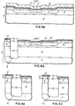
- FIG. 2A is an illustration of the poorly passivated trench periphery, 25A, resulting from well known processing steps.
- FIG. 2B illustrates, the inventive structural solution arrived at by utilizing the subject inventive method. There can be seen, in FIG. 2B, a continuous layer of silicon nitride, 14B, at the dielectric isolation trench periphery, 25B.
- FIGS. 3-6 describe the invention as it arrives at the solution illustrated in FIG. 2B.
- the invention is described with reference to the preferred embodiment and should not be read to exclude appropriate alternative materials or processes.
- the invention lies in the process steps, and structure therefrom, directly related to the formation of the isolation trenches themselves; and, does not include the steps related to the preparation of the substrate or the formation of the integrated circuit structure therein in arriving at the structure found in FIG. 3A.
- the invention also does not include the personalization processes subsequent to the deposition and etching of nitride layer 29 of FIG. 9.
- FIG. 3A shows a substrate, 17, having an integrated circuit structure formed therein.
- a layer, 16, of silicon dioxide has been deposited over the substrate and a passivating layer, 14, of silicon nitride deposited over that silicon dioxide layer in accordance with teachings well-known in the art.
- Layer 16' depicts an oxide layer which has been grown thermally in the emitter contact region, 11, during drive-in of the N + emitter.
- a silicon nitride layer 14' is deposited, preferably through low pressure chemical vapor deposition. This is followed by plasma-aided chemical vapor deposition of a thick oxide layer, 32.
- a trench, 18, needed for dielectric isolation is formed, as illustrated in FIG.
- the oxide layer, 32 by photolithographically etching the oxide layer, 32 and then using the patterned oxide as a mask for etching the silicon nitride layers 14 and 14', silicon dioxide layer, 16, and the silicon substrate.
- a multi-layer resist mask bearing the pattern desired for the isolation scheme and for the isolation contact regions, is formed over the prepared substrate and the oxide 32 is etched using reactive ion etching through the mask.
- the silicon nitride, 14 and 14', and silicon dioxide, 16, layers can be etched by CF 4 , for example, and the silicon by an SF 6 reactive ion etchant. The results, as shown in FIG.
- etchants used and the steps for controlling the width, depth and shape of the trench are variables well-known in the art and can be selected in response to the specific needs of the ultimate endproduct.
- a selective anisotropic etchant pyrocatechol for example, is used to laterally etch only the silicon of substrate 17 and thereby expand the sidewalls of trench 18.
- the trench, 18, has an opening 28 which has lateral dimensions corresponding to those of openings 24 and 26.
- FIG. 4B illustrates the lateral expansion to 28' such that the trench sidewalls 0 are now recessed by approximately 2000 A relative to the silicon nitride, 14 and 14', and silicon dioxide, 16, layers.
- a further etching step is then performed using a selective isotropic etchant, such as buffered HF acid, to etch only the silicon dioxide layer 16.
- the isotropic etchant etches in "all" directions.
- the result achieved, as illustrated in FIG. 4C, is an expansion of opening 26 to 26' (also by approximately 2000 A,) leaving the layer, 16, of silicon dioxide recessed or undercut, relative to the silicon nitride layers, 14 and 14' above.
- the p-contacts may now be formed in accordance with well known procedures.
- a layer of silicon dioxide, 20, is then formed at all exposed silicon surfaces by thermal oxidation, illustrated in FIG. 5. The entire surface is next coated with a passivation layer, 15, of silicon nitride.
- the etch back to expose the platinum silicide, 30, for contacts, 11, will overetch the polyimide from the level of the upper surface of nitride layer 14 on the coated substrate down to the level of the recessed platinum silicide in the contact regions and yield a large step as illustrated in FIG. 1.
- a relatively thick layer, 21, of silicon dioxide is conformally deposited over the entire surface of the substrate, as shown in FIG. 7, using for, example, low pressure chemical vapor deposition.
- the thickness of the silicon dioxide layer, 21, is controlled such that the level of the upper surface, level 31, of the layer in the contact, 11, region is above the upper surface of layer 14 in the non-contact, non-trench region (i.e. above the uppermost surface of the coated substrate field).
- the level of the silicon dioxide layer, 21, in the contact region is the level at which the subsequent polyimide etchback will stop.
- Polyimide, 22, is then deposited so as to overfill the trench, leaving an excess layer of polyimide on the silicon dioxide layer, 21, in the non-trench regions. The excess polyimide is then etched away, using a standard selective etchant, to the etch end-point, level 31, of the upper surface of silicon dioxide layer, 21, in the contact region, see FIG. 8.
- the silicon dioxide layer, 21, is next removed in all of the non-trench regions using vertically directional reactive ion etch, such as a cHF 3 reactive ion etch, in order to expose the platinum silicide, 30, in the non-trench contact regions.
- vertically directional reactive ion etch such as a cHF 3 reactive ion etch
- the result, as seen in FIG. 9, is a substantially planar semiconductor configuration having a polyimide filled isolation trench.
- the silicon dioxide, 21, in the trench is not affected by the etching step other than a slight etch at the top of the trench.
- the presence of the silicon dioxide, 21, in the trench also does not affect the trench isolation characteristics.
- a final layer, 29, of silicon nitride may be deposited and etched through reactive ion etching leaving only a small layer on the trench peripheries contributing further to both the passivation and planarity of the configuration.
- the substrate semiconductor structure is subjected to subsequent metallization/personalization, 23, processing.
Landscapes
- Engineering & Computer Science (AREA)
- Physics & Mathematics (AREA)
- Condensed Matter Physics & Semiconductors (AREA)
- General Physics & Mathematics (AREA)
- Manufacturing & Machinery (AREA)
- Computer Hardware Design (AREA)
- Microelectronics & Electronic Packaging (AREA)
- Power Engineering (AREA)
- Element Separation (AREA)
- Semiconductor Memories (AREA)
Abstract
Description
- The invention relates to a method of forming dielectric isolation for an integrated circuit structure in a semiconductor substrate comprising the steps of forming at least one trench having substantially vertical sidewalls and at least one contact in said substrate by etching while using a suitable mask pattern, and filling said trench with dielectric material.
- In the formation of high density integrated circuits, there is a need to isolate the components from one another in order to prevent undesired interactions. One means of achieving isolation, in the art, is to etch a series or pattern of isolation trenches in the semiconductor substrate, passivate them with oxide and nitride and then fill them with a dielectric material. When a dielectric material such as polyimide is used, the typical processing consists of finishing all high- temperature processing including formation of emitter contacts and emitter diffusion prior to the formation of the isolation trenches. In filling the trenches, the dielectric material is deposited over the entire patterned substrate so as to overfill the trenches. The dielectric material is then etched back to re-expose the substrate and contacts, leaving the trenches "full". In order, however, to guarantee exposure of the contacts, which are located in recesses in the substrate surface, the dielectric material is generally over-etched below the recess level, thus leaving a significant step at the trench peripheries. This topographical non-planarity has been found to create discontinuities in the subsequently formed metallization line patterns.
- A further well-known difficulty with regard to the isolation trenches is in the continuous nitride passivation of the substrate, especially at the trench peripheries. In a typical process, the top substrate surface is passivated with the nitride before trench etching; the trench sidewalls are then passivated with a subsequent separate nitride deposition. As such, at the edge, the protection of the underlying commonly used oxide insulator is relatively poor. The result of the poor nitride passivation can include: silicon- to-metal shorts near the top edge of the trenches as a consequence of accidental removal of the oxide insulator in a cleaning or etching step that follows; or contamination of the insulating layer with, for example, sodium from a subsequently deposited quartz layer.
- It is therefore an objective of the present invention to provide an improved isolation trench scheme.
- It is another objective of the invention to provide a unique isolation trench configuration having improved insulation and passivation characteristics.
- It is still another objective of the invention to provide an undercut insulating layer at the top of an isolation trench, and an overlying passivation layer at the top of and coating all of the trench in order to avoid the effects of poor passivation.
- It is a further objective of the invention to provide a high degree of planarity in an isolation trench/ substrate structure.
- Finally, it is an objective of the invention to provide for a polyimide etchback end-detection point which is above the level of recessed substrate contacts and above the level of the upper substrate surface allowing for a planar surface along the polyimide filled trenches and the substrate.
- These and other objectives are accomplished by the subject invention which provides, in a silicon substrate having an etched isolation trench pattern, for an undercut silicon dioxide insulation layer and a recessed silicon sidewall arrangement below protective layers of silicon nitride at the trench peripheries. The invention further teaches the establishment, through previously deposited layers, of a polyimide etchback end detection point, above the level of the recessed contacts in the silicon substrate, in order to attain a higher degree of planarity between the polyimide filling and the upper substrate surface.
- One way of carrying out the invention is described in detail below with reference to drawings in which:
- FIG. 1 is a cross-sectional view of a semiconductor substrate structure produced in accordance with well-known fabrication processes.
- FIGS. 2A illustrate a cross-sectional view of and 2B an isolation trench periphery produced under (A) the old and (B) the new methods.
- FIGS. 3A are cross-sectional views of the semi-and 3B conductor substrate prior to applying the subject method.
- FIGS. 4A, are cross-sectional views of an isola-4B and 4C tion trench illustrating the etching steps necessary to achieve the subject invention.
- FIGS. 5, 6, are cross-sectional views illustrating 7, 8 and 9 process steps and the resulting struc- turps in accordance with the subject invention.
- FIG. 10 is a cross-sectional view of the inventive structure undergoing further processing.
- The problems to be rectified by the subject invention are illustrated in FIG. 1. In a typical process successive layers of
silicon dioxide 16 andsilicon nitride 14 are deposited on a silicon substrate having an integrated circuit structure formed therein. A pattern of isolation trenches, is then etched into the substrate using an appropriate mask. The trench next undergoes an oxidation step (i.e. is exposed to an oxidizing atmosphere) to form a layer, 13, of silicon dioxide; this is followed by successive chemical vapor deposition ofanother layer 12 of silicon dioxide and, a passivation layer of silicon nitride, 15, in thetrench 18. The nitride layer, 15, andoxide layers silicon nitride layers - The second problem to be resolved arises after the "passivated" trench is filled with the dielectric material, such as polyimide. The polyimide, 22 in FIG. 1, is deposited in sufficient quantity to overfill the
trench 18; this leaves an excess layer of polyimide on the substrate surface. The excess polyimide is then etched away from the substrate in order to re-expose the contacts, 11. The result of the polyimide etching step is an over-etching of the polyimide in the trench to the level of the recessed contacts which is below the level of the surrounding substrate. The resulting steps, 19, between the substrate and the polyimide at the trench peripheries present difficulties in achieving unbroken metallization line patterns in subsequent processing steps. - The present invention proposes a series of method steps and the resulting structures which alleviate both the insufficient passivation and the non-planarity problems associated with the isolation trench structures of the prior art.
- FIG. 2A is an illustration of the poorly passivated trench periphery, 25A, resulting from well known processing steps. FIG. 2B illustrates, the inventive structural solution arrived at by utilizing the subject inventive method. There can be seen, in FIG. 2B, a continuous layer of silicon nitride, 14B, at the dielectric isolation trench periphery, 25B. The teachings that follow, with reference to FIGS. 3-6, describe the invention as it arrives at the solution illustrated in FIG. 2B. The invention is described with reference to the preferred embodiment and should not be read to exclude appropriate alternative materials or processes. The invention lies in the process steps, and structure therefrom, directly related to the formation of the isolation trenches themselves; and, does not include the steps related to the preparation of the substrate or the formation of the integrated circuit structure therein in arriving at the structure found in FIG. 3A. The invention also does not include the personalization processes subsequent to the deposition and etching of
nitride layer 29 of FIG. 9. - FIG. 3A shows a substrate, 17, having an integrated circuit structure formed therein. A layer, 16, of silicon dioxide has been deposited over the substrate and a passivating layer, 14, of silicon nitride deposited over that silicon dioxide layer in accordance with teachings well-known in the art. Layer 16' depicts an oxide layer which has been grown thermally in the emitter contact region, 11, during drive-in of the N+ emitter. As shown in FIG. 3B, a silicon nitride layer 14' is deposited, preferably through low pressure chemical vapor deposition. This is followed by plasma-aided chemical vapor deposition of a thick oxide layer, 32. A trench, 18, needed for dielectric isolation is formed, as illustrated in FIG. 4, by photolithographically etching the oxide layer, 32 and then using the patterned oxide as a mask for etching the
silicon nitride layers 14 and 14', silicon dioxide layer, 16, and the silicon substrate. A multi-layer resist mask, bearing the pattern desired for the isolation scheme and for the isolation contact regions, is formed over the prepared substrate and theoxide 32 is etched using reactive ion etching through the mask. The silicon nitride, 14 and 14', and silicon dioxide, 16, layers can be etched by CF4, for example, and the silicon by an SF6 reactive ion etchant. The results, as shown in FIG. 4A, are a hole with anopening 24 in silicon nitride layers 14 and 14', a hole with anopening 26 of identical lateral dimensions insilicon dioxide layer 16; and the trench, 18, having the same lateral dimensions, defined by opening 28, as found at 24 and 26 and having substantially vertical sidewalls extending from the bottom of thesilicon dioxide layer 16 well into thesilicon substrate 17. The particular etchants used and the steps for controlling the width, depth and shape of the trench are variables well-known in the art and can be selected in response to the specific needs of the ultimate endproduct. - Rather than proceed to passivate and fill the trenches at this point, as would be done in the old art, the subject iventive method introduces several additional steps to alleviate the problems discussed above. First, a selective anisotropic etchant, pyrocatechol for example, is used to laterally etch only the silicon of
substrate 17 and thereby expand the sidewalls oftrench 18. As seen in FIG. 4A, the trench, 18, has anopening 28 which has lateral dimensions corresponding to those ofopenings silicon dioxide layer 16. The isotropic etchant etches in "all" directions. The result achieved, as illustrated in FIG. 4C, is an expansion of opening 26 to 26' (also by approximately 2000 A,) leaving the layer, 16, of silicon dioxide recessed or undercut, relative to the silicon nitride layers, 14 and 14' above. The p-contacts may now be formed in accordance with well known procedures. A layer of silicon dioxide, 20, is then formed at all exposed silicon surfaces by thermal oxidation, illustrated in FIG. 5. The entire surface is next coated with a passivation layer, 15, of silicon nitride. This is followed by reactive ion etching of silicon nitride layers 15 and 14' using, for example, CF4, and reactive ion etching of newly exposedoxide layers 16' and 20 using, for example, CHF3. These reactive ion etching steps re-expose all contact regions and the bottom of the trenches. Platinum silicide, 30, is next formed at exposed silicon surfaces, in accordance with techniques known in the art, as illustrated at FIG. 6. As shown in FIG. 6, the silicon nitride layers 14 and 15 together form a continuous nitride passivation at the trench peripheries and over the entire semiconductor substrate in all non-contact regions. - If the trench is filled with a dielectric, specifically polyimide, at this stage of processing, the etch back to expose the platinum silicide, 30, for contacts, 11, will overetch the polyimide from the level of the upper surface of
nitride layer 14 on the coated substrate down to the level of the recessed platinum silicide in the contact regions and yield a large step as illustrated in FIG. 1. As a means for alleviating this large step, a relatively thick layer, 21, of silicon dioxide is conformally deposited over the entire surface of the substrate, as shown in FIG. 7, using for, example, low pressure chemical vapor deposition. The thickness of the silicon dioxide layer, 21, is controlled such that the level of the upper surface, level 31, of the layer in the contact, 11, region is above the upper surface oflayer 14 in the non-contact, non-trench region (i.e. above the uppermost surface of the coated substrate field). The level of the silicon dioxide layer, 21, in the contact region is the level at which the subsequent polyimide etchback will stop. Polyimide, 22, is then deposited so as to overfill the trench, leaving an excess layer of polyimide on the silicon dioxide layer, 21, in the non-trench regions. The excess polyimide is then etched away, using a standard selective etchant, to the etch end-point, level 31, of the upper surface of silicon dioxide layer, 21, in the contact region, see FIG. 8. The silicon dioxide layer, 21, is next removed in all of the non-trench regions using vertically directional reactive ion etch, such as a cHF3 reactive ion etch, in order to expose the platinum silicide, 30, in the non-trench contact regions. The result, as seen in FIG. 9, is a substantially planar semiconductor configuration having a polyimide filled isolation trench. The silicon dioxide, 21, in the trench is not affected by the etching step other than a slight etch at the top of the trench. The presence of the silicon dioxide, 21, in the trench also does not affect the trench isolation characteristics. A final layer, 29, of silicon nitride may be deposited and etched through reactive ion etching leaving only a small layer on the trench peripheries contributing further to both the passivation and planarity of the configuration. As illustrated, in FIG. 10, the substrate semiconductor structure is subjected to subsequent metallization/personalization, 23, processing.
Claims (8)
Applications Claiming Priority (2)
| Application Number | Priority Date | Filing Date | Title |
|---|---|---|---|
| US06/626,280 US4663832A (en) | 1984-06-29 | 1984-06-29 | Method for improving the planarity and passivation in a semiconductor isolation trench arrangement |
| US626280 | 1984-06-29 |
Publications (3)
| Publication Number | Publication Date |
|---|---|
| EP0166141A2 true EP0166141A2 (en) | 1986-01-02 |
| EP0166141A3 EP0166141A3 (en) | 1988-09-28 |
| EP0166141B1 EP0166141B1 (en) | 1991-04-10 |
Family
ID=24509729
Family Applications (1)
| Application Number | Title | Priority Date | Filing Date |
|---|---|---|---|
| EP85105717A Expired - Lifetime EP0166141B1 (en) | 1984-06-29 | 1985-05-10 | Method of forming dielectric isolation |
Country Status (4)
| Country | Link |
|---|---|
| US (1) | US4663832A (en) |
| EP (1) | EP0166141B1 (en) |
| JP (1) | JPS6115344A (en) |
| DE (1) | DE3582453D1 (en) |
Cited By (7)
| Publication number | Priority date | Publication date | Assignee | Title |
|---|---|---|---|---|
| EP0166142A2 (en) * | 1984-06-29 | 1986-01-02 | International Business Machines Corporation | Metal silicide channel stoppers for integrated circuits and method for making the same |
| EP0166983A2 (en) * | 1984-06-29 | 1986-01-08 | International Business Machines Corporation | Method of selectively exposing the sidewalls of a trench and its use to the forming of a metal silicide substrate contact for dielectric filled deep trench isolated devices |
| US4983537A (en) * | 1986-12-29 | 1991-01-08 | General Electric Company | Method of making a buried oxide field isolation structure |
| EP0645809A1 (en) * | 1993-09-23 | 1995-03-29 | Koninklijke Philips Electronics N.V. | Method of manufacturing a semiconductor device comprising a semiconductor body with field insulation regions formed by grooves filled with insulating material |
| EP0735580A1 (en) * | 1995-03-31 | 1996-10-02 | Co.Ri.M.Me. Consorzio Per La Ricerca Sulla Microelettronica Nel Mezzogiorno | Process for realizing trench isolation structures |
| EP0687001A3 (en) * | 1994-06-08 | 1997-05-02 | Samsung Electronics Co Ltd | Device isolation method for a semiconductor device |
| EP3813101A1 (en) * | 2019-10-25 | 2021-04-28 | Ams Ag | Method of producing a semiconductor body with a trench, semiconductor body with at least one trench and semiconductor device |
Families Citing this family (24)
| Publication number | Priority date | Publication date | Assignee | Title |
|---|---|---|---|---|
| JPS6083346A (en) * | 1983-10-14 | 1985-05-11 | Hitachi Ltd | Semiconductor integrated circuit device |
| US4811067A (en) * | 1986-05-02 | 1989-03-07 | International Business Machines Corporation | High density vertically structured memory |
| US4876214A (en) * | 1988-06-02 | 1989-10-24 | Tektronix, Inc. | Method for fabricating an isolation region in a semiconductor substrate |
| US5106777A (en) * | 1989-09-27 | 1992-04-21 | Texas Instruments Incorporated | Trench isolation process with reduced topography |
| JP2671529B2 (en) * | 1989-11-28 | 1997-10-29 | 日本電気株式会社 | Semiconductor integrated circuit |
| FR2683944B1 (en) * | 1991-11-14 | 1994-02-18 | Sgs Thomson Microelectronics Sa | PROCESS OF ENGRAVING A DEEP Furrow. |
| US5561073A (en) * | 1992-03-13 | 1996-10-01 | Jerome; Rick C. | Method of fabricating an isolation trench for analog bipolar devices in harsh environments |
| US5356513A (en) * | 1993-04-22 | 1994-10-18 | International Business Machines Corporation | Polishstop planarization method and structure |
| JP2955459B2 (en) * | 1993-12-20 | 1999-10-04 | 株式会社東芝 | Method for manufacturing semiconductor device |
| US5681776A (en) * | 1994-03-15 | 1997-10-28 | National Semiconductor Corporation | Planar selective field oxide isolation process using SEG/ELO |
| US5395786A (en) * | 1994-06-30 | 1995-03-07 | International Business Machines Corporation | Method of making a DRAM cell with trench capacitor |
| US5712185A (en) * | 1996-04-23 | 1998-01-27 | United Microelectronics | Method for forming shallow trench isolation |
| US6060728A (en) * | 1998-01-12 | 2000-05-09 | Fed Corporation | Organic light emitting device structure and process |
| US6274498B1 (en) * | 1998-09-03 | 2001-08-14 | Micron Technology, Inc. | Methods of forming materials within openings, and method of forming isolation regions |
| US6372601B1 (en) | 1998-09-03 | 2002-04-16 | Micron Technology, Inc. | Isolation region forming methods |
| US6127215A (en) | 1998-10-29 | 2000-10-03 | International Business Machines Corp. | Deep pivot mask for enhanced buried-channel PFET performance and reliability |
| US6277707B1 (en) | 1998-12-16 | 2001-08-21 | Lsi Logic Corporation | Method of manufacturing semiconductor device having a recessed gate structure |
| US6869888B1 (en) * | 2001-07-11 | 2005-03-22 | Advanced Micro Devices, Inc. | E-beam flood exposure of spin-on material to eliminate voids in vias |
| US7129149B1 (en) | 2004-06-07 | 2006-10-31 | Integrated Device Technology, Inc. | Method for forming shallow trench isolation structure with anti-reflective liner |
| US7176104B1 (en) | 2004-06-08 | 2007-02-13 | Integrated Device Technology, Inc. | Method for forming shallow trench isolation structure with deep oxide region |
| JP2009302222A (en) * | 2008-06-12 | 2009-12-24 | Sanyo Electric Co Ltd | Mesa type semiconductor device and method for manufacturing thereof |
| JP2010021532A (en) * | 2008-06-12 | 2010-01-28 | Sanyo Electric Co Ltd | Mesa type semiconductor device and manufacturing method thereof |
| US10665665B2 (en) | 2018-10-22 | 2020-05-26 | Micron Technology, Inc. | Passivation material for a pillar adjacent a trench |
| CN110491833B (en) * | 2019-08-30 | 2021-12-03 | 上海华力微电子有限公司 | Metal interconnecting wire filling method |
Citations (5)
| Publication number | Priority date | Publication date | Assignee | Title |
|---|---|---|---|---|
| EP0020994A1 (en) * | 1979-06-14 | 1981-01-07 | International Business Machines Corporation | Method for making isolation trenches |
| US4271583A (en) * | 1980-03-10 | 1981-06-09 | Bell Telephone Laboratories, Incorporated | Fabrication of semiconductor devices having planar recessed oxide isolation region |
| EP0048175A2 (en) * | 1980-09-17 | 1982-03-24 | Hitachi, Ltd. | Semiconductor device and method of manufacturing the same |
| EP0166142A2 (en) * | 1984-06-29 | 1986-01-02 | International Business Machines Corporation | Metal silicide channel stoppers for integrated circuits and method for making the same |
| US4563227A (en) * | 1981-12-08 | 1986-01-07 | Matsushita Electric Industrial Co., Ltd. | Method for manufacturing a semiconductor device |
Family Cites Families (9)
| Publication number | Priority date | Publication date | Assignee | Title |
|---|---|---|---|---|
| US433794A (en) * | 1890-08-05 | Wrench | ||
| FR2358748A1 (en) * | 1976-07-15 | 1978-02-10 | Radiotechnique Compelec | PROCESS FOR SELF-ALIGNING THE ELEMENTS OF A SEMI-CONDUCTIVE DEVICE AND DEVICE EMBEDDED FOLLOWING THIS PROCESS |
| DE3170644D1 (en) * | 1980-11-29 | 1985-06-27 | Toshiba Kk | Method of filling a groove in a semiconductor substrate |
| JPS57170548A (en) * | 1981-04-13 | 1982-10-20 | Matsushita Electric Ind Co Ltd | Semiconductor device and manufacture thereof |
| US4493740A (en) * | 1981-06-01 | 1985-01-15 | Matsushita Electric Industrial Company, Limited | Method for formation of isolation oxide regions in semiconductor substrates |
| JPS57204133A (en) * | 1981-06-10 | 1982-12-14 | Hitachi Ltd | Manufacture of semiconductor integrated circuit |
| US4466180A (en) * | 1981-06-25 | 1984-08-21 | Rockwell International Corporation | Method of manufacturing punch through voltage regulator diodes utilizing shaping and selective doping |
| DE3242113A1 (en) * | 1982-11-13 | 1984-05-24 | Ibm Deutschland Gmbh, 7000 Stuttgart | METHOD FOR PRODUCING A THIN DIELECTRIC INSULATION IN A SILICON SEMICONDUCTOR BODY |
| JPS60851A (en) * | 1983-06-17 | 1985-01-05 | Hitachi Koki Co Ltd | Control circuit for centrifuge |
-
1984
- 1984-06-29 US US06/626,280 patent/US4663832A/en not_active Expired - Lifetime
-
1985
- 1985-04-16 JP JP60079461A patent/JPS6115344A/en active Granted
- 1985-05-10 EP EP85105717A patent/EP0166141B1/en not_active Expired - Lifetime
- 1985-05-10 DE DE8585105717T patent/DE3582453D1/en not_active Expired - Fee Related
Patent Citations (5)
| Publication number | Priority date | Publication date | Assignee | Title |
|---|---|---|---|---|
| EP0020994A1 (en) * | 1979-06-14 | 1981-01-07 | International Business Machines Corporation | Method for making isolation trenches |
| US4271583A (en) * | 1980-03-10 | 1981-06-09 | Bell Telephone Laboratories, Incorporated | Fabrication of semiconductor devices having planar recessed oxide isolation region |
| EP0048175A2 (en) * | 1980-09-17 | 1982-03-24 | Hitachi, Ltd. | Semiconductor device and method of manufacturing the same |
| US4563227A (en) * | 1981-12-08 | 1986-01-07 | Matsushita Electric Industrial Co., Ltd. | Method for manufacturing a semiconductor device |
| EP0166142A2 (en) * | 1984-06-29 | 1986-01-02 | International Business Machines Corporation | Metal silicide channel stoppers for integrated circuits and method for making the same |
Non-Patent Citations (3)
| Title |
|---|
| IBM TECHNICAL DISCLOSURE BULLETIN, vol. 27, no. 5, October 1984, pages 3068-3070, New York, US; K-D. BEYER et al.: "Suitable trench shape for dielectric isolation" * |
| IBM TECHNICAL DISCLOSURE BULLETIN, vol. 27, no. 7B, December 1984, pages 4139-4140, New York, US; K.P. THIEL et al.: "Polyimide nitride isolation" * |
| IEEE TRANSACTIONS ON ELECTRON DEVICES, vol. ED-30, no. 11, November 1983, pages 1506-1511, IEEE, New York, US; K.Y. CHIU et al.: "The sloped-wall SWAMI - a defect-free zero bird's-beak local oxidation process for scaled VLSI technology" * |
Cited By (14)
| Publication number | Priority date | Publication date | Assignee | Title |
|---|---|---|---|---|
| EP0166142A2 (en) * | 1984-06-29 | 1986-01-02 | International Business Machines Corporation | Metal silicide channel stoppers for integrated circuits and method for making the same |
| EP0166983A2 (en) * | 1984-06-29 | 1986-01-08 | International Business Machines Corporation | Method of selectively exposing the sidewalls of a trench and its use to the forming of a metal silicide substrate contact for dielectric filled deep trench isolated devices |
| EP0166142A3 (en) * | 1984-06-29 | 1988-09-21 | International Business Machines Corporation | Metal silicide channel stoppers for integrated circuits and method for making the same |
| EP0166983A3 (en) * | 1984-06-29 | 1989-03-08 | International Business Machines Corporation | Method of selectively exposing the sidewalls of a trench and its use to the forming of a metal silicide substrate contact for dielectric filled deep trench isolated devices |
| US4983537A (en) * | 1986-12-29 | 1991-01-08 | General Electric Company | Method of making a buried oxide field isolation structure |
| BE1007588A3 (en) * | 1993-09-23 | 1995-08-16 | Philips Electronics Nv | Process for the production of a semiconductor device having a semiconductor body with field isolation regions FORMED BY by an insulating material filled grooves. |
| EP0645809A1 (en) * | 1993-09-23 | 1995-03-29 | Koninklijke Philips Electronics N.V. | Method of manufacturing a semiconductor device comprising a semiconductor body with field insulation regions formed by grooves filled with insulating material |
| US5554256A (en) * | 1993-09-23 | 1996-09-10 | U.S. Philips Corporation | Method of manufacturing a semiconductor device having a semiconductor body with field insulation regions formed by grooves filled with insulating material |
| EP0687001A3 (en) * | 1994-06-08 | 1997-05-02 | Samsung Electronics Co Ltd | Device isolation method for a semiconductor device |
| EP0735580A1 (en) * | 1995-03-31 | 1996-10-02 | Co.Ri.M.Me. Consorzio Per La Ricerca Sulla Microelettronica Nel Mezzogiorno | Process for realizing trench isolation structures |
| US6001705A (en) * | 1995-03-31 | 1999-12-14 | Consorzio Per La Ricerca Sulla Microelettronica Nel Mezzogiorno | Process for realizing trench structures |
| US6362072B1 (en) | 1995-03-31 | 2002-03-26 | Stmicroelectronics S.R.L. | Process for realizing trench structures |
| EP3813101A1 (en) * | 2019-10-25 | 2021-04-28 | Ams Ag | Method of producing a semiconductor body with a trench, semiconductor body with at least one trench and semiconductor device |
| WO2021078940A1 (en) * | 2019-10-25 | 2021-04-29 | Ams Ag | Method of producing a semiconductor body with a trench, semiconductor body with at least one trench and semiconductor device |
Also Published As
| Publication number | Publication date |
|---|---|
| EP0166141B1 (en) | 1991-04-10 |
| US4663832A (en) | 1987-05-12 |
| EP0166141A3 (en) | 1988-09-28 |
| JPS6115344A (en) | 1986-01-23 |
| DE3582453D1 (en) | 1991-05-16 |
| JPH0526337B2 (en) | 1993-04-15 |
Similar Documents
| Publication | Publication Date | Title |
|---|---|---|
| US4663832A (en) | Method for improving the planarity and passivation in a semiconductor isolation trench arrangement | |
| US5841195A (en) | Semiconductor contact via structure | |
| US4487652A (en) | Slope etch of polyimide | |
| EP0191057B1 (en) | Electrical contact in semiconductor devices | |
| US4604162A (en) | Formation and planarization of silicon-on-insulator structures | |
| US4502913A (en) | Total dielectric isolation for integrated circuits | |
| US4523975A (en) | Integrated circuit planarizing process | |
| EP0523856A2 (en) | Method of via formation for multilevel interconnect integrated circuits | |
| US6251734B1 (en) | Method for fabricating trench isolation and trench substrate contact | |
| KR100288507B1 (en) | Manufacturing method of semiconductor device | |
| US4954423A (en) | Planar metal interconnection for a VLSI device | |
| JPH0217637A (en) | Method for forming highly levelled integrated circuit structure | |
| GB2216336A (en) | Forming insulating layers on substrates | |
| US4007103A (en) | Planarizing insulative layers by resputtering | |
| EP0311627B1 (en) | Planarized process for forming vias in silicon wafers | |
| US4708767A (en) | Method for providing a semiconductor device with planarized contacts | |
| US4661832A (en) | Total dielectric isolation for integrated circuits | |
| US5384281A (en) | Non-conformal and oxidizable etch stops for submicron features | |
| JPH0347740B2 (en) | ||
| US5162261A (en) | Method of forming a via having sloped sidewalls | |
| US4696098A (en) | Metallization technique for integrated circuit structures | |
| EP0050972B1 (en) | Method of manufacturing a semiconductor device with an interconnection electrode layer | |
| US5354713A (en) | Contact manufacturing method of a multi-layered metal line structure | |
| JP2618460B2 (en) | Method of forming electrical connection body | |
| US4753866A (en) | Method for processing an interlevel dielectric suitable for VLSI metallization schemes |
Legal Events
| Date | Code | Title | Description |
|---|---|---|---|
| PUAI | Public reference made under article 153(3) epc to a published international application that has entered the european phase |
Free format text: ORIGINAL CODE: 0009012 |
|
| AK | Designated contracting states |
Designated state(s): DE FR GB |
|
| 17P | Request for examination filed |
Effective date: 19860424 |
|
| PUAL | Search report despatched |
Free format text: ORIGINAL CODE: 0009013 |
|
| AK | Designated contracting states |
Kind code of ref document: A3 Designated state(s): DE FR GB |
|
| 17Q | First examination report despatched |
Effective date: 19900119 |
|
| GRAA | (expected) grant |
Free format text: ORIGINAL CODE: 0009210 |
|
| AK | Designated contracting states |
Kind code of ref document: B1 Designated state(s): DE FR GB |
|
| REF | Corresponds to: |
Ref document number: 3582453 Country of ref document: DE Date of ref document: 19910516 |
|
| ET | Fr: translation filed | ||
| PLBE | No opposition filed within time limit |
Free format text: ORIGINAL CODE: 0009261 |
|
| STAA | Information on the status of an ep patent application or granted ep patent |
Free format text: STATUS: NO OPPOSITION FILED WITHIN TIME LIMIT |
|
| 26N | No opposition filed | ||
| PGFP | Annual fee paid to national office [announced via postgrant information from national office to epo] |
Ref country code: GB Payment date: 19950413 Year of fee payment: 11 |
|
| PGFP | Annual fee paid to national office [announced via postgrant information from national office to epo] |
Ref country code: FR Payment date: 19950427 Year of fee payment: 11 |
|
| PGFP | Annual fee paid to national office [announced via postgrant information from national office to epo] |
Ref country code: DE Payment date: 19950524 Year of fee payment: 11 |
|
| PG25 | Lapsed in a contracting state [announced via postgrant information from national office to epo] |
Ref country code: GB Effective date: 19960510 |
|
| GBPC | Gb: european patent ceased through non-payment of renewal fee |
Effective date: 19960510 |
|
| PG25 | Lapsed in a contracting state [announced via postgrant information from national office to epo] |
Ref country code: FR Effective date: 19970131 |
|
| PG25 | Lapsed in a contracting state [announced via postgrant information from national office to epo] |
Ref country code: DE Effective date: 19970201 |
|
| REG | Reference to a national code |
Ref country code: FR Ref legal event code: ST |