EP0164646A2 - Buried field shield for an integrated circuit - Google Patents
Buried field shield for an integrated circuit Download PDFInfo
- Publication number
- EP0164646A2 EP0164646A2 EP85106580A EP85106580A EP0164646A2 EP 0164646 A2 EP0164646 A2 EP 0164646A2 EP 85106580 A EP85106580 A EP 85106580A EP 85106580 A EP85106580 A EP 85106580A EP 0164646 A2 EP0164646 A2 EP 0164646A2
- Authority
- EP
- European Patent Office
- Prior art keywords
- layer
- substrate
- field shield
- dielectric layer
- epitaxial
- Prior art date
- Legal status (The legal status is an assumption and is not a legal conclusion. Google has not performed a legal analysis and makes no representation as to the accuracy of the status listed.)
- Granted
Links
Images


Classifications
-
- H—ELECTRICITY
- H01—ELECTRIC ELEMENTS
- H01L—SEMICONDUCTOR DEVICES NOT COVERED BY CLASS H10
- H01L24/00—Arrangements for connecting or disconnecting semiconductor or solid-state bodies; Methods or apparatus related thereto
- H01L24/80—Methods for connecting semiconductor or other solid state bodies using means for bonding being attached to, or being formed on, the surface to be connected
- H01L24/83—Methods for connecting semiconductor or other solid state bodies using means for bonding being attached to, or being formed on, the surface to be connected using a layer connector
-
- H—ELECTRICITY
- H01—ELECTRIC ELEMENTS
- H01L—SEMICONDUCTOR DEVICES NOT COVERED BY CLASS H10
- H01L21/00—Processes or apparatus adapted for the manufacture or treatment of semiconductor or solid state devices or of parts thereof
- H01L21/70—Manufacture or treatment of devices consisting of a plurality of solid state components formed in or on a common substrate or of parts thereof; Manufacture of integrated circuit devices or of parts thereof
- H01L21/71—Manufacture of specific parts of devices defined in group H01L21/70
- H01L21/74—Making of localized buried regions, e.g. buried collector layers, internal connections substrate contacts
- H01L21/743—Making of internal connections, substrate contacts
-
- H—ELECTRICITY
- H01—ELECTRIC ELEMENTS
- H01L—SEMICONDUCTOR DEVICES NOT COVERED BY CLASS H10
- H01L21/00—Processes or apparatus adapted for the manufacture or treatment of semiconductor or solid state devices or of parts thereof
- H01L21/70—Manufacture or treatment of devices consisting of a plurality of solid state components formed in or on a common substrate or of parts thereof; Manufacture of integrated circuit devices or of parts thereof
- H01L21/71—Manufacture of specific parts of devices defined in group H01L21/70
- H01L21/76—Making of isolation regions between components
- H01L21/762—Dielectric regions, e.g. EPIC dielectric isolation, LOCOS; Trench refilling techniques, SOI technology, use of channel stoppers
- H01L21/7624—Dielectric regions, e.g. EPIC dielectric isolation, LOCOS; Trench refilling techniques, SOI technology, use of channel stoppers using semiconductor on insulator [SOI] technology
- H01L21/76251—Dielectric regions, e.g. EPIC dielectric isolation, LOCOS; Trench refilling techniques, SOI technology, use of channel stoppers using semiconductor on insulator [SOI] technology using bonding techniques
-
- H—ELECTRICITY
- H01—ELECTRIC ELEMENTS
- H01L—SEMICONDUCTOR DEVICES NOT COVERED BY CLASS H10
- H01L21/00—Processes or apparatus adapted for the manufacture or treatment of semiconductor or solid state devices or of parts thereof
- H01L21/70—Manufacture or treatment of devices consisting of a plurality of solid state components formed in or on a common substrate or of parts thereof; Manufacture of integrated circuit devices or of parts thereof
- H01L21/77—Manufacture or treatment of devices consisting of a plurality of solid state components or integrated circuits formed in, or on, a common substrate
- H01L21/78—Manufacture or treatment of devices consisting of a plurality of solid state components or integrated circuits formed in, or on, a common substrate with subsequent division of the substrate into plural individual devices
- H01L21/82—Manufacture or treatment of devices consisting of a plurality of solid state components or integrated circuits formed in, or on, a common substrate with subsequent division of the substrate into plural individual devices to produce devices, e.g. integrated circuits, each consisting of a plurality of components
- H01L21/84—Manufacture or treatment of devices consisting of a plurality of solid state components or integrated circuits formed in, or on, a common substrate with subsequent division of the substrate into plural individual devices to produce devices, e.g. integrated circuits, each consisting of a plurality of components the substrate being other than a semiconductor body, e.g. being an insulating body
-
- H—ELECTRICITY
- H01—ELECTRIC ELEMENTS
- H01L—SEMICONDUCTOR DEVICES NOT COVERED BY CLASS H10
- H01L23/00—Details of semiconductor or other solid state devices
- H01L23/58—Structural electrical arrangements for semiconductor devices not otherwise provided for, e.g. in combination with batteries
- H01L23/585—Structural electrical arrangements for semiconductor devices not otherwise provided for, e.g. in combination with batteries comprising conductive layers or plates or strips or rods or rings
-
- H—ELECTRICITY
- H01—ELECTRIC ELEMENTS
- H01L—SEMICONDUCTOR DEVICES NOT COVERED BY CLASS H10
- H01L24/00—Arrangements for connecting or disconnecting semiconductor or solid-state bodies; Methods or apparatus related thereto
- H01L24/01—Means for bonding being attached to, or being formed on, the surface to be connected, e.g. chip-to-package, die-attach, "first-level" interconnects; Manufacturing methods related thereto
- H01L24/26—Layer connectors, e.g. plate connectors, solder or adhesive layers; Manufacturing methods related thereto
-
- H—ELECTRICITY
- H01—ELECTRIC ELEMENTS
- H01L—SEMICONDUCTOR DEVICES NOT COVERED BY CLASS H10
- H01L2224/00—Indexing scheme for arrangements for connecting or disconnecting semiconductor or solid-state bodies and methods related thereto as covered by H01L24/00
- H01L2224/80—Methods for connecting semiconductor or other solid state bodies using means for bonding being attached to, or being formed on, the surface to be connected
- H01L2224/83—Methods for connecting semiconductor or other solid state bodies using means for bonding being attached to, or being formed on, the surface to be connected using a layer connector
- H01L2224/8319—Arrangement of the layer connectors prior to mounting
-
- H—ELECTRICITY
- H01—ELECTRIC ELEMENTS
- H01L—SEMICONDUCTOR DEVICES NOT COVERED BY CLASS H10
- H01L2224/00—Indexing scheme for arrangements for connecting or disconnecting semiconductor or solid-state bodies and methods related thereto as covered by H01L24/00
- H01L2224/80—Methods for connecting semiconductor or other solid state bodies using means for bonding being attached to, or being formed on, the surface to be connected
- H01L2224/83—Methods for connecting semiconductor or other solid state bodies using means for bonding being attached to, or being formed on, the surface to be connected using a layer connector
- H01L2224/838—Bonding techniques
- H01L2224/8385—Bonding techniques using a polymer adhesive, e.g. an adhesive based on silicone, epoxy, polyimide, polyester
-
- H—ELECTRICITY
- H01—ELECTRIC ELEMENTS
- H01L—SEMICONDUCTOR DEVICES NOT COVERED BY CLASS H10
- H01L2924/00—Indexing scheme for arrangements or methods for connecting or disconnecting semiconductor or solid-state bodies as covered by H01L24/00
- H01L2924/01—Chemical elements
- H01L2924/01005—Boron [B]
-
- H—ELECTRICITY
- H01—ELECTRIC ELEMENTS
- H01L—SEMICONDUCTOR DEVICES NOT COVERED BY CLASS H10
- H01L2924/00—Indexing scheme for arrangements or methods for connecting or disconnecting semiconductor or solid-state bodies as covered by H01L24/00
- H01L2924/01—Chemical elements
- H01L2924/01006—Carbon [C]
-
- H—ELECTRICITY
- H01—ELECTRIC ELEMENTS
- H01L—SEMICONDUCTOR DEVICES NOT COVERED BY CLASS H10
- H01L2924/00—Indexing scheme for arrangements or methods for connecting or disconnecting semiconductor or solid-state bodies as covered by H01L24/00
- H01L2924/01—Chemical elements
- H01L2924/01011—Sodium [Na]
-
- H—ELECTRICITY
- H01—ELECTRIC ELEMENTS
- H01L—SEMICONDUCTOR DEVICES NOT COVERED BY CLASS H10
- H01L2924/00—Indexing scheme for arrangements or methods for connecting or disconnecting semiconductor or solid-state bodies as covered by H01L24/00
- H01L2924/01—Chemical elements
- H01L2924/01013—Aluminum [Al]
-
- H—ELECTRICITY
- H01—ELECTRIC ELEMENTS
- H01L—SEMICONDUCTOR DEVICES NOT COVERED BY CLASS H10
- H01L2924/00—Indexing scheme for arrangements or methods for connecting or disconnecting semiconductor or solid-state bodies as covered by H01L24/00
- H01L2924/01—Chemical elements
- H01L2924/01014—Silicon [Si]
-
- H—ELECTRICITY
- H01—ELECTRIC ELEMENTS
- H01L—SEMICONDUCTOR DEVICES NOT COVERED BY CLASS H10
- H01L2924/00—Indexing scheme for arrangements or methods for connecting or disconnecting semiconductor or solid-state bodies as covered by H01L24/00
- H01L2924/01—Chemical elements
- H01L2924/01015—Phosphorus [P]
-
- H—ELECTRICITY
- H01—ELECTRIC ELEMENTS
- H01L—SEMICONDUCTOR DEVICES NOT COVERED BY CLASS H10
- H01L2924/00—Indexing scheme for arrangements or methods for connecting or disconnecting semiconductor or solid-state bodies as covered by H01L24/00
- H01L2924/01—Chemical elements
- H01L2924/01023—Vanadium [V]
-
- H—ELECTRICITY
- H01—ELECTRIC ELEMENTS
- H01L—SEMICONDUCTOR DEVICES NOT COVERED BY CLASS H10
- H01L2924/00—Indexing scheme for arrangements or methods for connecting or disconnecting semiconductor or solid-state bodies as covered by H01L24/00
- H01L2924/01—Chemical elements
- H01L2924/01033—Arsenic [As]
-
- H—ELECTRICITY
- H01—ELECTRIC ELEMENTS
- H01L—SEMICONDUCTOR DEVICES NOT COVERED BY CLASS H10
- H01L2924/00—Indexing scheme for arrangements or methods for connecting or disconnecting semiconductor or solid-state bodies as covered by H01L24/00
- H01L2924/01—Chemical elements
- H01L2924/01061—Promethium [Pm]
-
- H—ELECTRICITY
- H01—ELECTRIC ELEMENTS
- H01L—SEMICONDUCTOR DEVICES NOT COVERED BY CLASS H10
- H01L2924/00—Indexing scheme for arrangements or methods for connecting or disconnecting semiconductor or solid-state bodies as covered by H01L24/00
- H01L2924/06—Polymers
- H01L2924/078—Adhesive characteristics other than chemical
- H01L2924/07802—Adhesive characteristics other than chemical not being an ohmic electrical conductor
-
- H—ELECTRICITY
- H01—ELECTRIC ELEMENTS
- H01L—SEMICONDUCTOR DEVICES NOT COVERED BY CLASS H10
- H01L2924/00—Indexing scheme for arrangements or methods for connecting or disconnecting semiconductor or solid-state bodies as covered by H01L24/00
- H01L2924/10—Details of semiconductor or other solid state devices to be connected
- H01L2924/11—Device type
- H01L2924/12—Passive devices, e.g. 2 terminal devices
- H01L2924/1204—Optical Diode
- H01L2924/12042—LASER
-
- H—ELECTRICITY
- H01—ELECTRIC ELEMENTS
- H01L—SEMICONDUCTOR DEVICES NOT COVERED BY CLASS H10
- H01L2924/00—Indexing scheme for arrangements or methods for connecting or disconnecting semiconductor or solid-state bodies as covered by H01L24/00
- H01L2924/10—Details of semiconductor or other solid state devices to be connected
- H01L2924/11—Device type
- H01L2924/14—Integrated circuits
-
- H—ELECTRICITY
- H01—ELECTRIC ELEMENTS
- H01L—SEMICONDUCTOR DEVICES NOT COVERED BY CLASS H10
- H01L2924/00—Indexing scheme for arrangements or methods for connecting or disconnecting semiconductor or solid-state bodies as covered by H01L24/00
- H01L2924/19—Details of hybrid assemblies other than the semiconductor or other solid state devices to be connected
- H01L2924/1901—Structure
- H01L2924/1904—Component type
- H01L2924/19041—Component type being a capacitor
-
- H—ELECTRICITY
- H01—ELECTRIC ELEMENTS
- H01L—SEMICONDUCTOR DEVICES NOT COVERED BY CLASS H10
- H01L2924/00—Indexing scheme for arrangements or methods for connecting or disconnecting semiconductor or solid-state bodies as covered by H01L24/00
- H01L2924/30—Technical effects
- H01L2924/301—Electrical effects
- H01L2924/30105—Capacitance
-
- H—ELECTRICITY
- H01—ELECTRIC ELEMENTS
- H01L—SEMICONDUCTOR DEVICES NOT COVERED BY CLASS H10
- H01L2924/00—Indexing scheme for arrangements or methods for connecting or disconnecting semiconductor or solid-state bodies as covered by H01L24/00
- H01L2924/30—Technical effects
- H01L2924/301—Electrical effects
- H01L2924/3025—Electromagnetic shielding
-
- Y—GENERAL TAGGING OF NEW TECHNOLOGICAL DEVELOPMENTS; GENERAL TAGGING OF CROSS-SECTIONAL TECHNOLOGIES SPANNING OVER SEVERAL SECTIONS OF THE IPC; TECHNICAL SUBJECTS COVERED BY FORMER USPC CROSS-REFERENCE ART COLLECTIONS [XRACs] AND DIGESTS
- Y10—TECHNICAL SUBJECTS COVERED BY FORMER USPC
- Y10S—TECHNICAL SUBJECTS COVERED BY FORMER USPC CROSS-REFERENCE ART COLLECTIONS [XRACs] AND DIGESTS
- Y10S148/00—Metal treatment
- Y10S148/025—Deposition multi-step
-
- Y—GENERAL TAGGING OF NEW TECHNOLOGICAL DEVELOPMENTS; GENERAL TAGGING OF CROSS-SECTIONAL TECHNOLOGIES SPANNING OVER SEVERAL SECTIONS OF THE IPC; TECHNICAL SUBJECTS COVERED BY FORMER USPC CROSS-REFERENCE ART COLLECTIONS [XRACs] AND DIGESTS
- Y10—TECHNICAL SUBJECTS COVERED BY FORMER USPC
- Y10S—TECHNICAL SUBJECTS COVERED BY FORMER USPC CROSS-REFERENCE ART COLLECTIONS [XRACs] AND DIGESTS
- Y10S148/00—Metal treatment
- Y10S148/05—Etch and refill
-
- Y—GENERAL TAGGING OF NEW TECHNOLOGICAL DEVELOPMENTS; GENERAL TAGGING OF CROSS-SECTIONAL TECHNOLOGIES SPANNING OVER SEVERAL SECTIONS OF THE IPC; TECHNICAL SUBJECTS COVERED BY FORMER USPC CROSS-REFERENCE ART COLLECTIONS [XRACs] AND DIGESTS
- Y10—TECHNICAL SUBJECTS COVERED BY FORMER USPC
- Y10S—TECHNICAL SUBJECTS COVERED BY FORMER USPC CROSS-REFERENCE ART COLLECTIONS [XRACs] AND DIGESTS
- Y10S148/00—Metal treatment
- Y10S148/135—Removal of substrate
Definitions
- the invention pertains generally to integrated circuits. In particular, it pertains to the fabrication of a buried field shield beneath semiconductor devices on an integrated circuit chip.
- a technology for integrated circuits must be judged on at least two criteria besides the obvious need for practicality of fabrication.
- the devices should be densely packed on the integrated circuit to allow a large number of individual devices on a small area chip. Furthermore, the devices must be fast so that the integrated circuit has a high throughput. The speed of most technologies is limited by stray capacitance, both between devices and to the substrate.
- Many recent designs such as those disclosed by Rao in U.S. Patent No. 4,388,121 and by Koomen et al in U.S. Patent No. 4,317,690, have attempted to reduce the area by using multi-layer structures so that two separate elements are occupying the same surface area and no area is occupied by their interconnects.
- SOS silicon on sapphire
- a layer of silicon is grown on top of an insulating sapphire substrate.
- substrate capacitance is negligible.
- SOS tends to require fairly large surface areas and multi-layer SOS devices are not common.
- SOI silicon on insulator
- the invention provides a buried conductive field shield separated by a thin dielectric layer from the epitaxial region in an SOI integrated circuit.
- the epitaxial layer is grown upon a seed wafer and the thin dielectric layer and the conductive shield are deposited upon the epitaxial layer.
- a thick layer of quartz is then deposited and the quartz is mechanically bonded to a mechanical substrate.
- the original seed wafer is then removed to expose the epitaxial layer for definition of the integrated circuit.
- the field shield lies beneath the epitaxial layer and can be used for high capacitance elements, for buried wiring and for shielding the epitaxial layer against migration of mobile ions from the quartz.
- This invention provides a simple method for fabricating a buried field shield in an integrated circuit.
- the buried field shield is a thin conductive layer that lies below a semiconductor region in the integrated circuit chip and is separated from the semiconductor region by a thin dielectric layer.
- Such a buried field shield can be used, for example, for memory storage cells and produces additional dielectric film capacitance below the active devices without increasing the required surface area.
- the method of this invention relies upon a recently developed technique for fabricating a buried insulating layer in a semiconductor material.
- This method is based on disclosures by Pomerantz in U.S. Patent No. 3,595,719, and Antypas in U.S. Patent No. 3,959,045, and Kimura et al in a technical article entitled "Epitaxial Film Transfer Technique for Producing Single Crystal Si Film on an Insulating Substrate" appearing in Applied Physics Letters, Vol. 43, No. 3, August 1, 1983 at pp. 263-265. Additional references for the bonding of two wafers are U.S. Patent Nos. 3,332,137, 4,384,899 and 4,389,276, German Patentschrift 593,559 and Japanese patent document 56-106430.
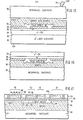
- a seed wafer 20, illustrated in FIG. 1, is prepared from a (100) silicon wafer 22. For sake of example, let the silicon wafer 22 have p doping.
- a silicon epitaxial layer 24 is grown on top of the silicon wafer 22.
- An insulating layer 26 is then formed on top of the epitaxial layer 24 by depositing a boron-rich quartz. This quartz can be a borosilicate glass which matches the thermal expansion properties of silicon.
- the seed wafer 20 is then placed on top of a silicon substrate wafer 28 with the insulating layer 26 contacting the substrate layer 28, as shown in FIG. 2.
- the two wafers 20 and 28 are then anodically bonded by the method taught in the previously cited patent 3,595,719.
- This bonding forms a true hermetic seal between the two wafers 20 and 28.
- the formation and nature of this bonding seal are described by Wallis et al in an article entitled “Field Assisted Glass Metal Sealing" appearing in the Journal of Applied Physics, Vol. 40, No. 10, 1969 at page 3946 and by Brooks et al in an article entitled “Low Temperature Electrostatic Silicon to Silicon Seals Using Sputtered Borosilicate Glass” appearing in the Journal of the Electrochemical Society, Vol. 119. No. 4, 1972 at page 545.
- the bonded wafers 20 and 28 are then dip etched to remove the region of the silicon wafer 22 and to produce the structure illustrated in FIG. 3.
- This structure has a surface epitaxial layer 24 separated from the silicon substrate 28 by the insulating layer 26.
- One of the purposes of this invention is to provide a method of defining elements below the insulating layer 26 and to use parts of that layer 26 as field barriers. It should be recognized that if elements had been defined in the silicon substrate 28 before the anodic bonding it would be difficult to align to those elements because of the featureless epitaxial surface of the structure of FIG. 3.
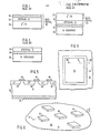
- a wafer In integrated circuit fabrication, a wafer usually contains many dice. Each die is a complete integrated circuit and the circuit pattern is replicated among a large number of dice.
- a die 30 is shown in FIG. 4 on a wafer 32. It is to be understood that the die is repeated in two dimensions in a rectangular close packed structure. However, surrounding each die 30 is a kerf region 34.
- a mechanical saw is applied to the kerf region 34 between the dice 30, thereby separating the dice but also destroying the kerf region 34.
- alignce marks are put in the kerf region 34 in order to allow proper registration between different levels of the semiconductor fabrication.
- the alignment marks can be put into peripheral regions of the wafer 32. Providing for the alignment marks is one of the first steps in one of the embodiments in this invention.
- Processing in a first embodiment of the invention begins with a cleaned standard silicon wafer 36, shown in FIG. 5, with n or p doping and an exposed (100) face.
- the wafer 36 has a back-side protect 38 such as an oxide or Si 3 N 4 .
- a diffusion masking oxide is grown on the front surface of the wafer 36 and this oxide is opened in a photoresist masking step to leave a series of small blocking oxide regions 40, 42 and 44.
- the pattern of the oxide regions 40-44 provides the alignment marks, illustrated in FIG. 6. The illustrated pattern is for five marks but other patterns can be used. All the alignment marks should appear in the anticipated kerf region 34 or alternatively in the wafer periphery.
- a p boron deposition and diffusion are made to provide a precision etch stop consisting of multiple stop regions 46, 48, 50 and 52, shown in FIG. 5.
- the p doping is 5 x 10 19 /cm 3 or above. It is to be understood that the stop region 46 extends over a substantial area of the die 30.
- the front side blocking oxide regions 40-44 are then removed and an n-type epitaxial layer 54 is grown on top of the silicon wafer 36 and its stop regions 46-52, as shown in FIG. 7.
- a standard n emitter layer 56 is applied on top of the epitaxial layer 54.
- the emitter layer 56 can be either blanket diffused or result from an ion implantation of the epitaxial layer 54. If desired, the emitter layer 56 could have been masked into individual regions for further device definition utilizing the alignment marks shown in FIG. 6.
- a thin gate dielectric layer 58 is then grown or deposited over the surface of the emitter layer 56, as shown in FIG. 8.
- the thickness of the dielectric layer 58 is somewhat arbitrary.
- a thin layer provides high capacitance but current technology sets a minimum thickness of 5nm to prevent defects. Its composition is also somewhat arbitrary but good adhesion to silicon is required.
- Dielectric layers 58 of Si0 2 are acceptable or a thin layer of SiO 2 for adhesion combined with a thicker si 3 N 4 layer may be used.
- the alignment marks of FIG. 6 are buried, they are apparent through the overlaying layers. Using these alignment marks, the gate dielectric layer 58 is patterned by standard photolithographic techniques to produce the structure shown in FIG. 8.
- FIG. 8 includes a larger portion of the area of the die 30 along the cross-sectional line VII-VII, in FIG. 4, rather than along the shorter cross-sectional line V-V, which concentrates on the kerf region 34.
- FIG. 8 illustrates that the openings 60 and 62 are linear with the stop regions 48-52 defining the alignment marks, in fact, the openings 60 and 62 may be of any number and located anywhere within the area of the die 30 independently of the location of the alignment marks within the kerf region 34.
- the dielectric layer 58 is a singie thickness. However this layer 58 can be patterned to different thickness if high capacitances are desired for only a portion of the integrated circuit while low capacitances are desired in other portions where the field shield is being used not as a capacitor but for wiring or for a shield against mobile ions.
- a layer of doped polysilicon or silicide or some other conductor is deposited on top of the gate dielectric layer 58 and is photo-lithographically defined, as shown in FIG. 9, to form a field shield 64.
- the field shield 64 extends over the major portion of the area of the die to provide a field shield for nearly the entire integrated circuit. In other embodiments, the field shield 64 is used for buried wiring so that its patterning is complex.
- an insulating SOI (silicon on insulator) layer 66 is deposited on top of the gate dielectric 58 and the field shield 64.
- the SOI insulating layer 66 should be a boron-rich glass which is deposited over the entire area either by sputtering or perhaps by chemical vapor deposition.
- An example of such a material is quartz.
- the sputtering procedure is described by Brooks et al in the previously cited article and the CVD process is described by Werner Kern in a technical article entitled "Chemical Vapor Deposition of Inorganic Class Films" appearing in Semiconductor International, March 1982 at pp. 89-103.
- the thick quartz layer 66 tends to planarize the surface to a limited extent.
- the quartz should match the thermal expansion coefficient of silicon. This condition is satisfied by a 17% boron content. Phosphorus rich glasses or a combination of phosphorus and boron can be used but a higher phosphorus content is required for the thermal matching. Sodium, such as is contained in PYREX, should not be used because of its degradation of dielectric-semiconductor interfaces.
- the thickness of the quartz should be in the range of 5-10 pm to minimize capacitance to the substrate.
- the back-side protect 38 is removed at this point.
- the resultant structure of FIG. 9 is the completed seed wafer that is used in SOI fabrication similarly to the seed wafer 20 of FIG. 1.
- the seed substrate of FIG. 9 is then anodically bonded to a mechanical substrate 68 as shown in FIG. 10.
- the mechanical substrate 68 may be a wafer of crystalline silicon.
- the bonding voltage for a quartz layer of 7 um thickness is in the range of 35-50 V.
- the field shield 64 is at the same potential as the seed substrate 36 during bonding, thereby preventing an electrostatic field build-up across the thin insulating gate dielectric 58.
- the polysilicon or other material in the field shield 64 provides a diffusion barrier against any mobile ions which might otherwise migrate from the boron-rich quartz 66 into the thin dielectric region 58 beneath the field shield 64. These mobile ions would cause problems with the subsequent operation of the fabricated devices in the area of the die.
- the field shield 64 can be used, not for its electrical characteristics, but as a diffusion shield against mobile ions migrating from the quartz 66.
- the high energy density pulse at the initial phase of the anodic bonding increases the temperature at the local bonding site by as such as 560°C which allows microscopic reflow of the quartz around non-planar features.
- the high local pressure causes a temporary decrease of the quartz viscosity around any protrusion at the bond interface. The reflow process has been described in the previously cited article by Wallis et al.
- the electrostatic field and microscopic fusing occurs at the interface 70 between the quartz 66 and the mechanical substrate 68, thereby eliminating the possible problem mentioned by Barth in an article entitled "Silicon Sensors Meet Integrated Circuits" appearing in IEEE Spectrum, September 1981, at page 33.
- This problem concerns possible damage to existing semiconductor structures caused by electrostatic discharges induced by the anodic bonding.
- the epitaxial layer 54 of the seed wafer is far removed from the bonding activity at the interface 70. It is the mechanical substrate 68 that suffers the electrical surface property degradation during bonding, not the silicon substrate 36 of the seed wafer or its epitaxial layer 54.
- the bonded wafer pair of FIG. 10 is then dip etched, perhaps using an anisotropic etch such as ethylene diamine pyrocatechol (EDP) to remove all the silicon in the seed wafer down to the p gate etch stop 46 in a process called etch-back.
- EDP ethylene diamine pyrocatechol
- the use of EDP is described by Kurt Petersen in a technical article entitled "Silicon as a Mechanical Material" appearing in the IEEE Proceedings, Vol. 70, No. 5, May 1982 at pp. 420-457. It should be noted that the backside of the mechanical substrate needs to be protected by an oxide during the etch-back. For a quicker etch, a majority of the etching is performed with a caustic with the final anisotropic etch done by EDP.
- the general principle of the EDP etch-back is that EDP readily etches silicon with doping concentrations below 10 19 /cm 3 but is ineffective at etching the p etch stop having a doping concentration above 5 x 10 19 /cm 3 .
- the resultant structure is shown in FIG. 11 in which the wafers have been turned upside-down from FIG. 10. However, in the vicinity of the alignment marks, the etch stop regions 46-52 are not continuous so that the etching in that region continues into the epitaxial layer 54 to form pyramids 70 and 72.
- the structure of one pyramid 70 is shown more accurately and in more detail in FIG. 12.
- the sides of the pyramid 70 slope at an angle of 54.7° with respect to the surface because of the anisotropic nature of the etch.
- the etching stops at the interface with the dielectric layer 58 with no additional undercutting if the wafer is left in the etch bath for more than the normal time.
- the pyramids 70 and 72 or the valleys between them provide alignment marks on an otherwise featureless surface of the p + etch stop layer 46.
- the pyramids 70 and 72 are necessarily aligned with whatever definition has been previously performed on the dielectric layer 58 or the field shield 64.
- the p etch stop regions 46-52 are etched away with an echant such as hydrofluoric-nitric-acetic acid (HNA) in the proportions 1:3:8 that leaves the structure illustrated in FIG. 13.
- HNA hydrofluoric-nitric-acetic acid
- the etchant is chosen such that it etches only silicon above a certain dopant concentration so that the p + gate etch stop 46 defines the precise limits of etching.
- HNA etchant is described by Muraoka et al in a chapter entitled “Controlled Preferential Etching Technology" appearing at page 327 in the book “Semiconductor Silicon 1973", Electrochemical Society Symposium Series (Princeton, N.J., 1973), edited by Huff et al.
- the HNA etch intended for the etch stop layer 46, would never reach the n + layer 56, thus preventing undercutting.
- This additional masking of the n layer 56 could also be used for buried device fabrication within the area of the die 30. Note that since the alignment marks appear in the kerf region 34, they would vanish upon dicing, thus not revealing how the alignment to the buried structure was accomplished.
- Transistors have been fabricated with the above approach but have been found to suffer unacceptable current leakage. It has been determined that when the etch stop regions 46-52 have doping levels above 3 x 10 19 / cm 3 , crystal slips form therein. These slip defects propagate through the epitaxial layer 54 producing the observed degradation. Accordingly, a second and preferred embodiment of the invention has been developed using a different etch-stop technique and using laser scribing for back-side alignment.
- Fabrication in the second embodiment begins with a heavily doped g + seed substrate 80, shown in FIG. 15, on which is grown the n epitaxial layer 54. There is no explicit etch-stop in this embodiment but the interface 82 between the lightly doped n - epitaxial layer 54 and the heavily doped p + seed substrate 80 provides the etch stopping characteristics to be described later. Then the n emitter layer 56 and the thin dielectric layer 58 are grown just as in the first embodiment.
- a laser is used to provide alignment marks on the dielectric layer 58.
- This procedure is described in a patent application Serial Number , filed by one of the inventors, P. Cade on and entitled, "Laser Process for Forming Identically Positioned Alignment Marks on the Opposite Sides of a Semiconductor Wafer".
- the advantage of the laser scribing techniques is that the laser scribed marks propagate from the surface of the dielectric layer 58 through at least the epitaxial layer 54, thus providing back-to-front registry.
- the field shield 64 and the boron-rich quartz 66 are likewise formed by similar procedures using the laser-scribed alignment marks for any required definition including possible definition of the emitter layer 56.
- the mechanical substrate 68 of silicon is then anodically bonded to the quartz 66 by applyiag voltage to a voltage probe 84 with the seed substrate 80 grounded.
- the etch-back of the seed substrate 80 is performed with hydrofluoric-nitric-acetic aeid (HNA) in the proportions of 1:3:8.
- HNA hydrofluoric-nitric-acetic aeid
- the etchant HNA is an isotropic etch and attacks heavily doped p + or n silicon. However, it does not appreciably attack silicon doped below the level of 10 18 /cm 3 .
- the etch stopping characteristics are improved by the p /n junction at the interface 82.
- the HNA etchant also attacks silicon oxide to some degree. Accordingly, the etching is divided into two steps.
- the first major part of the etching is performed with a caustic.
- the final gart of the etch is performed with HNA to provide the precise etch-stopping characteristics.
- Whatever etching of the oxide protect of the mechanical substrate 68 occurs is insufficient to break through the oxide protect.
- the resultant strsetare after the etch-back is illustrated in FIG. 16.
- Not shown in this Figure are the laser scribed registration marks which are visible at the top side of the epitaxial layer 54 on an otherwise featureless surface. These etch marks are aligned with the field shield 64 and whatever definition has been performed in the emitter layer 56. It is seen that the structure of FIG. 16 closely resembles that of FIG. 13, except for the alignment marks.
- FIG. 17 An example of an integrated circuit built using the substrate of this invention is illustrated in FIG. 17.
- Two storage cells 90 and 92 chosen for illustrative purposes, each have a vertical transistor consisting of a diffused n region 94, a diffused p region 96 and an epitaxial n region 98.
- the epitaxial n region 98 is part of the epitaxial layer 54 of the substrate of FIGS. 13 and 16.
- Underlying the epitaxial n region 98 is an n layer 100 which is formed from the emitter step layer 56 of FIGS. 13 and 16.
- a storage node with high capacitance results from the n layer 100, a thin dielectric layer 102 and a buried field shield 104.
- the dielectric layer 102 and the field shield 104 are equivalent to the corresponding elements 58 and 64 in FIGS. 13 and 16.
- the field shield 104 is connected to the surface by field shield reach-throughs or contacts 106 and 108.
- Support transistors 110 and 112 are formed in an area of the die away from the field shield 104.
- the transistor 110 consists of a diffused n region 114, a diffused p region 116 and an n epitaxial layer 118.
- a planar contact is made to the n epitaxial layer 118 with an n layer 120 connected to the surface with a diffused n reach-through 122.
- the support transistors 110 and 112, the field shield contacts 106 and 108 and the storage cells are all isolated by dielectric trenches 124 extending from the surface to the dielectric layer 58. The required surface interconnections are not shown.
Landscapes
- Engineering & Computer Science (AREA)
- Computer Hardware Design (AREA)
- Microelectronics & Electronic Packaging (AREA)
- Power Engineering (AREA)
- Physics & Mathematics (AREA)
- Condensed Matter Physics & Semiconductors (AREA)
- General Physics & Mathematics (AREA)
- Manufacturing & Machinery (AREA)
- Element Separation (AREA)
- Semiconductor Integrated Circuits (AREA)
Abstract
Description
- The invention pertains generally to integrated circuits. In particular, it pertains to the fabrication of a buried field shield beneath semiconductor devices on an integrated circuit chip.
- A technology for integrated circuits must be judged on at least two criteria besides the obvious need for practicality of fabrication. The devices should be densely packed on the integrated circuit to allow a large number of individual devices on a small area chip. Furthermore, the devices must be fast so that the integrated circuit has a high throughput. The speed of most technologies is limited by stray capacitance, both between devices and to the substrate. Many recent designs, such as those disclosed by Rao in U.S. Patent No. 4,388,121 and by Koomen et al in U.S. Patent No. 4,317,690, have attempted to reduce the area by using multi-layer structures so that two separate elements are occupying the same surface area and no area is occupied by their interconnects. This approach, however, introduces capacitance between the layers. Futhermore, these devices are usually built on a semiconductor substrate so that there is an unavoidable capacitance to the substrate. It should be noted that, in some situations, a high capacitance is desired, such as in dynamic memory cells. If the capacitance per area of the memory cell can be increased, the total area of the memory cell can be decreased, resulting in a high chip density. A further advantage of high capacitance for small area memory cells is the immunity to alpha particles. Thus, it is desirable to simultaneously have low capacitance and high capacitance areas on the same integrated circuit.
- One technology that eliminates substrate capacitance is silicon on sapphire (SOS). In SOS, a layer of silicon is grown on top of an insulating sapphire substrate. As a result, substrate capacitance is negligible. However, SOS tends to require fairly large surface areas and multi-layer SOS devices are not common.
- A recent variant of SOS is silicon on insulator (SOI), in which a silicon layer is formed on top of a layer of silicon dioxide. A description of SOI technology is contained in a technical article by A. Jastrzebski, appearing in the RCA Review, Vol. 44, June 1983 at pp.250-269 and entitled "Comparison of Different SOI Technologies: Assets and Liabilities".
- Accordingly, it is an object of this invention to provide for the fabrication of dense integrated circuits.
- It is a further object of this invention to provide for the fabrication of multi-layered devices on an integrated circuit chip.
- It is yet a further object of this invention to provide both high and low capacitance areas on the same integrated circuit chip.
- The invention provides a buried conductive field shield separated by a thin dielectric layer from the epitaxial region in an SOI integrated circuit. The epitaxial layer is grown upon a seed wafer and the thin dielectric layer and the conductive shield are deposited upon the epitaxial layer. A thick layer of quartz is then deposited and the quartz is mechanically bonded to a mechanical substrate. The original seed wafer is then removed to expose the epitaxial layer for definition of the integrated circuit. The field shield lies beneath the epitaxial layer and can be used for high capacitance elements, for buried wiring and for shielding the epitaxial layer against migration of mobile ions from the quartz.
-
- FIGS. 1-3 illustrate a conventional method of producing a silicon on insulator structure by anodic bonding.
- FIG. 4 illustrates a die and its kerf region.
- FIG. 5 is a crose-seetional illustration of a first step of one embodiment of the present invention.
- FIG. 6 illustrates alignment marks on a wafer.
- FIGS. 7-11 and 13 are cross-sectional illustrations of further steps in the first embodiment, with FIG. 13 being the final structure.
- FIG. 12 is an enlarged cross-sectional view of an alignment mark.
- FIG. 14 is an enlarged cross-section of the alignment marks in a variation of the first embodiment.
- FIGS. 15 and 16 are cross-sectional illustrations of steps in a second and preferred embodiment of the invention.
- FIG. 17 is a cross-sectional illustration of a circuit that can be produced by means of the invention.
- This invention provides a simple method for fabricating a buried field shield in an integrated circuit. The buried field shield is a thin conductive layer that lies below a semiconductor region in the integrated circuit chip and is separated from the semiconductor region by a thin dielectric layer. Such a buried field shield can be used, for example, for memory storage cells and produces additional dielectric film capacitance below the active devices without increasing the required surface area.
- The method of this invention relies upon a recently developed technique for fabricating a buried insulating layer in a semiconductor material. This method is based on disclosures by Pomerantz in U.S. Patent No. 3,595,719, and Antypas in U.S. Patent No. 3,959,045, and Kimura et al in a technical article entitled "Epitaxial Film Transfer Technique for Producing Single Crystal Si Film on an Insulating Substrate" appearing in Applied Physics Letters, Vol. 43, No. 3, August 1, 1983 at pp. 263-265. Additional references for the bonding of two wafers are U.S. Patent Nos. 3,332,137, 4,384,899 and 4,389,276, German Patentschrift 593,559 and Japanese patent document 56-106430.
- A
seed wafer 20, illustrated in FIG. 1, is prepared from a (100)silicon wafer 22. For sake of example, let thesilicon wafer 22 have p doping. A siliconepitaxial layer 24 is grown on top of thesilicon wafer 22. Aninsulating layer 26 is then formed on top of theepitaxial layer 24 by depositing a boron-rich quartz. This quartz can be a borosilicate glass which matches the thermal expansion properties of silicon. - The
seed wafer 20 is then placed on top of asilicon substrate wafer 28 with theinsulating layer 26 contacting thesubstrate layer 28, as shown in FIG. 2. The twowafers wafers - The
bonded wafers silicon wafer 22 and to produce the structure illustrated in FIG. 3. This structure has a surfaceepitaxial layer 24 separated from thesilicon substrate 28 by theinsulating layer 26. One of the purposes of this invention is to provide a method of defining elements below theinsulating layer 26 and to use parts of thatlayer 26 as field barriers. It should be recognized that if elements had been defined in thesilicon substrate 28 before the anodic bonding it would be difficult to align to those elements because of the featureless epitaxial surface of the structure of FIG. 3. - In integrated circuit fabrication, a wafer usually contains many dice. Each die is a complete integrated circuit and the circuit pattern is replicated among a large number of dice. A die 30 is shown in FIG. 4 on a
wafer 32. It is to be understood that the die is repeated in two dimensions in a rectangular close packed structure. However, surrounding each die 30 is akerf region 34. When the wafer fabrication is completed, a mechanical saw is applied to thekerf region 34 between thedice 30, thereby separating the dice but also destroying thekerf region 34. In one embodiment of the present invention, aligmment marks are put in thekerf region 34 in order to allow proper registration between different levels of the semiconductor fabrication. Alternatively, the alignment marks can be put into peripheral regions of thewafer 32. Providing for the alignment marks is one of the first steps in one of the embodiments in this invention. - Processing in a first embodiment of the invention begins with a cleaned
standard silicon wafer 36, shown in FIG. 5, with n or p doping and an exposed (100) face. Thewafer 36 has a back-side protect 38 such as an oxide or Si3N4. A diffusion masking oxide is grown on the front surface of thewafer 36 and this oxide is opened in a photoresist masking step to leave a series of smallblocking oxide regions kerf region 34 or alternatively in the wafer periphery. Multiple sets of alignment marks are required for the integrated circuit but it is not necessary that they appear next to each die 30. Then a p boron deposition and diffusion are made to provide a precision etch stop consisting ofmultiple stop regions stop region 46 extends over a substantial area of thedie 30. - The front side blocking oxide regions 40-44 are then removed and an n-
type epitaxial layer 54 is grown on top of thesilicon wafer 36 and its stop regions 46-52, as shown in FIG. 7. A standardn emitter layer 56 is applied on top of theepitaxial layer 54. Theemitter layer 56 can be either blanket diffused or result from an ion implantation of theepitaxial layer 54. If desired, theemitter layer 56 could have been masked into individual regions for further device definition utilizing the alignment marks shown in FIG. 6. - A thin
gate dielectric layer 58 is then grown or deposited over the surface of theemitter layer 56, as shown in FIG. 8. The thickness of thedielectric layer 58 is somewhat arbitrary. A thin layer provides high capacitance but current technology sets a minimum thickness of 5nm to prevent defects. Its composition is also somewhat arbitrary but good adhesion to silicon is required.Dielectric layers 58 of Si02 are acceptable or a thin layer of SiO2 for adhesion combined with a thicker si3N4 layer may be used. Although the alignment marks of FIG. 6 are buried, they are apparent through the overlaying layers. Using these alignment marks, thegate dielectric layer 58 is patterned by standard photolithographic techniques to produce the structure shown in FIG. 8. The patterns on thedielectric layer 58 provideopenings die 30 along the cross-sectional line VII-VII, in FIG. 4, rather than along the shorter cross-sectional line V-V, which concentrates on thekerf region 34. Although FIG. 8 illustrates that theopenings openings kerf region 34. - In the embodiment illustrated in FIG. 8, the
dielectric layer 58 is a singie thickness. However thislayer 58 can be patterned to different thickness if high capacitances are desired for only a portion of the integrated circuit while low capacitances are desired in other portions where the field shield is being used not as a capacitor but for wiring or for a shield against mobile ions. - Then a layer of doped polysilicon or silicide or some other conductor is deposited on top of the
gate dielectric layer 58 and is photo-lithographically defined, as shown in FIG. 9, to form afield shield 64. In one embodiment, thefield shield 64 extends over the major portion of the area of the die to provide a field shield for nearly the entire integrated circuit. In other embodiments, thefield shield 64 is used for buried wiring so that its patterning is complex. - In the final step of the preparation of the seed wafer, an insulating SOI (silicon on insulator)
layer 66 is deposited on top of thegate dielectric 58 and thefield shield 64. TheSOI insulating layer 66 should be a boron-rich glass which is deposited over the entire area either by sputtering or perhaps by chemical vapor deposition. An example of such a material is quartz. The sputtering procedure is described by Brooks et al in the previously cited article and the CVD process is described by Werner Kern in a technical article entitled "Chemical Vapor Deposition of Inorganic Class Films" appearing in Semiconductor International, March 1982 at pp. 89-103. Note that thethick quartz layer 66 tends to planarize the surface to a limited extent. The quartz should match the thermal expansion coefficient of silicon. This condition is satisfied by a 17% boron content. Phosphorus rich glasses or a combination of phosphorus and boron can be used but a higher phosphorus content is required for the thermal matching. Sodium, such as is contained in PYREX, should not be used because of its degradation of dielectric-semiconductor interfaces. The thickness of the quartz should be in the range of 5-10 pm to minimize capacitance to the substrate. The back-side protect 38 is removed at this point. The resultant structure of FIG. 9 is the completed seed wafer that is used in SOI fabrication similarly to theseed wafer 20 of FIG. 1. - The seed substrate of FIG. 9 is then anodically bonded to a
mechanical substrate 68 as shown in FIG. 10. Themechanical substrate 68 may be a wafer of crystalline silicon. The bonding voltage for a quartz layer of 7 um thickness is in the range of 35-50 V. There are a number of important points to be explained for this bonding step. Thefield shield 64 is at the same potential as theseed substrate 36 during bonding, thereby preventing an electrostatic field build-up across the thin insulatinggate dielectric 58. The polysilicon or other material in thefield shield 64 provides a diffusion barrier against any mobile ions which might otherwise migrate from the boron-rich quartz 66 into the thindielectric region 58 beneath thefield shield 64. These mobile ions would cause problems with the subsequent operation of the fabricated devices in the area of the die. Thefield shield 64 can be used, not for its electrical characteristics, but as a diffusion shield against mobile ions migrating from thequartz 66. - The regions where the polysilicon field shield does not protect the thin insulating
gate layer 58 are nonetheless protected from inversion by then stop layer 56 on top of theepitaxial layer 54. - The non-planarity of the quartz surface, illustrated in FIG. 9, is not a major concern for the anodic bonding. In fact, anodic bonding has been demonstrated on top of aluminum wiring patterns. Such successful bonding over defined features is described in a technical article by Roylance et al entitled "A Batch-Fabricated Silicon Accelerometer" and appearing in IEEE Transactions on Electron Devices, Vol. ED-26, No. 12, 1979 at page 1911 and in a technical article by Sander et al, entitled "Monolithic Capacitive Pressure Sensor With Pulse-Period Output" and appearing in IEEE Transactions on Electron Devices, Vol. ED-27, No. 5, 1980 at page 927. It has been suggested that the high energy density pulse at the initial phase of the anodic bonding increases the temperature at the local bonding site by as such as 560°C which allows microscopic reflow of the quartz around non-planar features. However, we believe that the high local pressure causes a temporary decrease of the quartz viscosity around any protrusion at the bond interface. The reflow process has been described in the previously cited article by Wallis et al.
- The electrostatic field and microscopic fusing occurs at the
interface 70 between thequartz 66 and themechanical substrate 68, thereby eliminating the possible problem mentioned by Barth in an article entitled "Silicon Sensors Meet Integrated Circuits" appearing in IEEE Spectrum, September 1981, at page 33. This problem concerns possible damage to existing semiconductor structures caused by electrostatic discharges induced by the anodic bonding. Theepitaxial layer 54 of the seed wafer is far removed from the bonding activity at theinterface 70. It is themechanical substrate 68 that suffers the electrical surface property degradation during bonding, not thesilicon substrate 36 of the seed wafer or itsepitaxial layer 54. - The bonded wafer pair of FIG. 10 is then dip etched, perhaps using an anisotropic etch such as ethylene diamine pyrocatechol (EDP) to remove all the silicon in the seed wafer down to the p
gate etch stop 46 in a process called etch-back. The use of EDP is described by Kurt Petersen in a technical article entitled "Silicon as a Mechanical Material" appearing in the IEEE Proceedings, Vol. 70, No. 5, May 1982 at pp. 420-457. It should be noted that the backside of the mechanical substrate needs to be protected by an oxide during the etch-back. For a quicker etch, a majority of the etching is performed with a caustic with the final anisotropic etch done by EDP. The general principle of the EDP etch-back is that EDP readily etches silicon with doping concentrations below 1019/cm3 but is ineffective at etching the p etch stop having a doping concentration above 5 x 10¹⁹/cm3. The resultant structure is shown in FIG. 11 in which the wafers have been turned upside-down from FIG. 10. However, in the vicinity of the alignment marks, the etch stop regions 46-52 are not continuous so that the etching in that region continues into theepitaxial layer 54 to formpyramids pyramid 70 is shown more accurately and in more detail in FIG. 12. The sides of thepyramid 70 slope at an angle of 54.7° with respect to the surface because of the anisotropic nature of the etch. The etching, however, stops at the interface with thedielectric layer 58 with no additional undercutting if the wafer is left in the etch bath for more than the normal time. Thepyramids etch stop layer 46. Thepyramids dielectric layer 58 or thefield shield 64. - The p etch stop regions 46-52 are etched away with an echant such as hydrofluoric-nitric-acetic acid (HNA) in the proportions 1:3:8 that leaves the structure illustrated in FIG. 13. The etchant is chosen such that it etches only silicon above a certain dopant concentration so that the p+
gate etch stop 46 defines the precise limits of etching. This HNA etchant is described by Muraoka et al in a chapter entitled "Controlled Preferential Etching Technology" appearing at page 327 in the book "Semiconductor Silicon 1973", Electrochemical Society Symposium Series (Princeton, N.J., 1973), edited by Huff et al. It is also described by Maggiore et al in an article entitled "Thin Epitaxial dE/dx Detectors" appearing in IEEE Transactions on Nuclear Science, Vol. NS-24, No. 1, 1977 at page 104. If then deposition 56 onto theepitaxial layer 54 was applied as a blanket across the entire wafer, as shown in FIG. 7, the final etching step produces undercutting of thepyramids epitaxial layer 54, as shown in FIG. 13. If, on the other hand, the deposition of then layer 56 were masked around the alignment marks, as illustrated in FIG. 14, the alignment pit could be left free of then layer 56. Then the HNA etch, intended for theetch stop layer 46, would never reach the n +layer 56, thus preventing undercutting. This additional masking of then layer 56 could also be used for buried device fabrication within the area of thedie 30. Note that since the alignment marks appear in thekerf region 34, they would vanish upon dicing, thus not revealing how the alignment to the buried structure was accomplished. - Transistors have been fabricated with the above approach but have been found to suffer unacceptable current leakage. It has been determined that when the etch stop regions 46-52 have doping levels above 3 x 10¹⁹/cm 3, crystal slips form therein. These slip defects propagate through the
epitaxial layer 54 producing the observed degradation. Accordingly, a second and preferred embodiment of the invention has been developed using a different etch-stop technique and using laser scribing for back-side alignment. - Fabrication in the second embodiment begins with a heavily doped g+ seed substrate 80, shown in FIG. 15, on which is grown the
n epitaxial layer 54. There is no explicit etch-stop in this embodiment but theinterface 82 between the lightly doped n- epitaxial layer 54 and the heavily doped p+ seed substrate 80 provides the etch stopping characteristics to be described later. Then then emitter layer 56 and thethin dielectric layer 58 are grown just as in the first embodiment. - At this point, a laser is used to provide alignment marks on the
dielectric layer 58. This procedure is described in a patent application Serial Number , filed by one of the inventors, P. Cade on and entitled, "Laser Process for Forming Identically Positioned Alignment Marks on the Opposite Sides of a Semiconductor Wafer". The advantage of the laser scribing techniques is that the laser scribed marks propagate from the surface of thedielectric layer 58 through at least theepitaxial layer 54, thus providing back-to-front registry. - The
field shield 64 and the boron-rich quartz 66 are likewise formed by similar procedures using the laser-scribed alignment marks for any required definition including possible definition of theemitter layer 56. Themechanical substrate 68 of silicon is then anodically bonded to thequartz 66 by applyiag voltage to avoltage probe 84 with theseed substrate 80 grounded. - The etch-back of the
seed substrate 80 is performed with hydrofluoric-nitric-acetic aeid (HNA) in the proportions of 1:3:8. The etchant HNA is an isotropic etch and attacks heavily doped p+ or n silicon. However, it does not appreciably attack silicon doped below the level of 1018/cm3. The etch stopping characteristics are improved by the p /n junction at theinterface 82. In order to prevent the etching of the siliconmechanical substrate 68 the backside of the mechanical substrate is protected with an oxide during the etch-back. However, the HNA etchant also attacks silicon oxide to some degree. Accordingly, the etching is divided into two steps. The first major part of the etching is performed with a caustic. The final gart of the etch is performed with HNA to provide the precise etch-stopping characteristics. Whatever etching of the oxide protect of themechanical substrate 68 occurs is insufficient to break through the oxide protect. The resultant strsetare after the etch-back is illustrated in FIG. 16. Not shown in this Figure are the laser scribed registration marks which are visible at the top side of theepitaxial layer 54 on an otherwise featureless surface. These etch marks are aligned with thefield shield 64 and whatever definition has been performed in theemitter layer 56. It is seen that the structure of FIG. 16 closely resembles that of FIG. 13, except for the alignment marks. - At this point, normal processing of the substrate of either FIG. 13 or 16 proceeds upon the area of the die 30 which has a smooth surface of the
epitaxial layer 54 and has a buriedfield shield 64 underlying that die area. Thepyramids dielectric layer 58 and the field shield, not themselves visible. It is anticipated that then region 56 is delineated on top of thedielectric layer 58 so that devices, such as capacitors, can be fabricated using both the insulatinglayer 58 and thefield shield 64 as constituent elements. - An example of an integrated circuit built using the substrate of this invention is illustrated in FIG. 17. Two
storage cells epitaxial layer 54 of the substrate of FIGS. 13 and 16. Underlying the epitaxial n region 98 is an n layer 100 which is formed from theemitter step layer 56 of FIGS. 13 and 16. A storage node with high capacitance results from the n layer 100, a thin dielectric layer 102 and a buried field shield 104. The dielectric layer 102 and the field shield 104 are equivalent to thecorresponding elements contacts Support transistors transistor 110 consists of a diffused n region 114, a diffused p region 116 and an n epitaxial layer 118. A planar contact is made to the n epitaxial layer 118 with an n layer 120 connected to the surface with a diffused n reach-through 122. Thesupport transistors field shield contacts dielectric trenches 124 extending from the surface to thedielectric layer 58. The required surface interconnections are not shown.
Claims (9)
Applications Claiming Priority (2)
| Application Number | Priority Date | Filing Date | Title |
|---|---|---|---|
| US06/620,982 US4599792A (en) | 1984-06-15 | 1984-06-15 | Buried field shield for an integrated circuit |
| US620982 | 1996-03-22 |
Publications (3)
| Publication Number | Publication Date |
|---|---|
| EP0164646A2 true EP0164646A2 (en) | 1985-12-18 |
| EP0164646A3 EP0164646A3 (en) | 1987-08-05 |
| EP0164646B1 EP0164646B1 (en) | 1989-08-09 |
Family
ID=24488231
Family Applications (1)
| Application Number | Title | Priority Date | Filing Date |
|---|---|---|---|
| EP85106580A Expired EP0164646B1 (en) | 1984-06-15 | 1985-05-29 | Buried field shield for an integrated circuit |
Country Status (4)
| Country | Link |
|---|---|
| US (1) | US4599792A (en) |
| EP (1) | EP0164646B1 (en) |
| JP (1) | JPS614269A (en) |
| DE (1) | DE3572259D1 (en) |
Cited By (7)
| Publication number | Priority date | Publication date | Assignee | Title |
|---|---|---|---|---|
| EP0256397A1 (en) * | 1986-07-31 | 1988-02-24 | Hitachi, Ltd. | Semiconductor device having a burried layer |
| EP0486318A1 (en) * | 1990-11-15 | 1992-05-20 | Seiko Instruments Inc. | Semiconductor device for use in a light valve device, and process for manufacturing the same |
| US5434433A (en) * | 1992-08-19 | 1995-07-18 | Seiko Instruments Inc. | Semiconductor device for a light wave |
| US5574292A (en) * | 1992-05-13 | 1996-11-12 | Seiko Instruments Inc. | Semiconductor device with monosilicon layer |
| US5618739A (en) * | 1990-11-15 | 1997-04-08 | Seiko Instruments Inc. | Method of making light valve device using semiconductive composite substrate |
| US5633176A (en) * | 1992-08-19 | 1997-05-27 | Seiko Instruments Inc. | Method of producing a semiconductor device for a light valve |
| US6191476B1 (en) | 1992-10-21 | 2001-02-20 | Seiko Instruments Inc. | Semiconductor device |
Families Citing this family (21)
| Publication number | Priority date | Publication date | Assignee | Title |
|---|---|---|---|---|
| US4717681A (en) * | 1986-05-19 | 1988-01-05 | Texas Instruments Incorporated | Method of making a heterojunction bipolar transistor with SIPOS |
| US4774196A (en) * | 1987-08-25 | 1988-09-27 | Siliconix Incorporated | Method of bonding semiconductor wafers |
| JPH02168666A (en) * | 1988-09-29 | 1990-06-28 | Mitsubishi Electric Corp | Complementary semiconductor device and manufacture thereof |
| US5223735A (en) * | 1988-09-30 | 1993-06-29 | Mitsubishi Denki Kabushiki Kaisha | Semiconductor integrated circuit device in which circuit functions can be remedied or changed and the method for producing the same |
| US5013681A (en) * | 1989-09-29 | 1991-05-07 | The United States Of America As Represented By The Secretary Of The Navy | Method of producing a thin silicon-on-insulator layer |
| US5306942A (en) * | 1989-10-11 | 1994-04-26 | Nippondenso Co., Ltd. | Semiconductor device having a shield which is maintained at a reference potential |
| JPH03107994U (en) * | 1990-02-22 | 1991-11-06 | ||
| US5234860A (en) * | 1992-03-19 | 1993-08-10 | Eastman Kodak Company | Thinning of imaging device processed wafers |
| US5369304A (en) * | 1992-08-14 | 1994-11-29 | Motorola, Inc. | Conductive diffusion barrier of titanium nitride in ohmic contact with a plurality of doped layers therefor |
| US5395481A (en) * | 1993-10-18 | 1995-03-07 | Regents Of The University Of California | Method for forming silicon on a glass substrate |
| US5488012A (en) * | 1993-10-18 | 1996-01-30 | The Regents Of The University Of California | Silicon on insulator with active buried regions |
| US5498898A (en) * | 1993-12-28 | 1996-03-12 | Nippon Steel Corporation | Semiconductor device using element isolation by field shield |
| US5656510A (en) * | 1994-11-22 | 1997-08-12 | Lucent Technologies Inc. | Method for manufacturing gate oxide capacitors including wafer backside dielectric and implantation electron flood gun current control |
| US5650654A (en) * | 1994-12-30 | 1997-07-22 | International Business Machines Corporation | MOSFET device having controlled parasitic isolation threshold voltage |
| JPH08222710A (en) * | 1995-02-17 | 1996-08-30 | Mitsubishi Electric Corp | Semiconductor device |
| US5869386A (en) * | 1995-09-28 | 1999-02-09 | Nec Corporation | Method of fabricating a composite silicon-on-insulator substrate |
| US5888412A (en) * | 1996-03-04 | 1999-03-30 | Motorola, Inc. | Method for making a sculptured diaphragm |
| US6737337B1 (en) * | 2001-04-27 | 2004-05-18 | Advanced Micro Devices, Inc. | Method of preventing dopant depletion in surface semiconductor layer of semiconductor-on-insulator (SOI) device |
| US6593221B1 (en) | 2002-08-13 | 2003-07-15 | Micron Technology, Inc. | Selective passivation of exposed silicon |
| DE10350038A1 (en) * | 2003-10-27 | 2005-05-25 | Robert Bosch Gmbh | Method for anodic bonding of wafers and device |
| KR101548173B1 (en) * | 2008-09-18 | 2015-08-31 | 삼성전자주식회사 | Wafer temporary bonding method using Si direct bondingSDB and semiconductor device and fabricating method thereof using the same bonding method |
Citations (5)
| Publication number | Priority date | Publication date | Assignee | Title |
|---|---|---|---|---|
| US3602982A (en) * | 1967-05-13 | 1971-09-07 | Philips Corp | Method of manufacturing a semiconductor device and device manufactured by said method |
| DE2526507A1 (en) * | 1974-06-24 | 1976-01-15 | Westinghouse Electric Corp | METHOD FOR PRODUCING A SEMICONDUCTOR LAYER |
| US3944447A (en) * | 1973-03-12 | 1976-03-16 | Ibm Corporation | Method for fabrication of integrated circuit structure with full dielectric isolation utilizing selective oxidation |
| DD134283A1 (en) * | 1977-11-24 | 1979-02-14 | Palmir M Gafarov | INTEGRATED SEMICONDUCTOR CIRCUIT AND METHOD FOR THE PRODUCTION THEREOF |
| US4216491A (en) * | 1975-10-15 | 1980-08-05 | Tokyo Shibaura Electric Co., Ltd. | Semiconductor integrated circuit isolated through dielectric material |
Family Cites Families (8)
| Publication number | Priority date | Publication date | Assignee | Title |
|---|---|---|---|---|
| US3846198A (en) * | 1972-10-02 | 1974-11-05 | Rca Corp | Method of making semiconductor devices having thin active regions of the semiconductor material |
| US3959045A (en) * | 1974-11-18 | 1976-05-25 | Varian Associates | Process for making III-V devices |
| JPS5269587A (en) * | 1975-12-08 | 1977-06-09 | Hitachi Ltd | Device and manufacture for high voltage resisting semiconductor |
| US4404737A (en) * | 1979-11-29 | 1983-09-20 | Tokyo Shibaura Denki Kabushiki Kaisha | Method for manufacturing a semiconductor integrated circuit utilizing polycrystalline silicon deposition, oxidation and etching |
| JPS56125868A (en) * | 1980-03-07 | 1981-10-02 | Chiyou Lsi Gijutsu Kenkyu Kumiai | Thin-film semiconductor device |
| US4290831A (en) * | 1980-04-18 | 1981-09-22 | Harris Corporation | Method of fabricating surface contacts for buried layer into dielectric isolated islands |
| US4408386A (en) * | 1980-12-12 | 1983-10-11 | Oki Electric Industry Co., Ltd. | Method of manufacturing semiconductor integrated circuit devices |
| JPS5948950A (en) * | 1982-09-13 | 1984-03-21 | Agency Of Ind Science & Technol | Manufacture of three-dimensional integrated circuit structure |
-
1984
- 1984-06-15 US US06/620,982 patent/US4599792A/en not_active Expired - Lifetime
-
1985
- 1985-01-31 JP JP60015637A patent/JPS614269A/en active Granted
- 1985-05-29 EP EP85106580A patent/EP0164646B1/en not_active Expired
- 1985-05-29 DE DE8585106580T patent/DE3572259D1/en not_active Expired
Patent Citations (5)
| Publication number | Priority date | Publication date | Assignee | Title |
|---|---|---|---|---|
| US3602982A (en) * | 1967-05-13 | 1971-09-07 | Philips Corp | Method of manufacturing a semiconductor device and device manufactured by said method |
| US3944447A (en) * | 1973-03-12 | 1976-03-16 | Ibm Corporation | Method for fabrication of integrated circuit structure with full dielectric isolation utilizing selective oxidation |
| DE2526507A1 (en) * | 1974-06-24 | 1976-01-15 | Westinghouse Electric Corp | METHOD FOR PRODUCING A SEMICONDUCTOR LAYER |
| US4216491A (en) * | 1975-10-15 | 1980-08-05 | Tokyo Shibaura Electric Co., Ltd. | Semiconductor integrated circuit isolated through dielectric material |
| DD134283A1 (en) * | 1977-11-24 | 1979-02-14 | Palmir M Gafarov | INTEGRATED SEMICONDUCTOR CIRCUIT AND METHOD FOR THE PRODUCTION THEREOF |
Cited By (15)
| Publication number | Priority date | Publication date | Assignee | Title |
|---|---|---|---|---|
| EP0256397A1 (en) * | 1986-07-31 | 1988-02-24 | Hitachi, Ltd. | Semiconductor device having a burried layer |
| EP0915503A2 (en) * | 1990-11-15 | 1999-05-12 | Seiko Instruments Inc. | Semiconductor device for use in a light valve device, and process for manufacturing the same |
| EP0486318A1 (en) * | 1990-11-15 | 1992-05-20 | Seiko Instruments Inc. | Semiconductor device for use in a light valve device, and process for manufacturing the same |
| US5347154A (en) * | 1990-11-15 | 1994-09-13 | Seiko Instruments Inc. | Light valve device using semiconductive composite substrate |
| EP1026733A1 (en) * | 1990-11-15 | 2000-08-09 | Seiko Instruments Inc. | Semiconductor device for use in a light valve device, and process for manufacturing the same |
| US5486708A (en) * | 1990-11-15 | 1996-01-23 | Seiko Instruments Inc. | Light valve device using semiconductive composite substrate |
| US5572045A (en) * | 1990-11-15 | 1996-11-05 | Seiko Instruments Inc. | Light valve device using semiconductive composite substrate |
| US5618739A (en) * | 1990-11-15 | 1997-04-08 | Seiko Instruments Inc. | Method of making light valve device using semiconductive composite substrate |
| EP0915503A3 (en) * | 1990-11-15 | 1999-05-19 | Seiko Instruments Inc. | Semiconductor device for use in a light valve device, and process for manufacturing the same |
| US5728591A (en) * | 1990-11-15 | 1998-03-17 | Seiko Instruments Inc. | Process for manufacturing light valve device using semiconductive composite substrate |
| US5574292A (en) * | 1992-05-13 | 1996-11-12 | Seiko Instruments Inc. | Semiconductor device with monosilicon layer |
| US5633176A (en) * | 1992-08-19 | 1997-05-27 | Seiko Instruments Inc. | Method of producing a semiconductor device for a light valve |
| US5434433A (en) * | 1992-08-19 | 1995-07-18 | Seiko Instruments Inc. | Semiconductor device for a light wave |
| US6187605B1 (en) | 1992-08-19 | 2001-02-13 | Seiko Instruments Inc. | Method of forming a semiconductor device for a light valve |
| US6191476B1 (en) | 1992-10-21 | 2001-02-20 | Seiko Instruments Inc. | Semiconductor device |
Also Published As
| Publication number | Publication date |
|---|---|
| DE3572259D1 (en) | 1989-09-14 |
| JPH0350420B2 (en) | 1991-08-01 |
| JPS614269A (en) | 1986-01-10 |
| EP0164646B1 (en) | 1989-08-09 |
| US4599792A (en) | 1986-07-15 |
| EP0164646A3 (en) | 1987-08-05 |
Similar Documents
| Publication | Publication Date | Title |
|---|---|---|
| US4599792A (en) | Buried field shield for an integrated circuit | |
| KR0163402B1 (en) | Merged bipolar/cmos technology using electrically active trench | |
| EP0166218B1 (en) | Silicon-on-insulator transistors | |
| US5767561A (en) | Integrated circuit device with isolated circuit elements | |
| US4566175A (en) | Method of making insulated gate field effect transistor with a lightly doped drain using oxide sidewall spacer and double implantations | |
| US3931674A (en) | Self aligned CCD element including two levels of electrodes and method of manufacture therefor | |
| EP0615286B1 (en) | Semiconductor device provided with isolation region | |
| EP0090111A2 (en) | Method of manufacturing a semiconductor device comprising a dielectric isolation region | |
| KR0137974B1 (en) | Semiconductor device & process for manufacturing the same | |
| WO1995011522A1 (en) | Method for fabricating transistors using crystalline silicon devices on glass | |
| EP0193116B1 (en) | Method of manufacturing a semiconductor device having a trench | |
| US4053349A (en) | Method for forming a narrow gap | |
| US5242849A (en) | Method for the fabrication of MOS devices | |
| US4261003A (en) | Integrated circuit structures with full dielectric isolation and a novel method for fabrication thereof | |
| EP0111651B1 (en) | Semiconductor device comprising dielectric isolation regions | |
| JPS61287258A (en) | Semiconductor memory device | |
| CA1186808A (en) | Method of fabrication of dielectrically isolated cmos device with an isolated slot | |
| CA1294717C (en) | Zero bird-beak oxide isolation scheme for integrated circuits | |
| EP0036764A2 (en) | A semiconductor device with a V-groove insulating isolation structure and a method of manufacturing such a device | |
| JP3148766B2 (en) | Semiconductor device | |
| WO1983001152A1 (en) | Process for making electrical contact to semiconductor substrate regions | |
| KR960042931A (en) | Manufacturing Method of Semiconductor Device Having SOI Structure | |
| KR950009922A (en) | Contact structure of semiconductor device and manufacturing method thereof | |
| KR970054018A (en) | Semiconductor device and manufacturing method | |
| JPH06151709A (en) | Capacitor |
Legal Events
| Date | Code | Title | Description |
|---|---|---|---|
| PUAI | Public reference made under article 153(3) epc to a published international application that has entered the european phase |
Free format text: ORIGINAL CODE: 0009012 |
|
| AK | Designated contracting states |
Designated state(s): DE FR GB |
|
| 17P | Request for examination filed |
Effective date: 19860424 |
|
| PUAL | Search report despatched |
Free format text: ORIGINAL CODE: 0009013 |
|
| RHK1 | Main classification (correction) |
Ipc: H01L 23/56 |
|
| AK | Designated contracting states |
Kind code of ref document: A3 Designated state(s): DE FR GB |
|
| 17Q | First examination report despatched |
Effective date: 19880406 |
|
| GRAA | (expected) grant |
Free format text: ORIGINAL CODE: 0009210 |
|
| AK | Designated contracting states |
Kind code of ref document: B1 Designated state(s): DE FR GB |
|
| REF | Corresponds to: |
Ref document number: 3572259 Country of ref document: DE Date of ref document: 19890914 |
|
| ET | Fr: translation filed | ||
| PLBE | No opposition filed within time limit |
Free format text: ORIGINAL CODE: 0009261 |
|
| STAA | Information on the status of an ep patent application or granted ep patent |
Free format text: STATUS: NO OPPOSITION FILED WITHIN TIME LIMIT |
|
| 26N | No opposition filed | ||
| PGFP | Annual fee paid to national office [announced via postgrant information from national office to epo] |
Ref country code: GB Payment date: 19950413 Year of fee payment: 11 |
|
| PGFP | Annual fee paid to national office [announced via postgrant information from national office to epo] |
Ref country code: FR Payment date: 19960507 Year of fee payment: 12 |
|
| PG25 | Lapsed in a contracting state [announced via postgrant information from national office to epo] |
Ref country code: GB Effective date: 19960529 |
|
| GBPC | Gb: european patent ceased through non-payment of renewal fee |
Effective date: 19960529 |
|
| PGFP | Annual fee paid to national office [announced via postgrant information from national office to epo] |
Ref country code: DE Payment date: 19970521 Year of fee payment: 13 |
|
| PG25 | Lapsed in a contracting state [announced via postgrant information from national office to epo] |
Ref country code: FR Free format text: LAPSE BECAUSE OF NON-PAYMENT OF DUE FEES Effective date: 19980130 |
|
| REG | Reference to a national code |
Ref country code: FR Ref legal event code: ST |
|
| PG25 | Lapsed in a contracting state [announced via postgrant information from national office to epo] |
Ref country code: DE Free format text: LAPSE BECAUSE OF NON-PAYMENT OF DUE FEES Effective date: 19990302 |