EP0164615B1 - Driver circuit for controlling signal rise and fall in field effect transistor circuits - Google Patents
Driver circuit for controlling signal rise and fall in field effect transistor circuits Download PDFInfo
- Publication number
- EP0164615B1 EP0164615B1 EP85106193A EP85106193A EP0164615B1 EP 0164615 B1 EP0164615 B1 EP 0164615B1 EP 85106193 A EP85106193 A EP 85106193A EP 85106193 A EP85106193 A EP 85106193A EP 0164615 B1 EP0164615 B1 EP 0164615B1
- Authority
- EP
- European Patent Office
- Prior art keywords
- signal
- output
- circuit
- ramp
- rising
- Prior art date
- Legal status (The legal status is an assumption and is not a legal conclusion. Google has not performed a legal analysis and makes no representation as to the accuracy of the status listed.)
- Expired
Links
- 230000005669 field effect Effects 0.000 title description 2
- 230000000630 rising effect Effects 0.000 claims description 20
- 230000005540 biological transmission Effects 0.000 description 5
- 230000008859 change Effects 0.000 description 3
- 238000010586 diagram Methods 0.000 description 2
- 238000012806 monitoring device Methods 0.000 description 2
- 230000003071 parasitic effect Effects 0.000 description 2
- 239000003990 capacitor Substances 0.000 description 1
- 238000007599 discharging Methods 0.000 description 1
- 230000009977 dual effect Effects 0.000 description 1
- 238000005516 engineering process Methods 0.000 description 1
- 230000006872 improvement Effects 0.000 description 1
- 238000004519 manufacturing process Methods 0.000 description 1
- 238000000034 method Methods 0.000 description 1
- 238000012856 packing Methods 0.000 description 1
- 230000009467 reduction Effects 0.000 description 1
- 230000011664 signaling Effects 0.000 description 1
- 230000001052 transient effect Effects 0.000 description 1
- 230000007704 transition Effects 0.000 description 1
- 239000002699 waste material Substances 0.000 description 1
Images

Classifications
-
- H—ELECTRICITY
- H03—ELECTRONIC CIRCUITRY
- H03K—PULSE TECHNIQUE
- H03K6/00—Manipulating pulses having a finite slope and not covered by one of the other main groups of this subclass
- H03K6/04—Modifying slopes of pulses, e.g. S-correction
-
- H—ELECTRICITY
- H03—ELECTRONIC CIRCUITRY
- H03K—PULSE TECHNIQUE
- H03K17/00—Electronic switching or gating, i.e. not by contact-making and –breaking
- H03K17/16—Modifications for eliminating interference voltages or currents
- H03K17/161—Modifications for eliminating interference voltages or currents in field-effect transistor switches
- H03K17/165—Modifications for eliminating interference voltages or currents in field-effect transistor switches by feedback from the output circuit to the control circuit
- H03K17/166—Soft switching
-
- H—ELECTRICITY
- H03—ELECTRONIC CIRCUITRY
- H03K—PULSE TECHNIQUE
- H03K19/00—Logic circuits, i.e. having at least two inputs acting on one output; Inverting circuits
- H03K19/003—Modifications for increasing the reliability for protection
- H03K19/00346—Modifications for eliminating interference or parasitic voltages or currents
- H03K19/00361—Modifications for eliminating interference or parasitic voltages or currents in field effect transistor circuits
Definitions
- the present invention relates to a driver circuit for controlling signal rise and fall in Field Effect Transistor (FET) circuits, and has particular relevance to a line driver circuit for reducing off-chip electrical disturbances in FET processor by controlling the rise time and fall time of input signals.
- FET Field Effect Transistor
- an uncontrolled feedback signal is coupled to the in-phase signal to turn off the lower transistor.
- This circuit only speeds up the turn-off time of the device, and actually increases the di/dt of the turn-off device.
- the obtaining of a feedback signal from an inductance requires an undesirably high voltage and results in a linear ramp (di/dt) of current which is not suitable for off-chip drivers.
- This circuit also only deals with turn-on, not turn-off.
- a waveform generator such as a sawtooth wave generator is described wherein automatic slope calibration is provided.
- a variable resistance element is feedback-responsive and provides an input voltage which affects waveform shape. The shape of the waveform is controlled automatically by a time error signal through the use of a feedback loop which controls the input voltage.
- Disturbances considered in the present invention include those due to the products of the mutual and self inductances of the circuit with the rate of change of the current, di/dt, and reflections from the transmission line.
- an OCD is designed to operate over a wide range of output loads.
- the output signal traverses a worst case path which has a total capacitance that must be charged and discharged to some level in an acceptable time.
- the size of the two usual output devices are determined from this criteria.
- the internal delay of the OCD adds to this external interval, giving an overall delay for worst case (large) load. Parameter variations due to the manufacturing process are included.
- the excess drive capacity of the two output devices cause faster outputs.
- top current and bottom current never occur at the same instant.
- the peak value of output current as well as the di/dt of this current are kept as small as possible. Properly designed, the capacitive load and overall delay are traded off for peak current and large di/dt. Otherwise, a large di/dt will result.
- Treating the OCD load as capacitive is an excellent approximation for previous speeds. As the combination of density and machine cycle, the individual reflections are not merged and the capacitance approximation no longer works.
- an object of the present invention is to provide a driver circuit for reducing off-chip electrical disturbances in an FET processor.
- Another object of the present invention is to provide an off-chip driver circuit for FET processors using feedback signals to control the rise and fall times of the driver output signals.
- Still another object of the present invention is to provide an off-chip driver circuit for FET processors incorporating control means for comparing the driver output signal rise and fall times to a reference signal and for providing a feedback signal therefrom to control the rise and fall time of the driver output signal.
- a still further object of the present invention is to provide an off-chip driver circuit for FET processors that significantly reduces signal rise and fall di/dt problems.
- a further object of the present invention is to provide an off-chip driver circuit wherein output signal rise and fall characteristics are compared to a preselected signal rise and fall standard monitor.
- a still further object of the present invention is to provide an off-chip driver circuit for FET processors that dynamically matches the transmission line Z o , thereby reducing reflections on the drive side.
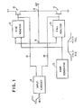
- FIG. 1 is a schematic block diagram of an off-chip driver circuit according to the principles of the present invention.
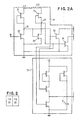
- FIG. 2 is a more detailed schematic circuit of the off-chip driver circuit of FIG. 1.
- FIG. 1 A schematic block diagram of the off-chip driver (OCD) circuit of the present invention is shown in FIG. 1.
- the circuit includes a first output device 10 and a second output device 12 having a common output connection 14.
- a rising (1 bit) or falling (0 bit) signal is applied to an input circuit 8 to provide enabling signals to output devices 10 and 12.
- the output signal which appears at output connection 14, as well as at node 16 exhibits a rise slope di/dt, a rise time t r , a fall slope di/dt and a fall time t f associated with the rise and fall of the input signal.
- a first monitoring device 18 is connected to the output signal at node 16 to monitor the rise time t r of the output signal and a second monitoring device 20 is connected to node 16 to monitor the fall time t f of the output signal.
- a ramp generator 22 is provided which generates a reference signal as shown in FIG. 1 which also includes a rise time t r and a fall time t f .
- the two monitor circuits 18 and 20, which operate separately and independently of each other, respectively, compare the rise and fall times of the output signal from node 16 with the reference rise time (in circuit 18) and reference fall time (in circuit 20). If the comparison shows that the rise time of the output signal is faster or slower than the reference signal rise time, a corresponding feedback signal is provided from monitor circuit 18 on lead 24 which controls the output signal. If the output signal has a rise time faster than the t r of the reference signal from generator 22, then the feedback signal on lead 24 reduces the rise time of the output signal. If the rise time signal becomes too slow, then the feedback signal on lead 24 increases the rise time of the output signal. The same operation occurs with a feedback signal on lead 26 from monitor circuit 20 for the fall time.
- FIG. 1 The circuit of FIG. 1 is more clearly shown in FIG. 2 wherein the same functional elements have been designated by the same reference numbers.
- an input signal is applied to input circuit 8 which signal may have a rising or a falling slope. The case of a rising signal will be discussed first.
- device 28 is on (closed) so that the signal on lead 24 is clamped to ground and device 10 is kept inactive or off.
- the rising input signal is applied to device 30 which operates to pull down the signal on node 32 which is also connected to depletion device 31, such that the input signal is inverted and the input to device 28 falls low.
- the input signal to device 44 obtained from node 33 connected between device 35 and depletion device 37, follows the input signal and rises. This turns off (i.e., opens) device 28, releasing or unclamping lead 24.
- the output signal from output terminal 34 is initially at zero voltage level as is the reference ramp signal from the output of ramp generator 22 which is connected to the device 36 in rise monitor 18.
- the zero voltage level at device 36 causes the signal on lead 38 on the gate of device 40 to be high and the signal on lead 42 to be low.
- Ramp generator 22 is a conventional signal generator responsive to the inverted form of the input signal from node 32. Ramp generator 22 is also responsive to the re-inverted signal which was applied to device 44 such that by operation of the devices charging and discharging capacitor 6, a ramp signal is generated having selected rising and falling portions with predetermined rise and fall times as shown in FIG. 1.
- the output signal (present at node 14 which is connected to device 36 in rise monitor 18) rises faster than the reference ramp signal which is applied to the gate of device 36, the signal on lead 38 goes higher, the signal on lead 42 goes lower, which in turn causes device 10 to conduct less (slow up) and the rise time of the output signal at node 14 slows up, thereby tracking the rise time of the reference ramp signal from generator 22.
- the ramp output signal from generator 22 will rise higher (i.e., +5 volts) than the maximum rise of the output signal on node 14 and output terminal 34 (i.e., +3 volts), and when the ramp signal exceeds the output signal (i.e., +3) then lead 38 of the rise monitor 18 is low and lead 42 gradually rises, leaving device 10 on.
- the signal on node 32 goes up (inverts to input signal) and signal applied to device 44 goes down.
- Device 44 goes off (i.e., opens) which releases or unclamps lead 26, permitting device 12 to operate.
- the output signal on output terminal 34 and node 16 is initially at a raised level (i.e., +3 previously mentioned) and the ramp signal from generator 22 is higher (i.e., +5 previously mentioned).
- the output signal from node 16 and the ramp signal from generator 22 are applied to device 46 of fall monitor 22, therefore, lead 48 is high and lead 50 is low.
- the output signal on node 14 (and output terminal 34) is also connected to the input to device 46 of fall monitor 22, and if it falls faster than the reference ramp signal applied to device 46 from generator 22, then the signal on lead 48 goes high, the signal on lead 50 goes low, the conduction of devices 12 slows, and the fall time of the output signal is made slower.
- the circuit of FIG. 2 not only controls the waveshape of the rise and fall ramps of the circuit output signal (the di/dt), but since the feedback control is obtained from the output lead, any reflections back from the output devices (the transmission lines) which tend to change the output signal rise and fall are also compensated.
Landscapes
- Physics & Mathematics (AREA)
- Engineering & Computer Science (AREA)
- Computer Hardware Design (AREA)
- Computing Systems (AREA)
- General Engineering & Computer Science (AREA)
- Mathematical Physics (AREA)
- Logic Circuits (AREA)
- Electronic Switches (AREA)
Description
- The present invention relates to a driver circuit for controlling signal rise and fall in Field Effect Transistor (FET) circuits, and has particular relevance to a line driver circuit for reducing off-chip electrical disturbances in FET processor by controlling the rise time and fall time of input signals.
- Circuits are available in the prior art which attempt to control signal rise time. In US-A 4132906 issued January 2, 1979 to Allen, entitled CIRCUIT TO IMPROVE RISE TIME AND/OR REDUCE PARASITIC POWER SUPPLY SPIKE CURRENT IN BIPOLAR TRANSISTOR LOGIC CIRCUITS, an improvement in output rise time and a reduction in the parasitic power supply strike current is achieved in bipolar transistor logic circuits using an AC coupled feedback circuit. During the low to high transition of the output, an internal voltage is AC coupled to an amplifier which in turn provides a low impedance path at the base of a lower output drive transistor which is coming out of conduction.
- In this patent, a dual (upper and lower) transistor push-pull output drive stage for a bipolar transistor logic circuit is described. Under low capacitance load conditions, a fast transient voltage occurs on the collector of the lower transistor. Thus a large amount of current is coupled into the base of the transistor while it is coming out of conduction. This current into the base of the lower output transistor will tend to turn the transistor back on so that for a period of time both the upper and lower output driver transistors are carrying current directly from the power supply through the two transistors to ground. As a result there may be current spikes drawn from the power supply which in turn waste power and introduce noise into the rest of the system.
- Thus, to avoid the spike between the output transistors during turn-on, an uncontrolled feedback signal is coupled to the in-phase signal to turn off the lower transistor. This circuit only speeds up the turn-off time of the device, and actually increases the di/dt of the turn-off device.
- In US-A-3436563 issued April 1, 1969 to Regitz entitled PULSE DRIVER WITH LINEAR CURRENT RISE, a pulse driver circuit is described wherein the emitter circuit of the output transistor includes a resistor and inductor in series. Two feedback transistors provide variable shunts of the input drive pulses. One, driven by the voltage across the inductor, limits the rate of increase of output current to a constant value. The second, driven by the voltage across the inductor and resistor, limits the output pulse amplitude to a constant value.
- In this circuit, the obtaining of a feedback signal from an inductance requires an undesirably high voltage and results in a linear ramp (di/dt) of current which is not suitable for off-chip drivers. This circuit also only deals with turn-on, not turn-off.
- In US-A-3914623 issued October 21, 1975 to Clancy entitled WAVEFORM GENERATOR INCLUDING MEANS FOR AUTOMATIC SLOPE CALIBRATION, a waveform generator such as a sawtooth wave generator is described wherein automatic slope calibration is provided. A variable resistance element is feedback-responsive and provides an input voltage which affects waveform shape. The shape of the waveform is controlled automatically by a time error signal through the use of a feedback loop which controls the input voltage.
- FET microprocessor technology is continually improving in both speed and packing density, leading to more circuits per chip and reduced cycle time. This combination gives rise to electrical disturbance problems because of the imperfections of the electrical package. To overcome these difficulties, chip-to-chip signalling through the package is usually done with specially designed off-chip-drivers (OCD) and off-chip-receivers (OCR). The present invention provides a new type of improved OCD to deal with these problems.
- Electrical disturbances occurring off-chip, and caused by the electrical package, could cause sufficient noise so that some latch on a chip will be inadvertently switched, causing an intermittent failure of the circuitry.
- Disturbances considered in the present invention include those due to the products of the mutual and self inductances of the circuit with the rate of change of the current, di/dt, and reflections from the transmission line.
- Normally, an OCD is designed to operate over a wide range of output loads. The output signal traverses a worst case path which has a total capacitance that must be charged and discharged to some level in an acceptable time. The size of the two usual output devices are determined from this criteria. The internal delay of the OCD adds to this external interval, giving an overall delay for worst case (large) load. Parameter variations due to the manufacturing process are included. For output loads which are smaller, the excess drive capacity of the two output devices cause faster outputs. Ideally, top current and bottom current never occur at the same instant. The peak value of output current as well as the di/dt of this current are kept as small as possible. Properly designed, the capacitive load and overall delay are traded off for peak current and large di/dt. Otherwise, a large di/dt will result.
- Treating the OCD load as capacitive is an excellent approximation for previous speeds. As the combination of density and machine cycle, the individual reflections are not merged and the capacitance approximation no longer works.
- Also in an OCD, care must be exercised in treating the output load as capacitive. Part of the load is due to transmission lines and the reflections almost always occur since the terminating impedance never matches the transmission line impedance in FET as machine cycle time gets smaller and OCD speed goes up.
- Thus, an object of the present invention is to provide a driver circuit for reducing off-chip electrical disturbances in an FET processor.
- Another object of the present invention is to provide an off-chip driver circuit for FET processors using feedback signals to control the rise and fall times of the driver output signals.
- Still another object of the present invention is to provide an off-chip driver circuit for FET processors incorporating control means for comparing the driver output signal rise and fall times to a reference signal and for providing a feedback signal therefrom to control the rise and fall time of the driver output signal.
- A still further object of the present invention is to provide an off-chip driver circuit for FET processors that significantly reduces signal rise and fall di/dt problems.
- A further object of the present invention is to provide an off-chip driver circuit wherein output signal rise and fall characteristics are compared to a preselected signal rise and fall standard monitor.
- A still further object of the present invention is to provide an off-chip driver circuit for FET processors that dynamically matches the transmission line Zo, thereby reducing reflections on the drive side. The foregoing and other objects, features and advantages of this invention will be apparent from the following more particular description of the invention, as illustrated in the accompanying drawings.
- FIG. 1 is a schematic block diagram of an off-chip driver circuit according to the principles of the present invention.
- FIG. 2 is a more detailed schematic circuit of the off-chip driver circuit of FIG. 1.
- A schematic block diagram of the off-chip driver (OCD) circuit of the present invention is shown in FIG. 1.
- The circuit includes a
first output device 10 and asecond output device 12 having acommon output connection 14. A rising (1 bit) or falling (0 bit) signal is applied to aninput circuit 8 to provide enabling signals tooutput devices - The output signal which appears at
output connection 14, as well as atnode 16, exhibits a rise slope di/dt, a rise time tr, a fall slope di/dt and a fall time tf associated with the rise and fall of the input signal. - A
first monitoring device 18 is connected to the output signal atnode 16 to monitor the rise time tr of the output signal and asecond monitoring device 20 is connected tonode 16 to monitor the fall time tf of the output signal. - A
ramp generator 22 is provided which generates a reference signal as shown in FIG. 1 which also includes a rise time tr and a fall time tf. - The two
monitor circuits node 16 with the reference rise time (in circuit 18) and reference fall time (in circuit 20). If the comparison shows that the rise time of the output signal is faster or slower than the reference signal rise time, a corresponding feedback signal is provided frommonitor circuit 18 onlead 24 which controls the output signal. If the output signal has a rise time faster than the tr of the reference signal fromgenerator 22, then the feedback signal onlead 24 reduces the rise time of the output signal. If the rise time signal becomes too slow, then the feedback signal onlead 24 increases the rise time of the output signal. The same operation occurs with a feedback signal onlead 26 frommonitor circuit 20 for the fall time. Thus, larger rise and fall times lead to smaller di/dt and the output waveform is independent of the load devices. Furthermore, any reflections or distortions occurring on the output line which tend to change the rise or fall times of the driver will be compensated for because the comparison with the reference signal is made with the signal on the output line. - The circuit of FIG. 1 is more clearly shown in FIG. 2 wherein the same functional elements have been designated by the same reference numbers. As previously stated, an input signal is applied to input
circuit 8 which signal may have a rising or a falling slope. The case of a rising signal will be discussed first. - Initially,
device 28 is on (closed) so that the signal onlead 24 is clamped to ground anddevice 10 is kept inactive or off. The rising input signal is applied todevice 30 which operates to pull down the signal onnode 32 which is also connected todepletion device 31, such that the input signal is inverted and the input todevice 28 falls low. The input signal todevice 44, obtained fromnode 33 connected betweendevice 35 anddepletion device 37, follows the input signal and rises. This turns off (i.e., opens)device 28, releasing or unclampinglead 24. The output signal fromoutput terminal 34 is initially at zero voltage level as is the reference ramp signal from the output oframp generator 22 which is connected to the device 36 in rise monitor 18. The zero voltage level at device 36 causes the signal onlead 38 on the gate ofdevice 40 to be high and the signal onlead 42 to be low. -
Ramp generator 22 is a conventional signal generator responsive to the inverted form of the input signal fromnode 32.Ramp generator 22 is also responsive to the re-inverted signal which was applied todevice 44 such that by operation of the devices charging and discharging capacitor 6, a ramp signal is generated having selected rising and falling portions with predetermined rise and fall times as shown in FIG. 1. - As the ramp signal from generator 22 (applied to the gate of device 36 in monitor 18) rises, the signal on
lead 38 goes low and the signal onlead 42 rises.Device 44 is on, and thelead 26 is clamped to ground.Lead 42 is connected todevice 10 sodevice 10 turns on, raising the signal onoutput lead node 14, thereby producing a rising output signal atoutput terminal 34. - If the output signal (present at
node 14 which is connected to device 36 in rise monitor 18) rises faster than the reference ramp signal which is applied to the gate of device 36, the signal onlead 38 goes higher, the signal onlead 42 goes lower, which in turn causesdevice 10 to conduct less (slow up) and the rise time of the output signal atnode 14 slows up, thereby tracking the rise time of the reference ramp signal fromgenerator 22. - The ramp output signal from
generator 22 will rise higher (i.e., +5 volts) than the maximum rise of the output signal onnode 14 and output terminal 34 (i.e., +3 volts), and when the ramp signal exceeds the output signal (i.e., +3) then lead 38 of the rise monitor 18 is low and lead 42 gradually rises, leavingdevice 10 on. - In the case of a falling input signal to
device 30 ofinput circuit 8, the signal onnode 32 goes up (inverts to input signal) and signal applied todevice 44 goes down.Device 44 goes off (i.e., opens) which releases orunclamps lead 26, permittingdevice 12 to operate. The output signal onoutput terminal 34 andnode 16 is initially at a raised level (i.e., +3 previously mentioned) and the ramp signal fromgenerator 22 is higher (i.e., +5 previously mentioned). The output signal fromnode 16 and the ramp signal fromgenerator 22 are applied todevice 46 of fall monitor 22, therefore, lead 48 is high and lead 50 is low. - As the ramp signal from
generator 22 falls, lead 48 goes low and lead 50 goes up. When the value of the ramp signal goes below the output signal,device 46 opens and lead 48 goes low,device 52 opens and lead 50 goes up. Sincelead 50 is connected todevice 12,device 12 turns on (closes) and pulls the voltage level ofnode 14 down (falls). - The output signal on node 14 (and output terminal 34) is also connected to the input to
device 46 of fall monitor 22, and if it falls faster than the reference ramp signal applied todevice 46 fromgenerator 22, then the signal onlead 48 goes high, the signal onlead 50 goes low, the conduction ofdevices 12 slows, and the fall time of the output signal is made slower. - If the output signal falls slower than the ramp generator signal, a converse feedback operation occurs, wherein
lead 50 goes up,device 12 conducts faster and the output signal falls faster. - Thus, the circuit of FIG. 2 not only controls the waveshape of the rise and fall ramps of the circuit output signal (the di/dt), but since the feedback control is obtained from the output lead, any reflections back from the output devices (the transmission lines) which tend to change the output signal rise and fall are also compensated.
- The embodiment of concepts of the present invention was shown and described as an NMOS FET structure. Another embodiment of the invention may be provided on CMOS using routine design techniques.
Claims (4)
- A driver circuit for providing an output signal having a rise time adjusted in accordance with a rise time of a standard ramp signal ,comprising:an input circuit (8) responsive to an input signal of the type having a rising level, said input circuit providing a corresponding rising signal on an output lead therefrom,an output circuit including at least one output device (10,12) having an output connection (14), said at least one output device being connected to said output lead of said input circuit and responsive to said corresponding rising signal of said input circuit,a ramp generator circuit (22) connected to said output lead of said input circuit for providing an output signal having a desired rise time in response to said corresponding rising signal on said input circuit output lead,a monitor circuit (18,20) connected to said output connection of said at least one output device and to said ramp generator and responsive to said signals thereon to provide a feedback signal to said at least one output device when said output signal rises faster or slower than said ramp signal, said feedback signal adjusting said output signal in accordance with the rise time of said ramp signal.
- A driver circuit according to Claim 1 for providing an output signal having rise times and fall times adjusted in accordance with rise and fall times of a standard ramp signal whereinsaid input circuit is responsive to an input signal of the type having rising and falling signal levels, said input circuit providing a corresponding rising signal on a first output lead and a corresponding falling signal on a second output lead,said output circuit includes first and second output devices having a common output connection, said first output device being connected to said first output lead of said input circuit and responsive to said rising signal of said input circuit and said second output device being connected to said second output lead of said input circuit and responsive to said falling signal of said input circuit,said ramp generator circuit is connected to said first and second output leads of said input circuit for providing an output signal having desired rise and fall times in response to said rising and falling signals on said input circuit output leads,said monitor circuit is a first monitor circuit (18) and is connected to said common output connection of said first and second output devices and to said ramp generator and is responsive to said signals thereon to provide a feedback signal to said first output device when said output signal rises faster or slower than said ramp signal, said feedback signal adjusting said output signal in accordance with the rise time of said ramp signal,and wherein said driver circuit further includes a second monitor circuit (20) connected to said ramp generator and said common output connection of said first and second output devices and is responsive to the signals therefrom to provide a feedback signal to said second output device when said output signal falls faster or slower than said ramp signal, said feedback signal adjusting said output signal in accordance with the fall time of said ramp signal.
- A driver circuit according to Claim 2 wherein said first monitor circuit includes a first transistor device (36) connected to the output of said ramp generator circuit for providing an opposite, falling signal in response to said rising signal from said ramp generator circuit, a second transistor device (40) connected to said first transistor device for producing a rising signal in response to said falling signal from said first transistor, said rising signal from said second transistor being electrically connected to said first output device to produce a rising signal on said common output connection,and wherein said common output connection is electrically connected to said first transistor device to feedback said signal from said common output connection for controlling the output signal from said first transistor device, such that the said output from said first transistor device and consequently the output from said second transistor device is determined by said ramp generator output signal and said signal on said common output connection.
- A driver circuit according to Claim 3 wherein said second monitor circuit includes a third transistor device (46) connected to the output of said ramp generator circuit for providing an opposite, rising signal in response to said falling signal from said ramp generator circuit, a fourth transistor device (52) connected to said third transistor device for producing a falling signal in response to said rising signal from said third transistor, said falling signal from said fourth transistor being electrically connected to said second output device to produce a falling signal on said common output connection,and wherein said common output connection is electrically connected to said third transistor device to feedback said signal from said common output connection for controlling the output signal from said third transistor device, such that the said output from said third transistor device and consequently the output from said fourth transistor device is determined by said ramp generator output signal and said signal on said common output connection.
Applications Claiming Priority (2)
| Application Number | Priority Date | Filing Date | Title |
|---|---|---|---|
| US620235 | 1984-06-13 | ||
| US06/620,235 US4567378A (en) | 1984-06-13 | 1984-06-13 | Driver circuit for controlling signal rise and fall in field effect transistor processors |
Publications (3)
| Publication Number | Publication Date |
|---|---|
| EP0164615A2 EP0164615A2 (en) | 1985-12-18 |
| EP0164615A3 EP0164615A3 (en) | 1988-04-06 |
| EP0164615B1 true EP0164615B1 (en) | 1991-03-13 |
Family
ID=24485124
Family Applications (1)
| Application Number | Title | Priority Date | Filing Date |
|---|---|---|---|
| EP85106193A Expired EP0164615B1 (en) | 1984-06-13 | 1985-05-21 | Driver circuit for controlling signal rise and fall in field effect transistor circuits |
Country Status (4)
| Country | Link |
|---|---|
| US (1) | US4567378A (en) |
| EP (1) | EP0164615B1 (en) |
| JP (1) | JPS614319A (en) |
| DE (1) | DE3582086D1 (en) |
Families Citing this family (69)
| Publication number | Priority date | Publication date | Assignee | Title |
|---|---|---|---|---|
| JPH0720060B2 (en) * | 1985-08-14 | 1995-03-06 | 株式会社東芝 | Output circuit device |
| US4719369A (en) * | 1985-08-14 | 1988-01-12 | Hitachi, Ltd. | Output circuit having transistor monitor for matching output impedance to load impedance |
| JPS62159917A (en) * | 1986-01-08 | 1987-07-15 | Toshiba Corp | Inverter circuit in integrated circuit |
| JPS62220026A (en) * | 1986-03-20 | 1987-09-28 | Toshiba Corp | Output buffer circuit |
| NL8601558A (en) * | 1986-06-17 | 1988-01-18 | Philips Nv | INTEGRATED LOGIC CIRCUIT PROVIDED WITH AN OUTPUT CIRCUIT FOR GENERATING AN OUTPUT CURRENT IN TIME. |
| JPS635553A (en) * | 1986-06-25 | 1988-01-11 | Fujitsu Ltd | Buffer circuit |
| US4758743A (en) * | 1986-09-26 | 1988-07-19 | Motorola, Inc. | Output buffer with improved di/dt |
| JPS63112893A (en) * | 1986-10-28 | 1988-05-17 | Mitsubishi Electric Corp | Semiconductor integrated circuit |
| US4739193A (en) * | 1986-10-30 | 1988-04-19 | Rca Corporation | Drive circuit with limited signal transition rate for RFI reduction |
| US4704550A (en) * | 1986-11-07 | 1987-11-03 | American Telephone And Telegraph Company | Method and apparatus for driving electrical circuits |
| US4785201A (en) * | 1986-12-29 | 1988-11-15 | Integrated Device Technology, Inc. | High speed/high drive CMOS output buffer with inductive bounce suppression |
| JPS63234623A (en) * | 1987-03-23 | 1988-09-29 | Toshiba Corp | Semiconductor integrated circuit |
| JPS63240128A (en) * | 1987-03-27 | 1988-10-05 | Toshiba Corp | logic circuit |
| KR880013321A (en) * | 1987-04-07 | 1988-11-30 | 언윈 엘. 콰텍 | Method and apparatus for reducing transient noise in integrated circuits |
| WO1988008228A2 (en) * | 1987-04-07 | 1988-10-20 | Western Digital Corporation | Method and apparatus for reducing transient noise in integrated circuits |
| US4752703A (en) * | 1987-04-23 | 1988-06-21 | Industrial Technology Research Institute | Current source polarity switching circuit |
| US4823029A (en) * | 1987-06-25 | 1989-04-18 | American Telephone And Telegraph Company At&T Bell Laboratories | Noise controlled output buffer |
| AU608822B2 (en) * | 1987-06-29 | 1991-04-18 | Digital Equipment Corporation | Bus transmitter having controlled trapezoidal slew rate |
| US5070256A (en) * | 1987-06-29 | 1991-12-03 | Digital Equipment Corporation | Bus transmitter having controlled trapezoidal slew rate |
| US4818901A (en) * | 1987-07-20 | 1989-04-04 | Harris Corporation | Controlled switching CMOS output buffer |
| US4797579A (en) * | 1987-07-27 | 1989-01-10 | Raytheon Company | CMOS VLSI output driver with controlled rise and fall times |
| JPH0799639B2 (en) * | 1987-07-31 | 1995-10-25 | 株式会社東芝 | Semiconductor integrated circuit |
| US4800298A (en) * | 1987-08-04 | 1989-01-24 | Motorola, Inc. | Output buffer for improving di/dt |
| US4777389A (en) * | 1987-08-13 | 1988-10-11 | Advanced Micro Devices, Inc. | Output buffer circuits for reducing ground bounce noise |
| US4859870A (en) * | 1987-10-14 | 1989-08-22 | Lsi Logic Incorporated | Two-mode driver circuit |
| WO1989003614A1 (en) * | 1987-10-14 | 1989-04-20 | Lsi Logic Corporation | Two-mode driver circuit |
| US4862018A (en) * | 1987-11-30 | 1989-08-29 | Texas Instruments Incorporated | Noise reduction for output drivers |
| US4855622A (en) * | 1987-12-18 | 1989-08-08 | North American Philips Corporation, Signetics Division | TTL compatible switching circuit having controlled ramp output |
| US4825101A (en) * | 1988-02-11 | 1989-04-25 | Advanced Micro Devices, Inc. | Full-level, fast CMOS output buffer |
| JPH01238217A (en) * | 1988-03-18 | 1989-09-22 | Toshiba Corp | Malfunction preventing circuit for semiconductor integrated circuit |
| US4862020A (en) * | 1988-06-20 | 1989-08-29 | Tektronix, Inc. | Electronic delay control circuit having pulse width maintenance |
| JPH0666674B2 (en) * | 1988-11-21 | 1994-08-24 | 株式会社東芝 | Output circuit of semiconductor integrated circuit |
| US5010256A (en) * | 1989-02-21 | 1991-04-23 | United Technologies Corporation | Gate output driver using slew-rate control |
| US4962344A (en) * | 1989-05-23 | 1990-10-09 | Advanced Micro Devices, Inc. | Segmented waveform generator |
| US5216294A (en) * | 1989-05-31 | 1993-06-01 | Samsung Electronics Co., Ltd. | Data output buffer using a junction field effect transistor |
| US4963765A (en) * | 1989-07-03 | 1990-10-16 | Texas Instruments Incorporated | High speed CMOS transition detector circuit |
| US4996499A (en) * | 1989-09-15 | 1991-02-26 | Delco Electronics Corporation | Amplitude stabilized oscillator amplifier |
| US4972101A (en) * | 1989-09-19 | 1990-11-20 | Digital Equipment Corporation | Noise reduction in CMOS driver using capacitor discharge to generate a control voltage |
| US5015880A (en) * | 1989-10-10 | 1991-05-14 | International Business Machines Corporation | CMOS driver circuit |
| US5164611A (en) * | 1990-10-18 | 1992-11-17 | Delco Electronics Corporation | Low noise communication bus driver |
| IT1246755B (en) * | 1990-12-28 | 1994-11-26 | Sgs Thomson Microelectronics | FAST PILOTING CIRCUIT OF A CAPACITIVE LOAD FOR INTEGRAL CIRCUITS, PARTICULARLY MEMORIES. |
| JP3014164B2 (en) * | 1991-05-15 | 2000-02-28 | 沖電気工業株式会社 | Output buffer circuit |
| US5311084A (en) * | 1992-06-23 | 1994-05-10 | At&T Bell Laboratories | Integrated circuit buffer with controlled rise/fall time |
| US5369317A (en) * | 1992-06-26 | 1994-11-29 | Micron Technology, Inc. | Circuit and method for controlling the potential of a digit line and in limiting said potential to a maximum value |
| US5315187A (en) * | 1992-08-05 | 1994-05-24 | Acer Incorporated | Self-controlled output stage with low power bouncing |
| GB9217994D0 (en) * | 1992-08-24 | 1992-10-07 | Immos Limited | Improvements in or relating to ic output drivers |
| US5657456A (en) * | 1993-06-18 | 1997-08-12 | Digital Equipment Corporation | Semiconductor process power supply voltage and temperature compensated integrated system bus driver rise and fall time |
| US5414312A (en) * | 1993-07-15 | 1995-05-09 | Altera Corporation | Advanced signal driving buffer with directional input transition detection |
| KR970005570B1 (en) * | 1994-07-14 | 1997-04-17 | 현대전자산업 주식회사 | Data output buffer |
| US5642274A (en) * | 1994-07-26 | 1997-06-24 | U.S. Philips Corporation | Low noise sinusoidal controller for pulse width modulated converters |
| JP2655096B2 (en) * | 1994-09-29 | 1997-09-17 | 日本電気株式会社 | Output buffer circuit |
| US5598119A (en) * | 1995-04-05 | 1997-01-28 | Hewlett-Packard Company | Method and apparatus for a load adaptive pad driver |
| WO1997012443A1 (en) * | 1995-09-26 | 1997-04-03 | Philips Electronics N.V. | Pre-regulator with active current limiting for power transistor |
| US6014046A (en) * | 1997-07-31 | 2000-01-11 | International Business Machines Corporation | Off chip driver (OCD) with variable drive capability for noise control |
| US6040707A (en) * | 1997-09-15 | 2000-03-21 | Intersil Corporation | Constant slew rate amplifier |
| US6114895A (en) * | 1997-10-29 | 2000-09-05 | Agilent Technologies | Integrated circuit assembly having output pads with application specific characteristics and method of operation |
| US6157204A (en) | 1998-08-05 | 2000-12-05 | Micron Technology, Inc. | Buffer with adjustable slew rate and a method of providing an adjustable slew rate |
| EP1264401B9 (en) * | 2000-01-20 | 2004-03-03 | Infineon Technologies AG | Arrangement and method for adjusting the slope times of one or more drivers and a driver circuit |
| US6313664B1 (en) * | 2000-03-20 | 2001-11-06 | Motorola Inc. | Load capacitance compensated buffer, apparatus and method thereof |
| DE10034713A1 (en) * | 2000-07-17 | 2002-02-07 | Infineon Technologies Ag | Method and device for assessing the strength of a driver |
| US6670683B2 (en) | 2001-01-04 | 2003-12-30 | International Business Machines Corporation | Composite transistor having a slew-rate control |
| US7038513B2 (en) * | 2004-06-29 | 2006-05-02 | Intel Corporation | Closed-loop independent DLL-controlled rise/fall time control circuit |
| DE102004036958A1 (en) * | 2004-07-30 | 2006-03-23 | Tridonicatco Gmbh & Co. Kg | Control of circuit breakers |
| KR100666931B1 (en) * | 2004-12-28 | 2007-01-10 | 주식회사 하이닉스반도체 | Semiconductor memory device |
| FR2897993A1 (en) | 2006-02-28 | 2007-08-31 | Atmel Nantes Sa Sa | ELECTRONIC DEVICE FOR CONTROLLING AN EXTERNAL LOAD WHOSE OUTPUT SIGNAL SLOPE IS INDEPENDENT OF THE EXTERNAL LOAD CAPACITY AND CORRESPONDING INTEGRATED COMPONENT |
| ATE455395T1 (en) | 2006-08-08 | 2010-01-15 | Semiconductor Components Ind | DRIVER CIRCUIT |
| EP2211464A1 (en) * | 2009-01-26 | 2010-07-28 | Siemens Aktiengesellschaft | Communications switch and communications method |
| EP3319274B1 (en) * | 2016-11-02 | 2019-04-17 | NXP USA, Inc. | Can module and method therefor |
| US10892760B1 (en) * | 2019-10-15 | 2021-01-12 | Qualcomm Incorporated | Dynamic transistor gate overdrive for input/output (I/O) drivers and level shifters |
Family Cites Families (20)
| Publication number | Priority date | Publication date | Assignee | Title |
|---|---|---|---|---|
| US3436563A (en) * | 1965-12-27 | 1969-04-01 | Bell Telephone Labor Inc | Pulse driver with linear current rise |
| US3535555A (en) * | 1968-07-26 | 1970-10-20 | Us Navy | Ramp function generator having voltage controlled slope |
| DE2001003A1 (en) * | 1970-01-10 | 1971-07-15 | Zuse Kg | Arrangement for generating voltage pulses |
| US3714466A (en) * | 1971-12-22 | 1973-01-30 | North American Rockwell | Clamp circuit for bootstrap field effect transistor |
| GB1424525A (en) * | 1972-05-11 | 1976-02-11 | Elliott Brothers London Ltd | Data transmission system |
| GB1451732A (en) * | 1973-03-19 | 1976-10-06 | Motorola Inc | Signal shaping circuit |
| US3914623A (en) * | 1973-10-31 | 1975-10-21 | Westinghouse Electric Corp | Waveform generator including means for automatic slope calibration |
| US3973145A (en) * | 1974-01-14 | 1976-08-03 | King Radio Corporation | Weather radar transistorized pulse modulator |
| US3906254A (en) * | 1974-08-05 | 1975-09-16 | Ibm | Complementary FET pulse level converter |
| JPS51105752A (en) * | 1975-03-14 | 1976-09-18 | Hitachi Ltd | PARUSUDENATSU HATSUSEIYODENSHIKAIRO |
| US4029972A (en) * | 1975-12-16 | 1977-06-14 | Westinghouse Electric Corporation | Ramping circuit |
| JPS5917765B2 (en) * | 1976-09-13 | 1984-04-23 | 石川島播磨重工業株式会社 | Single pulse generation method |
| US4132906A (en) * | 1977-02-28 | 1979-01-02 | Motorola, Inc. | Circuit to improve rise time and/or reduce parasitic power supply spike current in bipolar transistor logic circuits |
| US4216393A (en) * | 1978-09-25 | 1980-08-05 | Rca Corporation | Drive circuit for controlling current output rise and fall times |
| US4250410A (en) * | 1979-02-27 | 1981-02-10 | Motorola, Inc. | Speed-up circuit |
| IE49593B1 (en) * | 1979-05-18 | 1985-10-30 | Gen Electric Co Ltd | Transistor switching circuit |
| US4329600A (en) * | 1979-10-15 | 1982-05-11 | Rca Corporation | Overload protection circuit for output driver |
| US4314166A (en) * | 1980-02-22 | 1982-02-02 | Rca Corporation | Fast level shift circuits |
| US4359650A (en) * | 1980-11-13 | 1982-11-16 | The United States Of America As Represented By The Secretary Of The Air Force | High voltage driver amplifier apparatus |
| US4527081A (en) * | 1983-02-11 | 1985-07-02 | The United States Of America As Represented By The Scretary Of The Army | Overshoot predriven semi-asynchronous driver |
-
1984
- 1984-06-13 US US06/620,235 patent/US4567378A/en not_active Expired - Lifetime
-
1985
- 1985-01-31 JP JP60015638A patent/JPS614319A/en active Pending
- 1985-05-21 DE DE8585106193T patent/DE3582086D1/en not_active Expired - Lifetime
- 1985-05-21 EP EP85106193A patent/EP0164615B1/en not_active Expired
Also Published As
| Publication number | Publication date |
|---|---|
| DE3582086D1 (en) | 1991-04-18 |
| EP0164615A2 (en) | 1985-12-18 |
| US4567378A (en) | 1986-01-28 |
| EP0164615A3 (en) | 1988-04-06 |
| JPS614319A (en) | 1986-01-10 |
Similar Documents
| Publication | Publication Date | Title |
|---|---|---|
| US4567378A (en) | Driver circuit for controlling signal rise and fall in field effect transistor processors | |
| US11594970B2 (en) | Overcurrent protection based on zero current detection | |
| EP0284356B1 (en) | A data output circuit | |
| US6380796B2 (en) | Semiconductor power converting apparatus | |
| US5321319A (en) | High speed CMOS bus driver circuit that provides minimum output signal oscillation | |
| US4656369A (en) | Ring oscillator substrate bias generator with precharge voltage feedback control | |
| US4504779A (en) | Electrical load drive and control system | |
| US10236877B1 (en) | Power transistor control signal gating | |
| EP0329285B1 (en) | Output buffer | |
| US4758743A (en) | Output buffer with improved di/dt | |
| EP0557080B1 (en) | Output buffer with controlled output level | |
| EP0574184B1 (en) | High speed CMOS output buffer circuits | |
| EP0097889B1 (en) | Driver circuit with means for reducing self-induced switching noise | |
| JPH04172962A (en) | IGBT drive circuit | |
| EP0799528B1 (en) | Negative feedback to reduce voltage oscillation in cmos output buffers | |
| US4684824A (en) | Capacitive load driver circuit | |
| JP4091793B2 (en) | Gate drive circuit of voltage driven semiconductor device | |
| US4896244A (en) | Feed forward compensation circuitry and switching logic driver with overcurrent protection incorporating same | |
| CN108683329A (en) | A kind of load current real-time detection system | |
| US4924120A (en) | Low noise output circuit | |
| US5089721A (en) | Ground bounce isolation and high speed output circuit | |
| EP0928066B1 (en) | Circuit to steepen pulse edges | |
| US4639823A (en) | Control circuit for switching transistors | |
| US4906866A (en) | Output buffer for improving di/dt | |
| US4890015A (en) | Method and circuitry for controlling the compensation of negative internal ground voltage fluctuations |
Legal Events
| Date | Code | Title | Description |
|---|---|---|---|
| PUAI | Public reference made under article 153(3) epc to a published international application that has entered the european phase |
Free format text: ORIGINAL CODE: 0009012 |
|
| AK | Designated contracting states |
Designated state(s): DE FR GB |
|
| 17P | Request for examination filed |
Effective date: 19860424 |
|
| PUAL | Search report despatched |
Free format text: ORIGINAL CODE: 0009013 |
|
| AK | Designated contracting states |
Kind code of ref document: A3 Designated state(s): DE FR GB |
|
| 17Q | First examination report despatched |
Effective date: 19891213 |
|
| GRAA | (expected) grant |
Free format text: ORIGINAL CODE: 0009210 |
|
| AK | Designated contracting states |
Kind code of ref document: B1 Designated state(s): DE FR GB |
|
| REF | Corresponds to: |
Ref document number: 3582086 Country of ref document: DE Date of ref document: 19910418 |
|
| ET | Fr: translation filed | ||
| PLBE | No opposition filed within time limit |
Free format text: ORIGINAL CODE: 0009261 |
|
| STAA | Information on the status of an ep patent application or granted ep patent |
Free format text: STATUS: NO OPPOSITION FILED WITHIN TIME LIMIT |
|
| 26N | No opposition filed | ||
| PGFP | Annual fee paid to national office [announced via postgrant information from national office to epo] |
Ref country code: GB Payment date: 19920409 Year of fee payment: 8 |
|
| PGFP | Annual fee paid to national office [announced via postgrant information from national office to epo] |
Ref country code: FR Payment date: 19920427 Year of fee payment: 8 |
|
| PGFP | Annual fee paid to national office [announced via postgrant information from national office to epo] |
Ref country code: DE Payment date: 19920523 Year of fee payment: 8 |
|
| PG25 | Lapsed in a contracting state [announced via postgrant information from national office to epo] |
Ref country code: GB Effective date: 19930521 |
|
| GBPC | Gb: european patent ceased through non-payment of renewal fee |
Effective date: 19930521 |
|
| PG25 | Lapsed in a contracting state [announced via postgrant information from national office to epo] |
Ref country code: FR Effective date: 19940131 |
|
| PG25 | Lapsed in a contracting state [announced via postgrant information from national office to epo] |
Ref country code: DE Effective date: 19940201 |
|
| REG | Reference to a national code |
Ref country code: FR Ref legal event code: ST |