EP0163580A2 - Semiconductor integrated circuit with redundant circuit replacement - Google Patents
Semiconductor integrated circuit with redundant circuit replacement Download PDFInfo
- Publication number
- EP0163580A2 EP0163580A2 EP85401065A EP85401065A EP0163580A2 EP 0163580 A2 EP0163580 A2 EP 0163580A2 EP 85401065 A EP85401065 A EP 85401065A EP 85401065 A EP85401065 A EP 85401065A EP 0163580 A2 EP0163580 A2 EP 0163580A2
- Authority
- EP
- European Patent Office
- Prior art keywords
- circuit
- transistor
- transistors
- circuit according
- address
- Prior art date
- Legal status (The legal status is an assumption and is not a legal conclusion. Google has not performed a legal analysis and makes no representation as to the accuracy of the status listed.)
- Granted
Links
Images


Classifications
-
- G—PHYSICS
- G11—INFORMATION STORAGE
- G11C—STATIC STORES
- G11C29/00—Checking stores for correct operation ; Subsequent repair; Testing stores during standby or offline operation
-
- G—PHYSICS
- G11—INFORMATION STORAGE
- G11C—STATIC STORES
- G11C29/00—Checking stores for correct operation ; Subsequent repair; Testing stores during standby or offline operation
- G11C29/70—Masking faults in memories by using spares or by reconfiguring
- G11C29/78—Masking faults in memories by using spares or by reconfiguring using programmable devices
- G11C29/835—Masking faults in memories by using spares or by reconfiguring using programmable devices with roll call arrangements for redundant substitutions
Definitions
- the present invention relates to an integrated circuit having memory cells.
- the integrated circuit according to the present invention is used for a memory device having a redundant circuit portion for replacing failed circuits.
- an integrated circuit device for a semiconductor memory is provided with "redundant-bit" type memory cells in addition to the usually used memory cells. These are used to replace failed memory cells or even to replace an entire bit line containing failed memory cells, in the latter case by a redundant bit line containing redundant memory cells. This increases the yield of the products in-the manufacture of integrated circuits.
- ROM's read-only memories
- the circuit is switched to access a redundant memory cell instead of the failed memory cell. Accordingly, quick and correct detection of the written state of the ROM's is important.
- a semiconductor integrated circuit including a memory unit for storing address information of a failed circuit portion for replacing the failed circuit portion by a redundant circuit portion; a comparison unit for detecting coincidence between data read from the memory unit and a received input address; and a delivery unit for delivering data obtained from the comparison by the comparison unit through an external connection terminal.
- Fig. 1 is block diagram of a prior art integrated circuit
- the device of Fig. 1 includes coincidence detection circuits 2, 2, ..., corresponding to the number of bits of the input address signals A 0 , A 1 , ... A n , and a depletion type transistor 32 as a load transistor.
- Non-inverted and inverted address signals A 0 , A 0 , A 1 , A 1 , ... An and An are supplied to the coincidence detection circuits 2, 2 ...
- Each of the coincidence detection circuits carries out a comparison between the input address signal and the stored address signal in a ROM in the coincidence detection circuit.
- the potential of the control line 31 (N l ) becomes HIGH, while when one or more of the coincidence detection circuits does not indicate coincidence, the potential of the control line 31 (N 1 ) becomes LOW.
- the ROM's in the coincidence detection circuits store the address of failed memory cell.
- the potential of the control line 31 (N 1 ) becomes HIGH.
- a redundant memory cell is accessed instead of the failed memory cell.
- a fuse 211 and a transistor 213 constitute a fuse blow-out type ROM.
- One bit of the address information of a failed memory cell is stored in this ROM.
- Transistors 231 and 232 constitute an inverter circuit.
- Transistors 241 to 244 constitute a comparison circuit in the form of an exclusvie OR gate circuit. The series-connected transistors 241 and 242 and the series-connected transistors 243 and 244 are connected between the control line 31 (N 1 ) and the voltage source line V ss .
- the gate of the transistor 241 is connected to the output node N 2 of the inverter circuit (231, 232).
- the gate of the transistor 243 is connected to the output node N 3 of the fuse blow-out type ROM (211, 213).
- the non-inverted address signal A is supplied to the gate of the transistor 242, while the inverted address signal A is supplied to the gate of the transistor 244.
- the fuse blow-out type ROM (211, 212) stores the address data "0" by the blown state of the fuse 211 and stores the address date "1" by the non-blown state of the fuse 211.
- the potential of the control line 31 (N 1 ) becomes HIGH.
- Figure 3 shows another example of the structure of the coincidence detection circuits 2, 2, ... shown in Fig. 1.
- the ROM portion of the coincidence detection circuit of Fig. 3 includes a series-connected fuse 211 and a depletion type transistor 213, a series-connected fuse 212 and a depletion type transistor 214, and a NAND gate circuit consisting of a series-connected depletion type transistor 221, enhancement type transistor 222, and enhancement type transistor 223.
- ... A n are changed successively from “0, 0, ... 0" to "1, 1, ... 1", and the values of the address signals which make the potential of the control line 31 (N 1 ) HIGH is inspected.
- the values of the address signals A 0 , A 1 ... A n which make the potential of the control line 13 (N 1 ) HIGH indicate the address of the failed portion.
- FIG. 4 A semiconductor integrated circuit according to an embodiment of the present invention is illustrated in Fig. 4.
- the circuit of Fig. 4 includes coincidence detection circuits 2, 2, ..., a load transistor 32, an output circuit consisting of transistors 61 and 62, and an external connection terminal 7.
- the transistor 32 is connected between a voltage source V cc and the control line 31 (N 1 ) and is operated as a pull-up circuit or a load circuit.
- the transistors 61 and 62 are connected in series between the voltage source V ss and an external connection terminal 7.
- the gate of the transistor 61 is connected with the control line 31 (N 1 ), while the gate of the transistor 62 is connected with the junction of the transistors 61 and 62.
- the external connection terminal 7 may be used also for a terminal for another signal.
- Non-inverted and inverted signals A 0 , A 0 , A 1 , A 1 , ... A n , A n are supplied to the coincidence detection circuit 2, 2, ... in the circuit of Fig. 4.
- the input address signals are compared with the address signals stored in the ROM's in the coincidence detection circuits. When the compared signals coincide, the impedance between the output terminal of the coincidence detection circuit connected with the control line 31 (N 1 ) and the voltage source V ss becomes HIGH. When the compared signals do not coincide, the above-mentioned impedance becomes LOW.
- a redundant memory call is accessed instead of a failed memory cell only when the potential of the control line 31 (N 1 ) is HIGH. Such an arrangement endless automatic switching from the failed memory cell to the redundant memory cell.
- Various tests of the integrated circuit can be carried out conveniently by using the information concerning failed bits stored in the ROM's in the ' coincidence detection circuits.
- the detection of the information stored in the ROM's is carried out by inputting a sequence of varying addressee A 0 , A 1 ... An and detecting sequentially the potentials of the external connection terminal 7 accordingly.
- the indication of a resistor 8 and a voltage source V , for example -3V, in broken lines is for explaining how current flows through the external connection terminal 7 after application of a voltage V x through the resistor 8 to the external connection terminal 7.
- the coincidence detection circuit shown in Fig. 2 is used for each of the coincidence detection circuits 2, 2, ... in the circuit shown in Fig. 4.
- FIG. 5 A semiconductor integrated circuit according to another embodiment of the present invention is illustrated in Fig. 5.
- Each of the coincidence detection circuits 2, 2, ... in the circuit shown in Fig. 5 has two output terminals, one connected with a control line 31 (N 1 ), the other connected with a detection line 4 1 (N 21 ).
- Each of the coincidence detection circuits 2, 2, ... includes a memory portion 21, a comparison portion 24, and a status detection portion 25.
- the structure of the coincidence detection circuit 2 is illustrated in Fig. 6.
- the status detection portion 25 includes transistors 2501 and 2502, which are connected in series between a detection line 41 (N 2l ) and a voltage source V .
- the gate of the transistor 2501 is connected to a node N 3 in the ROM 21.
- the gate of the transistor 2502 receives the input signal A.
- the impedance between the control line 31 (N 1 ) and the voltage source V ss is HIGH when the potentials of the nodes N 3 and N 2 conform to the input signals A and A, while the impedance is LOW when the potentials of the nodes N 3 and N 2 do not conform to the input signal A and A .
- the potential of the input signal A is made HIGH in order to detect the storage state of the ROM 21, that is, the state of the fuse 211.
- the transistor 2502 becomes ON, and the information of the state of the fuse 211 is output to the detection line 41 (N 21).
- the potential of the node N 3 is LOW, and the transistor 2501 becomes OFF. Accordingly, the impedance between the control line 31 (N 1 ) and the voltage source V ss is HIGH. Hence, the potential of the detection line 41 (N 21 ) becomes HIGH due to the operation of the depletion type transistor 42 (Fig. 5) connected between the detection line 41 (N21) and the voltage source V cc , so that the blown state of the fuse 211 is detected.
- FIG. 7 Another example of the structure of the coincidence detection circuit is shown in Fig. 7.
- the circuit of Fig. 7 is similar to the circuit of Fig. 3, except that the status detection circuit 25 consisting of transistors 2503 to 2507 is added.
- a non-inverted selection signal A n+1 and an inverted selection signal A n+1 are applied to the gates of the transistors 2505 and 2507.
- a non-inverted address signal A is applied to the gate of the transistor 2503.
- the address signal A and the non-inverted signals A n+1 are made HIGH. Hence, the transistors 2503 and 2505 becomes ON.
- the address signal A HIGH and the selection signal A n+1 LOW, that is, the selection signal An+, HIGH the information of the state of the fuse 212 is output to the detection line 41 (N 21 ).
- the state of each of the fuses 211 and 212 can be detected separately.
- the circuit of Fig. 7 is particularly useful for the case where the memory cell matrix is divided by rows or by columns to be divided into a plurality of blocks in which the switching to the redundant circuit is carried out simultaneously in parallel with regard to the plurality of blocks.
- the circuit of Fig. 8 includes a status detection circuit 25, consisting of the transistors 2508 to 2511, and detection lines 41 (N21) and 51 (N 31 ).
- Series-connected transistors 2508 and 2509 are connected between the detection line 41 (N 21 ) and the voltage source V ss
- series-connected transistors 2510 and 2511 are connected between the detection line 51 (N 31 ) and the voltage source V ss .
- the gates of the transistors 2508 and 2510 are connected to the nodes N 4 and N 5 .
- the gates of the transistors 2509 and 2511 receive the address signal A.
- the transistors 2509 and 2511 are caused to be ON by making the address signal A high. Under this condition, when the fuse 211 is blown, the potential of the node N 4 is LOW, the transistor 2508 is OFF, and, accordingly, the potential of the detection line 41 (N 21 ) becomes HIGH. When the fuse 211 is not blown, the potential of the node N 4 is HIGH, the transistor 2508 is ON, and, accordingly, the potential of the detection line 41 (N 21 ) becomes LOW.
- the transistor 2510 is OFF, and, accordingly, the potential of the detection line 51 (N 31 ) becomes HIGH.
- the transistor 2510 is ON, and, accordingly, the potential of the detection line 51 (N31) becomes LOW.
- the address signal is increased successively by one bit for detecting the state of the ROM corresponding to each of the bits of the address signal.
- an inverted address signal A instead of a non-inverted address signal A, is supplied to the gate of the transistor 2502, it is possible to detect the state of the fuse 211 by making the address signal A LOW.
- the address signal applied to the transistor 2502 By making the address signal applied to the transistor 2502 to be, bit by bit, a non-inverted address signal or an inverted address signal, it is possible to select any pattern of address signals for detecting the written state of the ROM.
- Table (A) indicates the address signal supplied to the gate of the transistor 2502.
- Table (B) indicates the address pattern for detecting the state of the ROM.
- the circuit of Fig. 9 includes a status detection circuit 25 consisting of transistors 2512, 2521, 2522, ... 252k.
- the gate of the transistor 2512 receives the potential of the node N 3 which represent the state of the fuse 211.
- the gates of the transistors 2521, 2522, ... 252k receive either one of the non-inverted signals A (A 0 , A 1 , ... An) or one of the inverted signals A ( A 0 , A 1 , ... A n ) of the corresponding bit of the input address.
- 2 k+1 status detection circuits can be realized so that the detection of the states of 2 k+1 fuses can be carried out.
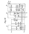
- FIG. 10 A further example of the structure of the coincidence detection circuit is shown in Fig. 10.
- the circuit of Fig. 10 includes a status detection circuit 25 consisting of transistors 2531, 2532, 2541a, 2541b, 2542, 2543, ... 254k.
- the operation of the circuit of Fig. 10 will be apparent from the operations of the circuit of Fig. 7 and the circuit of Fig. 9.
Abstract
Description
- The present invention relates to an integrated circuit having memory cells. The integrated circuit according to the present invention is used for a memory device having a redundant circuit portion for replacing failed circuits.
- In general, an integrated circuit device for a semiconductor memory is provided with "redundant-bit" type memory cells in addition to the usually used memory cells. These are used to replace failed memory cells or even to replace an entire bit line containing failed memory cells, in the latter case by a redundant bit line containing redundant memory cells. This increases the yield of the products in-the manufacture of integrated circuits.
- In such an integrated circuit, read-only memories (ROM's) are provided for storing the addresses of the failed memory cells. When an input address signal coincides with the address of a failed memory cell stored in the ROM's, the circuit is switched to access a redundant memory cell instead of the failed memory cell. Accordingly, quick and correct detection of the written state of the ROM's is important.
- However, 2n+l cycles are usually required for detecting the written state of the ROM's. Hence, a very long time is required for testing an integrated circuit.
- Also, when several fuses are used for each bit in the ROM's, it is impossible to determine the blow-out state of each of the fuses, although the output state of the ROM's can be determined. This is undesirable and causes problems in an integrated circuit device for a semiconductor memory.
- It is an object of the present invention to provide an improved integrated circuit having memory cells, enabling quick and correct detection of the written state of the memory circuit in which the address information of the failed circuit portions is stored, and easy, reliable inspection of the integrated circuit having regular memory cells and redundant circuits without providing an additional external connection terminal of the integrated circuit.
- It is thus another object of the present invention to reduce the time required for the testing of an integrated circuit having regular memory cells and redundant circuits.
- It is still another object of the present invention to enable detection of the blow-out state of each of the plurality of fuses used in the memory cells in the integrated circuit.
- According to the present invention, there is provided a semiconductor integrated circuit including a memory unit for storing address information of a failed circuit portion for replacing the failed circuit portion by a redundant circuit portion; a comparison unit for detecting coincidence between data read from the memory unit and a received input address; and a delivery unit for delivering data obtained from the comparison by the comparison unit through an external connection terminal.
- In the drawings. Fig. 1 is block diagram of a prior art integrated circuit;
- Figs. 2 and 3 show examples of the structure of the coincidence detection circuit used in the circuit shown in Fig. 1;
- Fig. 4 is a block diagram of an integrated circuit according to an embodiment of the present invention;
- Fig. 5 is a block diagram of an integrated circuit according to another embodiment of the present invention; and
- Fig. 6 to 10 show an example of the structure of a coincidence detection circuit used in the circuits shown in Fig. 4 and Fig. 5.
- Before describing a preferred embodiment, an example of the prior art integrated circuit will be described with reference to Figs. 1, 2, and 3. The device of Fig. 1 includes
coincidence detection circuits depletion type transistor 32 as a load transistor. - Non-inverted and inverted address signals A0 ,
A 0 , A1 ,A 1 , ... An andAn are supplied to thecoincidence detection circuits - When coincidence is attained, the impedance between the voltage source Vcc and a control line 31 (N1) becomes HIGH. While, when coincidence is not attained, the impedance between the voltage source Vcc and the control line 31 (N1) becomes LOW.
- Hence, when all of the coincidence detection detection circuits indicate coincidence, the potential of the control line 31 (Nl) becomes HIGH, while when one or more of the coincidence detection circuits does not indicate coincidence, the potential of the control line 31 (N1) becomes LOW.
- The ROM's in the coincidence detection circuits store the address of failed memory cell. When the input address signal coincides with the address of the failed meory cell stored in the ROM's, the potential of the control line 31 (N1) becomes HIGH. On the basis of this fact, when the potential of the control line 31 (N1) is HIGH, a redundant memory cell is accessed instead of the failed memory cell. Such a circuit operation enables automatic switching from the failed memory cell to a redundant memory cell.
- An example of the structure of each of the
coincidence detection circuits - In the circuit of Fig. 2, a
fuse 211 and atransistor 213 constitute a fuse blow-out type ROM. One bit of the address information of a failed memory cell is stored in this ROM.Transistors Transistors 241 to 244 constitute a comparison circuit in the form of an exclusvie OR gate circuit. The series-connectedtransistors transistors - The gate of the
transistor 241 is connected to the output node N2 of the inverter circuit (231, 232). The gate of thetransistor 243 is connected to the output node N3 of the fuse blow-out type ROM (211, 213). The non-inverted address signal A is supplied to the gate of thetransistor 242, while the inverted address signal A is supplied to the gate of thetransistor 244. - In the circuit of Fig. 2, if the
fuse 211 is blown, the potential of the output node N3 of the ROM is LOW, and that of the output node N2 of the inverter circuit is HIGH. Hence, thetransistor 243 becomes OFF and thetransistor 241 becomes ON. Under such a state, when the address signal A is LOW ("0"), thetransistor 243 is in the OFF state and thetransistor 242 becomes OFF. Hence, the potential of the control line 31 (N1) becomes HIGH. When the address signal A is HIGH ("1"), thetransistor 242 becomes ON and, hence, the potential of the control line31 (Nl) becomes LOW. - In the circuit of Fig. 2, if the fuse is not blown, the potential of the node N3 is HIGH, and the potential of the node N2 is LOW. Hence , the
transistor 243 becomes ON and thetransistor 241 becomes OFF. Under such a state, when the address signal A is LOW while the inverted address signal A is HIGH, the potential of the control line 31 (N1) becomes LOW by the operation of thetransistors - Thus, in the circuit of Fig. 2, the fuse blow-out type ROM (211, 212) stores the address data "0" by the blown state of the
fuse 211 and stores the address date "1" by the non-blown state of thefuse 211. Using such stored data, when an input address signal A coincides with the stored data, the potential of the control line 31 (N1) becomes HIGH. - Figure 3 shows another example of the structure of the
coincidence detection circuits fuse 211 and adepletion type transistor 213, a series-connected fuse 212 and adepletion type transistor 214, and a NAND gate circuit consisting of a series-connecteddepletion type transistor 221,enhancement type transistor 222, andenhancement type transistor 223. - When one or more of the
fuses 211 and 212 is blown, one of thetransistors fuse 211 nor the fuse 212 is blown, both thetransistors - In order to test the data written-in state of the ROM portions of the coincidence detection circuits shown in Fig. 2 and Fig. 3 corresponding to the bits of the address signal, the input address signals A0 , A1 ,
- ... An are changed successively from "0, 0, ... 0" to "1, 1, ... 1", and the values of the address signals which make the potential of the control line 31 (N1) HIGH is inspected. The values of the address signals A0 , A1 ... An which make the potential of the control line 13 (N1) HIGH indicate the address of the failed portion.
- A semiconductor integrated circuit according to an embodiment of the present invention is illustrated in Fig. 4. The circuit of Fig. 4 includes
coincidence detection circuits load transistor 32, an output circuit consisting oftransistors external connection terminal 7. Thetransistor 32 is connected between a voltage source Vcc and the control line 31 (N1) and is operated as a pull-up circuit or a load circuit. - The
transistors external connection terminal 7. The gate of thetransistor 61 is connected with the control line 31 (N1), while the gate of thetransistor 62 is connected with the junction of thetransistors external connection terminal 7 may be used also for a terminal for another signal. - Non-inverted and inverted signals A0 ,
A 0 , A1 ,A 1 , ... An ,A n are supplied to thecoincidence detection circuit - Thus, when all of the outputs of the
coincidence detection circuits coincidence detection circuits control line 31. (N1) becomes LOW. That is, when the address of the failed memory cell stored in the ROM's in the coincidence detection circuits coincide with the input signal address, the potential of the control line becomes HIGH. - Based on this operation, a redundant memory call is accessed instead of a failed memory cell only when the potential of the control line 31 (N1) is HIGH. Such an arrangement endless automatic switching from the failed memory cell to the redundant memory cell.
- Various tests of the integrated circuit can be carried out conveniently by using the information concerning failed bits stored in the ROM's in the ' coincidence detection circuits. The detection of the information stored in the ROM's is carried out by inputting a sequence of varying addressee A0 , A1 ... An and detecting sequentially the potentials of the
external connection terminal 7 accordingly. - When the input signal address coincides with the address stored in the ROM's, the potential of the control line 13 (N1) becomes approximately Vcc , as described above. Under this condition, the potential of the
external connection terminal 7 is reduced gradually from Vss. When the potential reaches the. value "vss - vth", where Vth is the threshold voltage of each of thetransistors transistor 61, thetransistor 62, and theexternal connection terminal 7. - When the input signal address does not coincide with the address stored in the ROM's, the potential of the control line 3l (N1) becomes LOW, that is, approximately Vss. Under this condition, the potential of the
external connection terminal 7 is reduced gradually from Vss. When the potential reaches the value "Vss - 2V th", the current starts to flow. - Thus, from the potential of the
external connection terminal 7, when the current starts to flow through the external connection terminal, it is possible to detect the coincidence between the input signal address and the address stored in the ROM's and to confirm the address of the failed portion of the circuit. - The indication of a
resistor 8 and a voltage source V , for example -3V, in broken lines is for explaining how current flows through theexternal connection terminal 7 after application of a voltage Vx through theresistor 8 to theexternal connection terminal 7. - The coincidence detection circuit shown in Fig. 2 is used for each of the
coincidence detection circuits - The above description assumed storage of only a single failure address stored. When plural failure addresses exist, a plurality of the circuits shown in Fig. 4 are used.
- A semiconductor integrated circuit according to another embodiment of the present invention is illustrated in Fig. 5. Each of the
coincidence detection circuits - Each of the
coincidence detection circuits memory portion 21, acomparison portion 24, and astatus detection portion 25. - The structure of the
coincidence detection circuit 2 is illustrated in Fig. 6. Thestatus detection portion 25 includestransistors 2501 and 2502, which are connected in series between a detection line 41 (N2l) and a voltage source V . The gate of thetransistor 2501 is connected to a node N3 in theROM 21. The gate of the transistor 2502 receives the input signal A. - In the circuit of Fig. 6, the impedance between the control line 31 (N1) and the voltage source Vss is HIGH when the potentials of the nodes N3 and N2 conform to the input signals A and A, while the impedance is LOW when the potentials of the nodes N3 and N2 do not conform to the input signal A and
A . - In the circuit of Fig. 6, the potential of the input signal A is made HIGH in order to detect the storage state of the
ROM 21, that is, the state of thefuse 211. When the potential of the input signal A is HIGH, the transistor 2502 becomes ON, and the information of the state of thefuse 211 is output to the detection line 41 (N 21). - That is, when the
fuse 211 is blown, the potential of the node N3 is LOW, and thetransistor 2501 becomes OFF. Accordingly, the impedance between the control line 31 (N1) and the voltage source Vss is HIGH. Hence, the potential of the detection line 41 (N21) becomes HIGH due to the operation of the depletion type transistor 42 (Fig. 5) connected between the detection line 41 (N21) and the voltage source Vcc , so that the blown state of thefuse 211 is detected. - In this case, it should be noted that it is required that the potential of just one bit of the address signal be made HIGH and the potentials of all of the other bits of the address signal be made LOW.
- When the
fuse 211 is not blown, the potential of the node N3 becomes HIGH, and thetransistor 2501 becomes ON. Accordingly, the potential of the detection line 41 (N21). becomes LOW. - Another example of the structure of the coincidence detection circuit is shown in Fig. 7. The circuit of Fig. 7 is similar to the circuit of Fig. 3, except that the
status detection circuit 25 consisting oftransistors 2503 to 2507 is added. A non-inverted selection signal An+1 and an inverted selection signalA n+1 are applied to the gates of thetransistors 2505 and 2507. A non-inverted address signal A is applied to the gate of thetransistor 2503. - In order to detect the state of the
fuse 211, the address signal A and the non-inverted signals An+1 are made HIGH. Hence, thetransistors 2503 and 2505 becomes ON. - Under this condition, when the
transistor 2504 is turned on or off corresponding to the potential of the node N4 , the potential of the detection line 41 (N21) becomes LOW or HIGH accordingly. - Hence, when the
fuse 211 is blown, the potential of the node N4 is LOW, thetransistor 2504 is OFF, and, accordingly, the potential of the detection line 41 (N21) becomes LOW. When thefuse 211 is not blown, the potential of the node N4 is HIGH, thetransistor 2504 is ON, and, accordingly, the potential of the detection line 41 (N21) becomes HIGH. Thus, by making both the address signal A and the selection signal An+1 HIGH, it is possible to detect the state of thefuse 211. - Similarly, by making the address signal A HIGH and the selection signal An+1 LOW, that is, the selection signal An+, HIGH, the information of the state of the fuse 212 is output to the detection line 41 (N21).
- Thus, in the circuit of Fig. 7, the state of each of the
fuses 211 and 212 can be detected separately. The circuit of Fig. 7 is particularly useful for the case where the memory cell matrix is divided by rows or by columns to be divided into a plurality of blocks in which the switching to the redundant circuit is carried out simultaneously in parallel with regard to the plurality of blocks. - Another example of the structure of the coincidence detection circuit is shown in Fig. 8. The circuit of Fig. 8 includes a
status detection circuit 25, consisting of thetransistors 2508 to 2511, and detection lines 41 (N21) and 51 (N31). Series-connectedtransistors transistors transistors transistors - In the circuit of Fig. 8, the
transistors fuse 211 is blown, the potential of the node N4 is LOW, thetransistor 2508 is OFF, and, accordingly, the potential of the detection line 41 (N21) becomes HIGH. When thefuse 211 is not blown, the potential of the node N4 is HIGH, thetransistor 2508 is ON, and, accordingly, the potential of the detection line 41 (N21) becomes LOW. - Similarly, when the fuse 212 is blown, the
transistor 2510 is OFF, and, accordingly, the potential of the detection line 51 (N31) becomes HIGH. When the fuse 212 is not blown, thetransistor 2510 is ON, and, accordingly, the potential of the detection line 51 (N31) becomes LOW. - Thus, in the circuit of Fig. 8, by making the address signal A HIGH, information on the states of the
fuses 211 and 212 is output to the detection lines 41 (N21) and 51 (N31). - In the above described embodiments, the address signal is increased successively by one bit for detecting the state of the ROM corresponding to each of the bits of the address signal. However, in the circuit of Fig. 6, when an inverted address signal A, instead of a non-inverted address signal A, is supplied to the gate of the transistor 2502, it is possible to detect the state of the
fuse 211 by making the address signal A LOW. - By making the address signal applied to the transistor 2502 to be, bit by bit, a non-inverted address signal or an inverted address signal, it is possible to select any pattern of address signals for detecting the written state of the ROM.
- An example of the above-described selection of an arbitrary pattern of the address signal is shown in the following tables (A) and (B). Table (A) indicates the address signal supplied to the gate of the transistor 2502. Table (B) indicates the address pattern for detecting the state of the ROM.

- Another example of the structure of the coincidence detection circuit is shown in Fig. 9. The circuit of Fig. 9 includes a
status detection circuit 25 consisting oftransistors transistor 2512 receives the potential of the node N3 which represent the state of thefuse 211. The gates of thetransistors 2521, 2522, ... 252k receive either one of the non-inverted signals A (A0 , A1 , ... An) or one of the inverted signals A (A 0 ,A 1 , ...A n ) of the corresponding bit of the input address. The series-connectedtransistors 2521, 2522, ... 252k become ON when the sequence of the signals supplied to the gates of thetransistors 2521, 2522, ... 252k corresponds to a specific address. When the series connectedtransistors 2521, 2522, ... 252k are ON, the information of the state of thefuse 211, which is represented by the ON or OFF state of thetransistor 2512, is output to the detection line 41 (N21). - In the circuit of Fig. 9, 2k+1 status detection circuits can be realized so that the detection of the states of 2k+1 fuses can be carried out.
- A further example of the structure of the coincidence detection circuit is shown in Fig. 10. The circuit of Fig. 10 includes a
status detection circuit 25 consisting oftransistors
Claims (10)
Applications Claiming Priority (4)
| Application Number | Priority Date | Filing Date | Title |
|---|---|---|---|
| JP59109463A JPS60254499A (en) | 1984-05-31 | 1984-05-31 | Semiconductor integrated circuit device |
| JP109463/84 | 1984-05-31 | ||
| JP15394284A JPS6134799A (en) | 1984-07-26 | 1984-07-26 | Semiconductor integrated circuit device |
| JP153942/84 | 1984-07-26 |
Publications (3)
| Publication Number | Publication Date |
|---|---|
| EP0163580A2 true EP0163580A2 (en) | 1985-12-04 |
| EP0163580A3 EP0163580A3 (en) | 1988-08-31 |
| EP0163580B1 EP0163580B1 (en) | 1996-09-04 |
Family
ID=26449211
Family Applications (1)
| Application Number | Title | Priority Date | Filing Date |
|---|---|---|---|
| EP85401065A Expired - Lifetime EP0163580B1 (en) | 1984-05-31 | 1985-05-30 | Semiconductor integrated circuit with redundant circuit replacement |
Country Status (4)
| Country | Link |
|---|---|
| US (1) | US4752914A (en) |
| EP (1) | EP0163580B1 (en) |
| KR (1) | KR900008191B1 (en) |
| DE (1) | DE3588121T2 (en) |
Cited By (2)
| Publication number | Priority date | Publication date | Assignee | Title |
|---|---|---|---|---|
| EP0509633A2 (en) * | 1991-03-07 | 1992-10-21 | Sharp Kabushiki Kaisha | Semiconductor memory |
| EP0520449A2 (en) * | 1991-06-27 | 1992-12-30 | Nec Corporation | Semiconductor memory device |
Families Citing this family (15)
| Publication number | Priority date | Publication date | Assignee | Title |
|---|---|---|---|---|
| JPS6267800A (en) * | 1985-09-20 | 1987-03-27 | Hitachi Ltd | Semiconductor integrated circuit device |
| JPS62250593A (en) * | 1986-04-23 | 1987-10-31 | Hitachi Ltd | Dynamic ram |
| US4942575A (en) * | 1988-06-17 | 1990-07-17 | Modular Computer Systems, Inc. | Error connection device for parity protected memory systems |
| US5617365A (en) * | 1988-10-07 | 1997-04-01 | Hitachi, Ltd. | Semiconductor device having redundancy circuit |
| US5157634A (en) * | 1990-10-23 | 1992-10-20 | International Business Machines Corporation | Dram having extended refresh time |
| US5276834A (en) * | 1990-12-04 | 1994-01-04 | Micron Technology, Inc. | Spare memory arrangement |
| EP0519669A3 (en) * | 1991-06-21 | 1994-07-06 | Ibm | Encoding and rebuilding data for a dasd array |
| EP0636258B1 (en) * | 1992-04-16 | 1996-03-27 | Siemens Aktiengesellschaft | Integrated semiconductor memory with redundancy arrangement |
| JPH10334694A (en) * | 1997-05-30 | 1998-12-18 | Toshiba Corp | Semiconductor storage device |
| JP2001060399A (en) * | 1999-08-20 | 2001-03-06 | Fujitsu Ltd | Semiconductor memory |
| DE10201431C1 (en) * | 2002-01-16 | 2003-08-21 | Infineon Technologies Ag | Integrated circuit and method for operating a test arrangement with an integrated circuit |
| JP4062247B2 (en) * | 2003-12-11 | 2008-03-19 | ソニー株式会社 | Semiconductor memory device |
| KR100909358B1 (en) * | 2007-04-16 | 2009-07-24 | 삼성전자주식회사 | Flash memory device providing reliable initialization data and method of initializing it |
| US8839053B2 (en) * | 2010-05-27 | 2014-09-16 | Microsoft Corporation | Error correcting pointers for non-volatile storage |
| US9032244B2 (en) | 2012-11-16 | 2015-05-12 | Microsoft Technology Licensing, Llc | Memory segment remapping to address fragmentation |
Citations (1)
| Publication number | Priority date | Publication date | Assignee | Title |
|---|---|---|---|---|
| WO1982002793A1 (en) * | 1981-02-02 | 1982-08-19 | Otoole James E | Semiconductor memory redundant element identification circuit |
Family Cites Families (7)
| Publication number | Priority date | Publication date | Assignee | Title |
|---|---|---|---|---|
| JPS5818719B2 (en) * | 1975-08-18 | 1983-04-14 | 株式会社リコー | ROM backup touch |
| US4346459A (en) * | 1980-06-30 | 1982-08-24 | Inmos Corporation | Redundancy scheme for an MOS memory |
| US4480199A (en) * | 1982-03-19 | 1984-10-30 | Fairchild Camera & Instrument Corp. | Identification of repaired integrated circuits |
| US4538245A (en) * | 1982-04-12 | 1985-08-27 | Seeq Technology, Inc. | Enabling circuit for redundant word lines in a semiconductor memory array |
| US4546454A (en) * | 1982-11-05 | 1985-10-08 | Seeq Technology, Inc. | Non-volatile memory cell fuse element |
| JPS6018899A (en) * | 1983-07-13 | 1985-01-30 | Toshiba Corp | Semiconductor memory |
| US4571707A (en) * | 1984-02-23 | 1986-02-18 | Nec Corporation | Memory circuit with improved redundant structure |
-
1985
- 1985-05-30 DE DE3588121T patent/DE3588121T2/en not_active Expired - Fee Related
- 1985-05-30 EP EP85401065A patent/EP0163580B1/en not_active Expired - Lifetime
- 1985-05-30 US US06/739,159 patent/US4752914A/en not_active Expired - Lifetime
- 1985-05-31 KR KR1019850003795A patent/KR900008191B1/en not_active IP Right Cessation
Patent Citations (1)
| Publication number | Priority date | Publication date | Assignee | Title |
|---|---|---|---|---|
| WO1982002793A1 (en) * | 1981-02-02 | 1982-08-19 | Otoole James E | Semiconductor memory redundant element identification circuit |
Cited By (4)
| Publication number | Priority date | Publication date | Assignee | Title |
|---|---|---|---|---|
| EP0509633A2 (en) * | 1991-03-07 | 1992-10-21 | Sharp Kabushiki Kaisha | Semiconductor memory |
| EP0509633A3 (en) * | 1991-03-07 | 1993-02-03 | Sharp Kabushiki Kaisha | Semiconductor memory |
| EP0520449A2 (en) * | 1991-06-27 | 1992-12-30 | Nec Corporation | Semiconductor memory device |
| EP0520449A3 (en) * | 1991-06-27 | 1995-05-10 | Nippon Electric Co | Semiconductor memory device |
Also Published As
| Publication number | Publication date |
|---|---|
| KR850008566A (en) | 1985-12-18 |
| KR900008191B1 (en) | 1990-11-05 |
| EP0163580A3 (en) | 1988-08-31 |
| DE3588121D1 (en) | 1996-10-10 |
| DE3588121T2 (en) | 1997-01-16 |
| EP0163580B1 (en) | 1996-09-04 |
| US4752914A (en) | 1988-06-21 |
Similar Documents
| Publication | Publication Date | Title |
|---|---|---|
| EP0163580A2 (en) | Semiconductor integrated circuit with redundant circuit replacement | |
| EP0034070B1 (en) | Fault tolerant memory system | |
| KR910002965B1 (en) | Semiconductor memory device with switching for redunduant cells | |
| EP0055129B1 (en) | Semiconductor memory device | |
| US4685086A (en) | Memory cell leakage detection circuit | |
| EP0031386A1 (en) | Semiconductor memory device | |
| US4428068A (en) | IC with built-in electrical quality control flag | |
| US4586170A (en) | Semiconductor memory redundant element identification circuit | |
| US6160745A (en) | Semiconductor storage device | |
| US5351211A (en) | Semiconductor integrated circuit device having circuit inspection function | |
| US4654830A (en) | Method and structure for disabling and replacing defective memory in a PROM | |
| EP0121394A2 (en) | Static semiconductor memory device incorporating redundancy memory cells | |
| US4860256A (en) | Integrated circuit provided with switching elements for changeover to redundancy elements in a memory | |
| US4583179A (en) | Semiconductor integrated circuit | |
| US4783781A (en) | Semiconductor memory device having redundancy configuration with read circuit for defective memory address | |
| EP0188013A1 (en) | Fusible link short detector with array of reference fuses | |
| US6591384B1 (en) | Comparable circuits for parallel testing DRAM device | |
| US4731759A (en) | Integrated circuit with built-in indicator of internal repair | |
| US4729117A (en) | Semiconductor memory device | |
| US20220139479A1 (en) | Memory test circuit | |
| US5255217A (en) | Integrated circuit memory device with a redundant memory block | |
| US4489402A (en) | Semiconductor memory device | |
| JPH07312100A (en) | Semiconductor memory integrated circuit | |
| JPS5896744A (en) | Semiconductor memory | |
| JPH0349160B2 (en) |
Legal Events
| Date | Code | Title | Description |
|---|---|---|---|
| PUAI | Public reference made under article 153(3) epc to a published international application that has entered the european phase |
Free format text: ORIGINAL CODE: 0009012 |
|
| AK | Designated contracting states |
Designated state(s): DE FR GB |
|
| PUAL | Search report despatched |
Free format text: ORIGINAL CODE: 0009013 |
|
| AK | Designated contracting states |
Kind code of ref document: A3 Designated state(s): DE FR GB |
|
| 17P | Request for examination filed |
Effective date: 19881228 |
|
| 17Q | First examination report despatched |
Effective date: 19901026 |
|
| GRAH | Despatch of communication of intention to grant a patent |
Free format text: ORIGINAL CODE: EPIDOS IGRA |
|
| GRAH | Despatch of communication of intention to grant a patent |
Free format text: ORIGINAL CODE: EPIDOS IGRA |
|
| GRAA | (expected) grant |
Free format text: ORIGINAL CODE: 0009210 |
|
| AK | Designated contracting states |
Kind code of ref document: B1 Designated state(s): DE FR GB |
|
| REF | Corresponds to: |
Ref document number: 3588121 Country of ref document: DE Date of ref document: 19961010 |
|
| ET | Fr: translation filed | ||
| ET | Fr: translation filed | ||
| PLBE | No opposition filed within time limit |
Free format text: ORIGINAL CODE: 0009261 |
|
| STAA | Information on the status of an ep patent application or granted ep patent |
Free format text: STATUS: NO OPPOSITION FILED WITHIN TIME LIMIT |
|
| 26N | No opposition filed | ||
| PGFP | Annual fee paid to national office [announced via postgrant information from national office to epo] |
Ref country code: FR Payment date: 20010518 Year of fee payment: 17 |
|
| PGFP | Annual fee paid to national office [announced via postgrant information from national office to epo] |
Ref country code: DE Payment date: 20010522 Year of fee payment: 17 |
|
| PGFP | Annual fee paid to national office [announced via postgrant information from national office to epo] |
Ref country code: GB Payment date: 20010530 Year of fee payment: 17 |
|
| REG | Reference to a national code |
Ref country code: GB Ref legal event code: IF02 |
|
| PG25 | Lapsed in a contracting state [announced via postgrant information from national office to epo] |
Ref country code: GB Free format text: LAPSE BECAUSE OF NON-PAYMENT OF DUE FEES Effective date: 20020530 |
|
| PG25 | Lapsed in a contracting state [announced via postgrant information from national office to epo] |
Ref country code: DE Free format text: LAPSE BECAUSE OF NON-PAYMENT OF DUE FEES Effective date: 20021203 |
|
| GBPC | Gb: european patent ceased through non-payment of renewal fee |
Effective date: 20020530 |
|
| PG25 | Lapsed in a contracting state [announced via postgrant information from national office to epo] |
Ref country code: FR Free format text: LAPSE BECAUSE OF NON-PAYMENT OF DUE FEES Effective date: 20030131 |
|
| REG | Reference to a national code |
Ref country code: FR Ref legal event code: ST |
|
| APAH | Appeal reference modified |
Free format text: ORIGINAL CODE: EPIDOSCREFNO |