EP0160896B1 - Current flow reversing circuit - Google Patents
Current flow reversing circuit Download PDFInfo
- Publication number
- EP0160896B1 EP0160896B1 EP85105061A EP85105061A EP0160896B1 EP 0160896 B1 EP0160896 B1 EP 0160896B1 EP 85105061 A EP85105061 A EP 85105061A EP 85105061 A EP85105061 A EP 85105061A EP 0160896 B1 EP0160896 B1 EP 0160896B1
- Authority
- EP
- European Patent Office
- Prior art keywords
- transistor
- circuit
- transistors
- collector
- state
- Prior art date
- Legal status (The legal status is an assumption and is not a legal conclusion. Google has not performed a legal analysis and makes no representation as to the accuracy of the status listed.)
- Expired - Lifetime
Links
- 239000003990 capacitor Substances 0.000 claims description 20
- 238000010586 diagram Methods 0.000 description 15
- 230000000694 effects Effects 0.000 description 8
- 230000002093 peripheral effect Effects 0.000 description 3
- 230000003321 amplification Effects 0.000 description 2
- 230000003111 delayed effect Effects 0.000 description 2
- 238000003199 nucleic acid amplification method Methods 0.000 description 2
- 239000000758 substrate Substances 0.000 description 2
- 238000005513 bias potential Methods 0.000 description 1
- 239000002131 composite material Substances 0.000 description 1
- 230000001934 delay Effects 0.000 description 1
- 230000001419 dependent effect Effects 0.000 description 1
- 229920006395 saturated elastomer Polymers 0.000 description 1
Images




Classifications
-
- H—ELECTRICITY
- H02—GENERATION; CONVERSION OR DISTRIBUTION OF ELECTRIC POWER
- H02M—APPARATUS FOR CONVERSION BETWEEN AC AND AC, BETWEEN AC AND DC, OR BETWEEN DC AND DC, AND FOR USE WITH MAINS OR SIMILAR POWER SUPPLY SYSTEMS; CONVERSION OF DC OR AC INPUT POWER INTO SURGE OUTPUT POWER; CONTROL OR REGULATION THEREOF
- H02M1/00—Details of apparatus for conversion
- H02M1/38—Means for preventing simultaneous conduction of switches
-
- H—ELECTRICITY
- H02—GENERATION; CONVERSION OR DISTRIBUTION OF ELECTRIC POWER
- H02P—CONTROL OR REGULATION OF ELECTRIC MOTORS, ELECTRIC GENERATORS OR DYNAMO-ELECTRIC CONVERTERS; CONTROLLING TRANSFORMERS, REACTORS OR CHOKE COILS
- H02P7/00—Arrangements for regulating or controlling the speed or torque of electric DC motors
- H02P7/03—Arrangements for regulating or controlling the speed or torque of electric DC motors for controlling the direction of rotation of DC motors
- H02P7/04—Arrangements for regulating or controlling the speed or torque of electric DC motors for controlling the direction of rotation of DC motors by means of a H-bridge circuit
Definitions
- the present invention relates to a current flow reversing circuit, and more particularly, to a current flow reversing circuit for reversing the flow of current to a motor.
- FIG. 1 A typical example of the circuit for reversing the flow of current flowing into a DC motor is shown in Fig. 1.
- an output signal from a control circuit as a logical circuit is used for setting up a stop mode, a forward mode and a reverse mode of a motor 12.
- Relationships among logic levels of control signals applied to the terminals M(+) and M(-) of motor 12 and the input terminals 10A and 10B of a control circuit 11, and the respective modes are tabulated as below.
- H denotes a high level and L denotes a low level.
- the output signal of the control circuit 11 turns on a transistor Q11, and also transistors Q9 and Q5. These transistors Q11, Q9 and Q5 form a current mirror circuit.
- transistor Q5 Upon turning on transistor Q5, a transistor Q1 is appropriately biased to turn on.
- transistors Q8 and Q4 which are connected in a Darlington fashion, are appropriately biased and turned on. Then, current flows from the terminal M(+) to the terminal M(-) of motor 12, motor 12 is rotated in the forward direction.
- the output signal of control circuit 11 turns on transistors Q12, Q10 and Q6.
- transistor Q2 is appropriately biased by transistor Q6.
- Transistors Q7 and Q3 are also biased by transistor Q10 and turned on. Consequently, the current flows from the terminal M(-) to the terminal M(+), and motor 12 rotates in the reverse direction.
- transistors Q11 and Q12 are both turned off. Accordingly, transistors Q1 to Q4 are not biased and no current is fed to motor 12, thereby to stop motor 12.
- .resistors R1 to R6 are provided for preventing an erroneous operation of the circuit due to a leak current, and for reducing the off-time of the switching operation of the transistor, viz. reducing the carrier storage effect.
- the off-time means a time interval between an on-state of the transistor and an off-state.
- the switching delay causing the through current is due to the carrier storage effect of the element when its state is switched from the on-state to the off-state.
- the carrier storage effect changes dependent on the operating current ICQ5 and ICQ9 flowing through transistors Q5 and Q9, which bias transistors Q1 and Q4.
- Prior art document JP-A-15 43 78 discloses a control circuit for a motor.
- this control circuit when a start control signal is set to "H” level, the output of an AND circuit becomes “H” level, and when a rotating direction instruction signal is set to "H” level, first and second control transistor Q i , Q 2 become ON, and a motor rotates normally.
- the instruction signal is set to "L” level, first and third transistors becomes OFF, while second transistors becomes ON.
- the output of the AND circuit becomes "H” level in delay by the time corresponding to the time constant of the delay circuit having a resistor and a condenser, the third transistor becomes ON, and the motor rotates reversely. In this manner, the shortcircuit of the control transistors can be prevented.
- An object of the present invention is to provide a circuit for reversing the flow of electric current to an apparatus, such as a DC motor, which prevents a through current from flowing into the apparatus.
- the present invention provides a current flow reversing circuit as defined in claim 1.
- a pulse generator circuit 15 is additionally used in the prior circuit shown in Fig. 1.
- the circuit 15 contains, for example, a differential circuit and a waveshaping circuit, and receives a signal S1 from an input terminal 10B, and produces first and second output signals S2 and S3.
- a control circuit 11 comprises a logic circuit for controlling the operation modes of a motor 12.
- Control circuit 11 has two input terminals 10A and 10B to which input signals of logic levels, set depending on the operation mode, are applied.
- Logic circuit 11 also has two output terminals.
- the positive polarity terminal M(+) of motor 12 is connected through NPN transistor Q1 to power source line 13.
- Power source line 13 is connected to a power source of a high potential V cc .
- the collector of transistor Q1 is connected to power source line 13.
- the emitter of transistor Q1 is connected to positive terminal M(+) of motor 12.
- the base and emitter of transistor Q1 are interconnected through a resistor R1.
- the positive polarity terminal M(+) of motor 12 is connected through NPN transistor Q1 to power source line 13.
- Power line 13 is connected to a power source of a high potential V cc .
- the collector of transistor Q1 is connected to power source line 13.
- the emitter of transistor Q1 is connected to positive terminal M(+) of motor 12.
- the base and emitter of transistor Q1 are interconnected through a resistor R1.
- the positive terminal M(+) of motor 12 is. also connected through NPN transistor Q3 to ground GND.
- the collector of transistor Q3 is connected to positive terminal M(+) of motor 12.
- the emitter of transistor Q3 is connected to ground GND.
- the negative polarity terminal M(-) of motor 12 is connected through NPN transistor Q2 to power source line 13.
- the collector of transistor Q3 is connected to power source line 13.
- the emitter of transistor Q2 is connected to the positive terminal M(+) of motor 12.
- the base and emitter of transistor Q2 are interconnected through a resistor R2.
- the negative terminal M(-) of motor 12 is also connected through NPN transistor Q4 to ground GND.
- the collector of transistor Q4 is connected to the negative terminal M(-) of motor 12.
- the emitter of transistor Q4 is connected to ground GND.
- Resistors R1 and R5, and PNP transistor Q5, Q9 and Q11 constitute a bias circuit for transistor Q1.
- NPN transistor Q11 constitutes a current mirror circuit together with PNP transistors Q9 and Q5.
- the emitters of transistors Q11, Q9 and Q5 are connected to the power source line 12.
- the bases of transistors Q11, Q9 and Q5 are interconnected.
- the bases of transistors Q11 and Q9 are connected to power source line 13 through a resistor R5.
- the collector of transistor Q11 is connected to one of the output terminals of control circuit 11.
- the base and collector of transistor Q11 are interconnected.
- the collector of transistor Q9 is connected to the base of transistor Q8.
- the collector of transistor Q5 is connected to the base of transistor Q1.
- Resistors R2 and R6, and PNP transistors Q6, Q10 and Q12 constitute a bias circuit for transistor Q2.
- PNP transistor Q12 constitutes a current mirror circuit together with PNP transistors Q10 and Q6.
- the emitters of transistors Q12, Q10 and Q6 are connected to power source line 13.
- the bases of transistors Q12, Q10 and Q6 are interconnected.
- the bases of transistors Q12 and Q10 are connected to power source line 13 through a resistor R6.
- the collector of transistor Q12 is connected to the other output terminal of control circuit 11.
- the base and collector of transistor Q12 are interconnected.
- the collector of transistor Q10 is connected to the base of transistor Q7.
- the collector of transistor Q6 is connected to the base of transistor Q2.
- An NPN transistor Q7 constitutes a bias element for transistor Q3.
- the collector-emitter path of transistor Q7 is connected across the collector and base of transistor Q3.
- the collector of transistor Q7 is connected to the collector of transistor Q3.
- the transistor Q7 is also connected to ground GND through a resistor R3.
- the base of transistor Q7 is connected to the collector of transistor Q10.
- An NPN transistor Q8 constitutes a bias element for transistor Q8.
- the collector-emitter path of transistor Q8 is connected across the collector and base of transistor Q4.
- the collector of transistor Q8 is connected to the collector of transistor Q4.
- the emitter of transistor Q8 is connected to the base of transistor Q4.
- the emitter of transistor Q8 is also connected to ground GND through a resistor R4.
- the base of transistor Q8 is connected to the collector of transistor Q9.
- Pulse generator 15 has an input terminal and two output terminals.
- the input terminal of pulse generator 15 is connected to the input terminal 10B of control circuit 11.
- One of the output terminals of pulse generator 15, at which an output signal S2 appears, is connected to the base of transistor Q7 and the collector of transistor Q10.
- the other output terminal of pulse generator 15, at which an output signal S3 appears, is connected to the base of transistor Q8 and the collector of transistor Q9.
- one of the stop, forward and reverse modes can be set according to the output signal from the control circuit 11.
- the relationships among the logic levels at the terminals M(+) and M(-) of motor 12, logic levels of the control signals applied to the input terminals 10A and 10B of the control circuit 11, and the respective modes are tabulated as below.
- H indicates a high level
- L a low level.
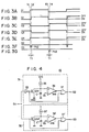
- Figs. 3A through 3G show a set of waveforms useful in explaining the operation mode of each transistor in the circuit of Fig. 2.
- Fig. 3A shows a waveform of a signal S1 at the input terminal 10B.
- Figs. 3B through 3E show waveforms of the collector voltages of the transistors Ql-Q4. In the figures, the high level indicates an off state, and the low level, an on state.
- Figs. 3F and 3G show waveforms of the output signals from pulse generator 15.
- the output signal from control circuit 11 causes transistor Q11 to turn on.
- transistors Q9 and Q5 constituting a current mirror circuit are also turned on.
- transistor Q1 is appropriately biased to be turned on.
- transistors Q8 and Q4 connected in a Darlington fashion are appropriately biased to turn on.
- current flows from the terminals M(+) to M(-) of motor 12, and motor 12 is rotated forwardly.
- the output signal from control circuit 11 causes transistors Q12, Q10 and Q6 to be turned on.
- Transistor Q2 is appropriately biased through transistor Q6, and also transistors Q7 and Q3 are biased through transistor Q10.
- resistors R1 to R6 are provided for preventing an erroneous operation of the circuit due to a leak current, and reduction of an off-time in the switching operation of the transistor, that is, reduction of the carrier storage effect.
- the state of transistors Q1 and Q4 is reversed from an on-state to an off-state, and the state of transistors Q2 and Q3 is reversed from the off-state to the on-state.
- Such a reverse of the transistors results from the control of transistors Q5, Q9, Q11, Q6, Q10 and Q12 by control circuit 11.
- Transistor Q1 requires a period T1 of time from time t1 until it is completely turned off (t2). This is due to the carrier storage effect of the transistor per se. During the period T1, transistors Q1 and Q3 are concurrently turned on in the case of the Fig. 1 circuit of the prior art.
- the output signal S2 from the pulse generator 15, as shown in Fig. 3F is applied to the base of transistor Q7.
- the output signal S2 contains a pulse PS2 to delay the turning on of transistor Q3, which otherwise is turned on at time t1, till time t2, that is to say, to delay the turning on operation by the period T1.
- transistor Q3 Upon receipt of the pulse PS2, transistor Q3 is not turned on until transistor Q1 is sufficiently in an off-state (at time t2). Therefore, it is prevented for transistors Q1 and Q3 to be concurrently turned on. This implies that no through-current flows through the series circuit of transistors Q1 and Q3.
- Transistor Q2 takes period T1 from time t3 till it is completely in the off-time (at time t4), due to the carrier storage effect of transistor Q2. During this period T1, in the prior circuit of Fig. 1, transistors Q2 and Q4 are concurrently turned on.
- pulse generator 15 applies an output signal S3 as shown in Fig. 3G to the base of transistor Q8.
- the output signal S3 contains pulse PS3 to delay the turning on of transistor Q4, which otherwise turns on at time t3, till time t4, that is, to delay it by period T1.
- transistor Q3, upon receipt of the pulse PS3, is not turned on until transistor Q3 is sufficiently in the off-state (at time t4). Therefore, transistors Q2 and Q4 are never turned on concurrently. Further, no through current flows into the series circuit of transistors Q3 and Q4.
- Fig. 4 is a schematic circuit diagram showing an arrangement of the pulse generator 15 in the current flow reversing circuit shown in Fig. 2.
- reference numeral 31 generally designates as a first pulse generating circuit which receives an input signal S1 and produces a first signal S2.
- a second generating circuit S2 receives the same input signal S1 and produces a second signal S3.
- reference numeral 33 designates an inverter which reverses the phase of the input signal S1.
- An NPN transistor Q34 serving as an input switch, is connected at the base to the output signal from the above inverter 33 and grounded at the emitter, and connected at the collector through a constant current source 35 (or a resistor) to the power source V cc .
- C is a capacitor connected between the collector of the transistor Q34 and ground.
- Numeral 36 stands for a voltage comparator which is connected at the noninverting (+) input terminal to the collector of the transistor Q34 and at the inverting input terminal (-) to a reference voltage Vs (a predetermined voltage between the .power voltage V cc and the ground potential).
- An OR circuit 37 ORs the outputs of the comparator 36 and the inverter 33, to produce a signal S2.
- the second pulse generating circuit 32 is different from the first pulse generating circuit 31 only in the following points.
- the inverter 33 is omitted, the input signal S1 is directly led to the transistor Q34 as the input switch and to the OR circuit 37, not through the inverter. Therefore, in the second pulse generator, primed reference numerals are used for designating like portions in the first pulse generator.
- Fig. 5 shows a higher schematic diagram of the pulse generator shown in Fig. 4.
- the voltage comparator 36 includes PNP transistors Q41 and Q42 for differential operation, which are connected together at the emitters, a resistor R43 connected between the emitter interconnection point and the power source V cc , NPN transistors Q44 and Q46 which are connected in a current mirror fashion and respectively serve as loads of the transistors Q41 and Q42, drive transistors Q46 and Q47 for driving the bases of the differential transistors Q41 and Q42, and resistors R48 and R49 respectively serving as the loads of the drive transistors Q46 and Q47.
- the OR circuit 37 includes two NPN transistors Q50 and Q51 which are respectively connected at the bases to two output signals (a collector voltage of a transistor Q45 and a base voltage of a transistor Q34), and grounded at the emitters, and interconnected at the collector, a load resistor R52 which is connected between the above collector interconnecting point and the power source V cc , an NPN transistor Q53 of which the collector serves as an output terminal for the signal S2, and which is connected at the base to the collector interconnecting point, and grounded at the emitter.
- the inverter 33 includes an PNP transistor Q54 which is connected at the base to the input signal S1, and grounded at the emitter, and connected at the collector to the power source V cc through a load resistor R55.
- the bases of the transistor Q34 and Q51 are connected to current restricting resistors R56 and R57, respectively.
- the resistors R43, R48, R49, R52 and R55 may be substituted by constant current source circuits, respectively.
- the circuit arrangement of the pulse generating circuit 32 is the same as that of the pulse generating. circuit 31.
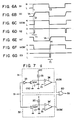
- the operation of the pulse generator 15 of the Fig. 4 will be described, referring to time charts shown in Figs. 6A to 6G.
- the input signal S1 (Fig. 6A) is L in level (in this case, a forward mode is set up)
- the output from the inverter 33 is H in level
- the transistor Q34 is in an on-state. Therefore, the input voltage (the voltage across the capacitor C) to the comparator 36 is at ground potential (Fig. 6B).
- the output voltage Vo36 of the comparator is L (Fig. 6C).
- This L level signal and the output signal of the inverter 32 are applied to the inputs of the OR circuit 37, respectively.
- the OR circuit 37 produces an H level signal (Fig. 6D).
- the transistor Q34' is in the off-state since the input signal S1 is in L level.
- the input signal to the comparator 36' is higher than the reference input voltage Vs.
- the input signal is the voltage Vc' across the capacitor C' which is equal to the power voltage V cc since the capacitor is fully charged.
- the output signal Vo36' of the comparator is in H level (Fig. 6F).
- the output signal S3 from the OR circuit 37' is in H level.
- the first pulse generating circuit 31 operates such that the output signal of the inverter 33 is L in level and the transistor Q34 is in an off-state. Under this condition, a constant current 135 derived from the constant current source 35 starts the charge of the capacitor C. At this time, both input signals to the OR circuit 37 are L, so that the output signal S2 is inverted in level to be L. After a fixed period of time T1 (time t2), the voltage Vc across the capacitor C (Fig.
- the fixed period T1 corresponds to the pulse width of the output signal (the L level duration of the output signal S2), and is given where C is capacitance of the capacitor C.
- the second pulse generator circuit 32 operates such that the transistor Q34' is in an on-state, the capacitor C' is discharged, and the output signal Vo36' of the capacitor 36' becomes L in level (Fig. 6F).
- one (i.e. the input signal S1) of the input signals to the OR circuit 37' is in H level.
- the output signal S3 remains H in level (Fig. 6G).
- the output signal Vo36 of the comparator 36 of the first pulse generating circuit 31 is in H level.
- the output signal S3 of the OR circuit 37 is kept H in level.
- one (input signal S1) of the input signals to the OR circuit 37' is H, and the output signal S3 remains H in level.
- the input signal S1 changes its signal state from H level to L level (the forward mode is selected).
- the inverter 33 ' produces an H level signal, and the transistor is in an on-state.
- the output signal of the comparator 36 becomes L in level.
- one (the output signal of the inverter 33) of the input signals to the OR circuit 37 is H in level.
- the Output signal S2 is still in H level.
- the transistor Q34' is in an off-state, and charging to the capacitor C'starts.
- the inputs of the OR circuit 37' are both in L level.
- the output signal S3 becomes H in level.
- the output signal of the comparator 36' is level inverted to be H in level.
- the output signal S3 of the OR circuit 37' returns its level to H.
- the pulse generator 15 produces the signals S2 and S3 shown in Figs. 3F and 3G (Figs. 6D and 6G) through a sequence of operations as described above referring to Figs. 6A to 6G.
- the signals S2 and S3 may be replaced by the output signals Vo36 and Vo36' of the comparators 36 and 36' in the first and second pulse generating circuits 31 and 31', respectively.
- Fig. 7 shows a schematic diagram of another arrangement of the pulse generator 15.
- the circuit arrangement of this embodiment is the same as that of Fig. 4, except the wiring to the OR circuit.
- a single OR circuit ORs the output signal Vo36 of the first pulse generating circuit 31 and the output signal Vo36' of the second pulse generating circuit 32 to produce a signal So as the logical sum of the signals S2 and S3.
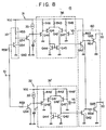
- the details of the circuit arrangement of Fig. 7 is as illustrated in Fig. 8.
- the OR circuit 60 is comprised of two input NPN transistors Q61 and Q62, a load resistor R63, and two output circuits for providing two paths to the ORed output signal (of the signals S2 and S3).
- One of the output circuits includes a resistor R64 and an output NPN transistor Q65.
- the other includes a resistor R64' and an NPN output transistor Q65'.
- the base of the transistor Q61 is connected to the collector of the transistor Q45.
- the transistor Q61 is connected at the emitter to ground and at the collector to the load resistor R63 and further to one end of the resistor R64 and the collector of the transistor Q62.
- the base of the transistor Q65 is connected to the other end of the resistor R64.
- the emitter of the same is grounded. Further, the collector of this transistor serves as an output terminal for the signal So.
- the other output circuit has a similar connection to the above one.
- the pulse generator 15 thus arranged will operate according to timing charts shown in Figs.
- the waveforms of Figs. 9A to 9F correspond to those of Figs. 6A-6C; the waveforms of Figs. 9D and 9E, to those of Figs. 6E and 6F; and the waveform of Fig. 9F is the compposite waveform of those of Figs. 6D and 6G.
- the OR circuit of Fig. 8 has two outputs, while that of Fig. 7 has one output.
- the reason for this is that the OR circuit of Fig. 7 is depicted in the logic form, but that of Fig. 8 is depicted as an converter circuit.
- Fig. 10 shows a basic circuit diagram of a further arrangement of the pulse generator 15.
- An NPN transistor Q71 is an input transistor and an NPN transistor Q72 is an output transistor.
- the base of the input transistor Q71 is applied with the input signal S1 (fig. 11A).
- the collector of the transistor Q71 is connected to the V cc potential V cc through an electric current source 73.
- the emitter of the transistor Q71 is connected to ground through a capacitor C.
- the collector of the transistor Q72 is connected to the V cc higher potential through an electric current source 74.
- the output signal So is obtained at the collector of the transistor Q72.
- the base of the transistor Q72 is connected to ground through the capacitor C.
- the emitter of the transistor Q72 is connected to ground.
- 1 1 and 1 2 are selected to have the following unequality (3). where, 1 1 is an electric current which the current source 73 supplies and 1 2 is an electric current which the current source 74 supplies.
- AV is obtained as about 60 (mV) from the following equation (7).
- Fig. 12 shows a detailed circuit diagram of the pulse generator constituted based on the basic circuit of Fig. 10. All transistors Q81 to Q92 are of NPN type. Transistors Q86 and Q87 constitutes a differential circuit. The collectors of the transistors Q86 and Q87 are connected to the power source potential V cc through a resistor R95. The emitters of the transistors Q86 and Q87 are connected to ground. Input signal S1 is applied to the gate of the transistor Q81. The collector of the transistor Q81 is connected to the power source potential V cc through a resistor R91. The emitter of the transistor Q81 is connected to ground. The collector of the transistor Q81 is also connected to the gate of the transistor Q82 through a resistor R82.
- the collector of the transistor Q82 is connected to the power source potential V cc through a resistor R92.
- the emitter of the transistor Q82 is connected to ground.
- the collector of the transistor Q82 is also connected to the gate of the transistor Q83.
- the collector of the transistor Q83 is connected to the power source potential V cc through a resistor R93.
- the emitter of the transistor Q83 is connected to the collector of the transistor Q84 and the gate of the transistor Q85.
- the emitter of the transistor Q84 is connected to ground.
- the collector of the transistor Q85 is connected to the power source potential V cc through a resistor R94.
- the emitter of the transistor Q85 is connected to the gate of the transistor Q84 and ground.
- the collector of the transistor Q85 is also connected to the gate of the transistor Q86.
- the gate of the transistor Q87 is connected to the collector of the transistor Q88.
- the collector of the transistor Q88 is connected to the power source potential V cc through a resistor R96.
- the emitter of the transistor Q88 is connected to the gate of the transistor Q89 and ground.
- the collector of the transistor Q89 is connected to the emitter of the transistor Q90 and the gate of the transistor Q88.
- the emitter of the transistor Q89 is connected to ground.
- the collector of the transistor Q90 is connected to the power source potential V cc through a resistor R97.
- the emitter of the transistor Q89 is connected to the collector of the transistor Q81.
- the collectors of the transistors Q86 and Q87 are also connected to the gate of the transistor Q91 through a resistor R83.
- the collectors of the transistors Q86 and Q87 are further connected to the gate of the transistor Q92 through a resistor R84.
- the emitters of the transistors Q91 and Q92 are connected to ground.
- Output signals S2 and S3 are obtained at the collector of the transistor Q91 and the collector of the transistor Q92, respectively.
- the capacitance C in the basic circuit of Fig. 10 may be formed by the capacitance Ccs between the collector of the transistor Q84 and substrate and the capacitance Ccs between the collector of the transistor Q89 and substrate, or the capacitance Ccb between the collector and base of the transistor Q84 and the capacitance Ccb between the collector and the base of the transistor Q89.
- Figs. 13A to 13G show time charts of signals of various portions of the Fig. 12 circuit.
- Figs. 13A and 13B show input and output signals, respectively.
- Figs. 12B, 12C, 12D, 12E and 12F show the signals of the collectors of the transistors Q81, Q82, Q85, Q88 and Q86, respectively.
- Fig. 14 shows a schematic circuit diagram of the control circuit 11 in the reversing circuit of Fig. 2.
- the control circuit 11 comprises two NAND gates 101 and 102 and an inverter 103.
- One input terminal of NAND gate 101 is connected to the input terminal 10A and one input terminal of NAND gate 102 is also connected to the input terminal10A.
- the other input terminal of NAND gate 101 is connected to the inputterminal 10B through the inverter 103.
- the other input terminal of NAND gate 102 is directly connected to the input terminal 10B.
- the output terminal of NAND gate 101 is connected to the collector of the transistor Q11.
- the output terminal of NAND gate 102 is connected to the collector of the transistor Q12.
- the present invention is additionally provided with a means for applying a pulse to delay the timing at which transistors Q3 and Q4 are reversed from the on-state to the off-state.
- the provision of the timing delaying means compensates for the delay mf the reverse from the on-state to the off-state of transistors Q1 and Q2, which is due to the carrier storage effect, and therefore, prevents the flow of the through current.
- the timing delaying means compensates for the delay mf the reverse from the on-state to the off-state of transistors Q1 and Q2, which is due to the carrier storage effect, and therefore, prevents the flow of the through current.
- the reliability of the currentflow reverse circuit is improved, together with the design freedom of the peripheral circuit.
- the present invention is applied to the current flow reverse circuit for reversing an electrical current flow to the DC motor, it is of course applicable for various types of load circuits in which the flow direction of the current flowing through the load must be reversed.
Landscapes
- Engineering & Computer Science (AREA)
- Power Engineering (AREA)
- Control Of Direct Current Motors (AREA)
Description
- The present invention relates to a current flow reversing circuit, and more particularly, to a current flow reversing circuit for reversing the flow of current to a motor.
- A typical example of the circuit for reversing the flow of current flowing into a DC motor is shown in Fig. 1. As shown, an output signal from a control circuit as a logical circuit is used for setting up a stop mode, a forward mode and a reverse mode of a
motor 12. Relationships among logic levels of control signals applied to the terminals M(+) and M(-) ofmotor 12 and theinput terminals control circuit 11, and the respective modes are tabulated as below.
- In the above table, H denotes a high level and L denotes a low level. In a forward mode, the output signal of the
control circuit 11 turns on a transistor Q11, and also transistors Q9 and Q5. These transistors Q11, Q9 and Q5 form a current mirror circuit. Upon turning on transistor Q5, a transistor Q1 is appropriately biased to turn on. When transistor Q9 is turned on, transistors Q8 and Q4, which are connected in a Darlington fashion, are appropriately biased and turned on. Then, current flows from the terminal M(+) to the terminal M(-) ofmotor 12,motor 12 is rotated in the forward direction. For turning the motor in the reverse direction, the output signal ofcontrol circuit 11 turns on transistors Q12, Q10 and Q6. Subsequently, transistor Q2 is appropriately biased by transistor Q6. Transistors Q7 and Q3 are also biased by transistor Q10 and turned on. Consequently, the current flows from the terminal M(-) to the terminal M(+), andmotor 12 rotates in the reverse direction. For stopping the motor, transistors Q11 and Q12 are both turned off. Accordingly, transistors Q1 to Q4 are not biased and no current is fed tomotor 12, thereby to stopmotor 12. - In the above circuit,.resistors R1 to R6 are provided for preventing an erroneous operation of the circuit due to a leak current, and for reducing the off-time of the switching operation of the transistor, viz. reducing the carrier storage effect. The off-time means a time interval between an on-state of the transistor and an off-state.
- The terminal currents IOLf and lOLr of
motor 12 in the forward and the reverse modes are mathematically expressed by

- RL: Resistance of the motor.
- Vcc: Voltage on
power line 13. - VBEQ1: Voltage across the base-emitter path of transistor Q1.
- VCE(sat)Q5: Voltage across the collector-emitter path of transistor Q5.
- VBEQ4: Voltage across the base-emitter path of transistor Q4.
- VCE(sat)· Voltage across of the collector-emitter path of saturated transistor Q8.
- In order to increase the currents lOLf and lOLr to the amplitude enough to drive
motor 12, a sufficient base current is fed to each transistor Q1 to Q4. - In the above circuit, when
motor 12 is steady in the forward or the reverse mode, the current as given by the equation (1) or (2), flows throughmotor 12. However, if a time period taken for transistor Q1 or Q2 to change in its state from the. on-state to the off-state, viz. a called off-time, is long, a through current flows- through a series circuit comprising transistors Q1 and Q3 or that of transistors Q2 and Q4. - Let us consider a case where a circuit state, in which transistors Q2 and Q3 are in the on-state and transistors Q1 and Q4 are in the off-state (reverse mode), is switched to another state in which transistors Q1 and Q4 are in the on-state and transistors Q2 and Q3 are in the off-state. In this case, if the switching of the transistor to the off-state is delayed, that is, the off-time is long, a through-current flows into the series circuit of transistors Q2 and Q4. The electric current frequently damages transistors Q2 and Q4 or their peripheral circuits.
- The switching delay causing the through current is due to the carrier storage effect of the element when its state is switched from the on-state to the off-state. In the case of the transistors Q1 and Q4, the carrier storage effect changes dependent on the operating current ICQ5 and ICQ9 flowing through transistors Q5 and Q9, which bias transistors Q1 and Q4. The operation current ICQ5 and ICQ9 are given by


- As seen from the equation (5), current flowing into transistor Q5 is hFEQ8 times the current flowing into transistor Q9. This implies that the area of transistor Q5 must be much larger than that of transistor Q9, which in turn implies that the storage effect of transistor Q1 is increased accordingly.
- Prior art document JP-A-15 43 78 discloses a control circuit for a motor. In this control circuit, when a start control signal is set to "H" level, the output of an AND circuit becomes "H" level, and when a rotating direction instruction signal is set to "H" level, first and second control transistor Qi, Q2 become ON, and a motor rotates normally. When the instruction signal is set to "L" level, first and third transistors becomes OFF, while second transistors becomes ON. Then, the output of the AND circuit becomes "H" level in delay by the time corresponding to the time constant of the delay circuit having a resistor and a condenser, the third transistor becomes ON, and the motor rotates reversely. In this manner, the shortcircuit of the control transistors can be prevented.
- An object of the present invention is to provide a circuit for reversing the flow of electric current to an apparatus, such as a DC motor, which prevents a through current from flowing into the apparatus.
- The present invention provides a current flow reversing circuit as defined in claim 1.
- This invention can be more fully understood from the following detailed description when taken in conjunction with the accompanying drawings, in which:
- Fig. 1 is a diagram of a prior circuit for reversing the flow of electric current fed to a DC motor;
- Fig. 2 is a diagram of a circuit for reversing the flow of electric current according to an embodiment of the invention applied to a DC motor;
- Figs. 3A through 3G show time charts of signals at various portions in the circuit of Fig. 2;
- Fig. 4 shows a schematic diagram of the pulse generator of the current flow reversing circuit of Fig. 2;
- Fig. 5 is a circuit diagram of the pulse generator of Fig. 4;
- Figs. 6A-6G show timing charts illustrating the operation of the pulse generator of Fig. 4;
- Fig. 7 shows a schematic diagram of another pulse generator;
- Fig. 8 shows a circuit diagram of the pulse generator of Fig. 7;
- Figs. 9A-9F show timing charts illustrating the operation of the pulse generator of Fig. 7;
- Fig. 10 shows a basic circuit diagram of another arrangement of the pulse generator;
- Figs. 11A and 11B show timing charts of input and output signals of the pulse generator of Fig. 10, respectively;
- Fig. 12 shows a detailed circuit diagram of the pulse generator constituted by the basic circuit of Fig. 10;
- Figs. 13A to 13G show timing charts of various portions of the pulse generator of Fig. 12; and
- Fig. 14 shows a circuit diagram of the control circuit in the reversing circuit of Fig. 2.
- Turning now to Fig. 2, there is shown a circuit for reversing the flow of current fed to a DC motor, which is an embodiment of the present invention. As shown, a
pulse generator circuit 15 is additionally used in the prior circuit shown in Fig. 1. Thecircuit 15 contains, for example, a differential circuit and a waveshaping circuit, and receives a signal S1 from aninput terminal 10B, and produces first and second output signals S2 and S3. - In Fig. 2, a
control circuit 11 comprises a logic circuit for controlling the operation modes of amotor 12.Control circuit 11 has twoinput terminals Logic circuit 11 also has two output terminals. The positive polarity terminal M(+) ofmotor 12 is connected through NPN transistor Q1 topower source line 13.Power source line 13 is connected to a power source of a high potential Vcc. The collector of transistor Q1 is connected topower source line 13. The emitter of transistor Q1 is connected to positive terminal M(+) ofmotor 12. The base and emitter of transistor Q1 are interconnected through a resistor R1. - The positive polarity terminal M(+) of
motor 12 is connected through NPN transistor Q1 topower source line 13.Power line 13 is connected to a power source of a high potential Vcc. The collector of transistor Q1 is connected topower source line 13. The emitter of transistor Q1 is connected to positive terminal M(+) ofmotor 12. The base and emitter of transistor Q1 are interconnected through a resistor R1. The positive terminal M(+) ofmotor 12 is. also connected through NPN transistor Q3 to ground GND. The collector of transistor Q3 is connected to positive terminal M(+) ofmotor 12. The emitter of transistor Q3 is connected to ground GND. The negative polarity terminal M(-) ofmotor 12 is connected through NPN transistor Q2 topower source line 13. The collector of transistor Q3 is connected topower source line 13. The emitter of transistor Q2 is connected to the positive terminal M(+) ofmotor 12. The base and emitter of transistor Q2 are interconnected through a resistor R2. The negative terminal M(-) ofmotor 12 is also connected through NPN transistor Q4 to ground GND. The collector of transistor Q4 is connected to the negative terminal M(-) ofmotor 12. The emitter of transistor Q4 is connected to ground GND. - Resistors R1 and R5, and PNP transistor Q5, Q9 and Q11 constitute a bias circuit for transistor Q1. NPN transistor Q11 constitutes a current mirror circuit together with PNP transistors Q9 and Q5. The emitters of transistors Q11, Q9 and Q5 are connected to the
power source line 12. The bases of transistors Q11, Q9 and Q5 are interconnected. The bases of transistors Q11 and Q9 are connected to powersource line 13 through a resistor R5. The collector of transistor Q11 is connected to one of the output terminals ofcontrol circuit 11. The base and collector of transistor Q11 are interconnected. The collector of transistor Q9 is connected to the base of transistor Q8. The collector of transistor Q5 is connected to the base of transistor Q1. - Resistors R2 and R6, and PNP transistors Q6, Q10 and Q12 constitute a bias circuit for transistor Q2. PNP transistor Q12 constitutes a current mirror circuit together with PNP transistors Q10 and Q6. The emitters of transistors Q12, Q10 and Q6 are connected to power
source line 13. The bases of transistors Q12, Q10 and Q6 are interconnected. The bases of transistors Q12 and Q10 are connected to powersource line 13 through a resistor R6. The collector of transistor Q12 is connected to the other output terminal ofcontrol circuit 11. The base and collector of transistor Q12 are interconnected. The collector of transistor Q10 is connected to the base of transistor Q7. The collector of transistor Q6 is connected to the base of transistor Q2. - An NPN transistor Q7 constitutes a bias element for transistor Q3. The collector-emitter path of transistor Q7 is connected across the collector and base of transistor Q3. The collector of transistor Q7 is connected to the collector of transistor Q3. The transistor Q7 is also connected to ground GND through a resistor R3. The base of transistor Q7 is connected to the collector of transistor Q10.
- An NPN transistor Q8 constitutes a bias element for transistor Q8. The collector-emitter path of transistor Q8 is connected across the collector and base of transistor Q4. The collector of transistor Q8 is connected to the collector of transistor Q4. The emitter of transistor Q8 is connected to the base of transistor Q4. The emitter of transistor Q8 is also connected to ground GND through a resistor R4. The base of transistor Q8 is connected to the collector of transistor Q9.
-
Pulse generator 15 has an input terminal and two output terminals. The input terminal ofpulse generator 15 is connected to theinput terminal 10B ofcontrol circuit 11. One of the output terminals ofpulse generator 15, at which an output signal S2 appears, is connected to the base of transistor Q7 and the collector of transistor Q10. The other output terminal ofpulse generator 15, at which an output signal S3 appears, is connected to the base of transistor Q8 and the collector of transistor Q9. - According to the Fig. 2 embodiment, one of the stop, forward and reverse modes can be set according to the output signal from the
control circuit 11. The relationships among the logic levels at the terminals M(+) and M(-) ofmotor 12, logic levels of the control signals applied to theinput terminals control circuit 11, and the respective modes are tabulated as below.
- Figs. 3A through 3G show a set of waveforms useful in explaining the operation mode of each transistor in the circuit of Fig. 2. Fig. 3A shows a waveform of a signal S1 at the
input terminal 10B. Figs. 3B through 3E show waveforms of the collector voltages of the transistors Ql-Q4. In the figures, the high level indicates an off state, and the low level, an on state. Figs. 3F and 3G show waveforms of the output signals frompulse generator 15. - In the forward mode, viz. when
motor 12 forwardly rotates, the output signal fromcontrol circuit 11 causes transistor Q11 to turn on. At this time, transistors Q9 and Q5 constituting a current mirror circuit are also turned on. Upon turning on transistor Q5, transistor Q1 is appropriately biased to be turned on. When transistor Q9 is turned on, transistors Q8 and Q4 connected in a Darlington fashion are appropriately biased to turn on. As a result, current flows from the terminals M(+) to M(-) ofmotor 12, andmotor 12 is rotated forwardly. In the reverse mode, the output signal fromcontrol circuit 11 causes transistors Q12, Q10 and Q6 to be turned on. Transistor Q2 is appropriately biased through transistor Q6, and also transistors Q7 and Q3 are biased through transistor Q10. Then, current flows from the terminals M(-) to M(+), andmotor 12 is rotated reversely. In the stop mode, both the transistors Q11 and Q12 are turned off. Therefore, no bias potential is applied to transistors Q1 through transistor Q4, so that drive current is fed tomotor 12. As aresult motor 12 is stopped. - In the circuit as mentioned above, resistors R1 to R6 are provided for preventing an erroneous operation of the circuit due to a leak current, and reduction of an off-time in the switching operation of the transistor, that is, reduction of the carrier storage effect.
- The terminal currents lOLf and lOLr of the motor in the forward mode and reverse mode are respectively given


- RL: Resistance of
motor 12. - Vcc: Voltage on
power source line 13. - VBEQ1: Voltage across the base-emitter path of transistor Q1.
- VCE(sat): Voltage across the collector-emitter of saturated transistor Q5.
- VBEQ41 Voltage across the base-emitter path of transistor Q4.
- VCE(sat)Q8: Voltage across the collector-emitter of saturated transistor Q8.
- In order for the currents IOLf and Imr, as given by the equations (1) and (2) respectively, to drive
motor 12, sufficient currents are fed to the bases of transistors Q1 to Q4. - At time t1, the state of transistors Q1 and Q4 is reversed from an on-state to an off-state, and the state of transistors Q2 and Q3 is reversed from the off-state to the on-state. Such a reverse of the transistors results from the control of transistors Q5, Q9, Q11, Q6, Q10 and Q12 by
control circuit 11. - Transistor Q1 requires a period T1 of time from time t1 until it is completely turned off (t2). This is due to the carrier storage effect of the transistor per se. During the period T1, transistors Q1 and Q3 are concurrently turned on in the case of the Fig. 1 circuit of the prior art. In the Fig. 2 circuit of the present embodiment, the output signal S2 from the
pulse generator 15, as shown in Fig. 3F, is applied to the base of transistor Q7. The output signal S2 contains a pulse PS2 to delay the turning on of transistor Q3, which otherwise is turned on at time t1, till time t2, that is to say, to delay the turning on operation by the period T1. Upon receipt of the pulse PS2, transistor Q3 is not turned on until transistor Q1 is sufficiently in an off-state (at time t2). Therefore, it is prevented for transistors Q1 and Q3 to be concurrently turned on. This implies that no through-current flows through the series circuit of transistors Q1 and Q3. - This is true for the control that the state of transistors Q2 and Q3 are reversed from the on-state to the off-state, and the state of transistors Q1 and Q4 are reversed from the off-state to the on-state. Transistor Q2 takes period T1 from time t3 till it is completely in the off-time (at time t4), due to the carrier storage effect of transistor Q2. During this period T1, in the prior circuit of Fig. 1, transistors Q2 and Q4 are concurrently turned on. On the other hand, in the present embodiment shown in Fig. 2,
pulse generator 15 applies an output signal S3 as shown in Fig. 3G to the base of transistor Q8. The output signal S3 contains pulse PS3 to delay the turning on of transistor Q4, which otherwise turns on at time t3, till time t4, that is, to delay it by period T1. Thus, transistor Q3, upon receipt of the pulse PS3, is not turned on until transistor Q3 is sufficiently in the off-state (at time t4). Therefore, transistors Q2 and Q4 are never turned on concurrently. Further, no through current flows into the series circuit of transistors Q3 and Q4. - Fig. 4 is a schematic circuit diagram showing an arrangement of the
pulse generator 15 in the current flow reversing circuit shown in Fig. 2. In the pulse generator shown in Fig. 4,reference numeral 31 generally designates as a first pulse generating circuit which receives an input signal S1 and produces a first signal S2. A second generating circuit S2 receives the same input signal S1 and produces a second signal S3. In the firstpulse generating circuit 31,reference numeral 33 designates an inverter which reverses the phase of the input signal S1. An NPN transistor Q34, serving as an input switch, is connected at the base to the output signal from theabove inverter 33 and grounded at the emitter, and connected at the collector through a constant current source 35 (or a resistor) to the power source Vcc. C is a capacitor connected between the collector of the transistor Q34 and ground.Numeral 36 stands for a voltage comparator which is connected at the noninverting (+) input terminal to the collector of the transistor Q34 and at the inverting input terminal (-) to a reference voltage Vs (a predetermined voltage between the .power voltage Vcc and the ground potential). An ORcircuit 37 ORs the outputs of thecomparator 36 and theinverter 33, to produce a signal S2. The secondpulse generating circuit 32 is different from the firstpulse generating circuit 31 only in the following points. Theinverter 33 is omitted, the input signal S1 is directly led to the transistor Q34 as the input switch and to theOR circuit 37, not through the inverter. Therefore, in the second pulse generator, primed reference numerals are used for designating like portions in the first pulse generator. - Fig. 5 shows a higher schematic diagram of the pulse generator shown in Fig. 4. In the
pulse generating circuit 31 in Fig. 4, thevoltage comparator 36 includes PNP transistors Q41 and Q42 for differential operation, which are connected together at the emitters, a resistor R43 connected between the emitter interconnection point and the power source Vcc, NPN transistors Q44 and Q46 which are connected in a current mirror fashion and respectively serve as loads of the transistors Q41 and Q42, drive transistors Q46 and Q47 for driving the bases of the differential transistors Q41 and Q42, and resistors R48 and R49 respectively serving as the loads of the drive transistors Q46 and Q47. The ORcircuit 37 includes two NPN transistors Q50 and Q51 which are respectively connected at the bases to two output signals (a collector voltage of a transistor Q45 and a base voltage of a transistor Q34), and grounded at the emitters, and interconnected at the collector, a load resistor R52 which is connected between the above collector interconnecting point and the power source Vcc, an NPN transistor Q53 of which the collector serves as an output terminal for the signal S2, and which is connected at the base to the collector interconnecting point, and grounded at the emitter. Theinverter 33 includes an PNP transistor Q54 which is connected at the base to the input signal S1, and grounded at the emitter, and connected at the collector to the power source Vcc through a load resistor R55. The bases of the transistor Q34 and Q51 are connected to current restricting resistors R56 and R57, respectively. The resistors R43, R48, R49, R52 and R55 may be substituted by constant current source circuits, respectively. In Fig. 4, the circuit arrangement of thepulse generating circuit 32 is the same as that of the pulse generating.circuit 31. - The operation of the
pulse generator 15 of the Fig. 4 will be described, referring to time charts shown in Figs. 6A to 6G. When the input signal S1 (Fig. 6A) is L in level (in this case, a forward mode is set up), in the firstpulse generating circuit 31, the output from theinverter 33 is H in level, and the transistor Q34 is in an on-state. Therefore, the input voltage (the voltage across the capacitor C) to thecomparator 36 is at ground potential (Fig. 6B). The output voltage Vo36 of the comparator is L (Fig. 6C). This L level signal and the output signal of theinverter 32 are applied to the inputs of theOR circuit 37, respectively. The ORcircuit 37 produces an H level signal (Fig. 6D). In the secondpulse signal generator 32, the transistor Q34' is in the off-state since the input signal S1 is in L level. The input signal to the comparator 36' is higher than the reference input voltage Vs. The input signal is the voltage Vc' across the capacitor C' which is equal to the power voltage Vcc since the capacitor is fully charged. Then, the output signal Vo36' of the comparator is in H level (Fig. 6F). The output signal S3 from the OR circuit 37' is in H level. - Under this condition, when, at time t1, the input signal S1 changes its level from L level to H level (i.e. the reverse mode is selected), the first
pulse generating circuit 31 operates such that the output signal of theinverter 33 is L in level and the transistor Q34 is in an off-state. Under this condition, a constant current 135 derived from the constantcurrent source 35 starts the charge of the capacitor C. At this time, both input signals to theOR circuit 37 are L, so that the output signal S2 is inverted in level to be L. After a fixed period of time T1 (time t2), the voltage Vc across the capacitor C (Fig. 6B) exceeds the reference voltage Vs, the output signal Vo36 of thecomparator 36 is H, and then the output signal S2 of theOR circuit 37 is returned to be H in level. In this case, the fixed period T1 corresponds to the pulse width of the output signal (the L level duration of the output signal S2), and is given
- When the constant
current source 35 is substituted by the resistor R, the period T1 is given
- At time t1, the second
pulse generator circuit 32 operates such that the transistor Q34' is in an on-state, the capacitor C' is discharged, and the output signal Vo36' of the capacitor 36' becomes L in level (Fig. 6F). At this time, one (i.e. the input signal S1) of the input signals to the OR circuit 37' is in H level. The output signal S3 remains H in level (Fig. 6G). Subsequently, when the input signal S1 is in H level or the reverse mode is selected, the output signal Vo36 of thecomparator 36 of the firstpulse generating circuit 31 is in H level. The output signal S3 of theOR circuit 37 is kept H in level. In the secondpulse generating circuit 32, one (input signal S1) of the input signals to the OR circuit 37' is H, and the output signal S3 remains H in level. - At time t3, the input signal S1 changes its signal state from H level to L level (the forward mode is selected). In the first
pulse generating circuit 31, theinverter 33' produces an H level signal, and the transistor is in an on-state. The output signal of thecomparator 36 becomes L in level. At this time, one (the output signal of the inverter 33) of the input signals to theOR circuit 37 is H in level. Under this circuit condition, the Output signal S2 is still in H level. On the other hand, in the secondpulse generating circuit 32, the transistor Q34' is in an off-state, and charging to the capacitor C'starts. At this time, the inputs of the OR circuit 37' are both in L level. The output signal S3 becomes H in level. At time t4 after the period T1 from time t3, the output signal of the comparator 36' is level inverted to be H in level. The output signal S3 of the OR circuit 37' returns its level to H. - The
pulse generator 15 produces the signals S2 and S3 shown in Figs. 3F and 3G (Figs. 6D and 6G) through a sequence of operations as described above referring to Figs. 6A to 6G. Alternatively, to prevent the through-current in the current flow reversing circuit of Fig. 2, the signals S2 and S3 may be replaced by the output signals Vo36 and Vo36' of thecomparators 36 and 36' in the first and secondpulse generating circuits 31 and 31', respectively. - Fig. 7 shows a schematic diagram of another arrangement of the
pulse generator 15. The circuit arrangement of this embodiment is the same as that of Fig. 4, except the wiring to the OR circuit. As shown, a single OR circuit ORs the output signal Vo36 of the firstpulse generating circuit 31 and the output signal Vo36' of the secondpulse generating circuit 32 to produce a signal So as the logical sum of the signals S2 and S3. The details of the circuit arrangement of Fig. 7 is as illustrated in Fig. 8. As shown, theOR circuit 60 is comprised of two input NPN transistors Q61 and Q62, a load resistor R63, and two output circuits for providing two paths to the ORed output signal (of the signals S2 and S3). One of the output circuits includes a resistor R64 and an output NPN transistor Q65. Similarly, the other includes a resistor R64' and an NPN output transistor Q65'. As shown, the base of the transistor Q61 is connected to the collector of the transistor Q45. The transistor Q61 is connected at the emitter to ground and at the collector to the load resistor R63 and further to one end of the resistor R64 and the collector of the transistor Q62. The base of the transistor Q65 is connected to the other end of the resistor R64. The emitter of the same is grounded. Further, the collector of this transistor serves as an output terminal for the signal So. The other output circuit has a similar connection to the above one. Thepulse generator 15 thus arranged will operate according to timing charts shown in Figs. 9A to 9F. Of the waveforms, the waveforms of Figs. 9A to 9C correspond to those of Figs. 6A-6C; the waveforms of Figs. 9D and 9E, to those of Figs. 6E and 6F; and the waveform of Fig. 9F is the compposite waveform of those of Figs. 6D and 6G. - The OR circuit of Fig. 8 has two outputs, while that of Fig. 7 has one output. The reason for this is that the OR circuit of Fig. 7 is depicted in the logic form, but that of Fig. 8 is depicted as an converter circuit.
- Applying the composite signal So (Fig. 9F) of the output signals S2 and S3 to the transistors Q3 and Q4, not only delays the switching operation of the transistor Q3 from the on-state to the off-state, but also causes the transistor Q4 to rapidly switch the turn-on to the turn-on. Therefore, even with presence of some delay in the switching operation of the transistor Q4 from the on-state to the off-state, the through-current passing through the series route of the transistors Q2 and Q4 can be prevented. Similarly, the switching operation of the transistor Q4 from the turn-on to the turn-on is delayed, and the transistor Q3 is rapidly switched from the on-state to the off-state. Therefore, if there is a delay in the switching operation of the transistor Q3 from the on-state to the off-state, the through-current passing through the route of the transistors Q.1 and Q3 can be prevented.
- Fig. 10 shows a basic circuit diagram of a further arrangement of the
pulse generator 15. - An NPN transistor Q71 is an input transistor and an NPN transistor Q72 is an output transistor. The base of the input transistor Q71 is applied with the input signal S1 (fig. 11A). The collector of the transistor Q71 is connected to the Vcc potential Vcc through an electric
current source 73. The emitter of the transistor Q71 is connected to ground through a capacitor C. The collector of the transistor Q72 is connected to the Vcc higher potential through an electriccurrent source 74. The output signal So is obtained at the collector of the transistor Q72. The base of the transistor Q72 is connected to ground through the capacitor C. The emitter of the transistor Q72 is connected to ground. In the circuit of Fig. 10, 11 and 12 are selected to have the following unequality (3).
current source 73 supplies and 12 is an electric current which thecurrent source 74 supplies. - In the circuit of Fig. 10, when the input signal S1 is H level, the capacitor C is changed with the electric current 11 to turn the transistor Q72 on. Thus, the output signal So (Fig. 11 B) is set at L level. The delay time T is shown as follows.

- When the input signal S1 is changed H level to L level, charge stored in the capacitor C is discharged through the base and emitters of the transistor Q72 to turn the transistor Q72 off. Thus, the output signal So is changed L level to H level. The delay time TH is shown as follows.

- △V=VB1-VB2.
- IBQ2=l2/hFEQ2·
- VB1 is a voltage drop appearing across the base and emitter of the transistor Q71 when the electric current 11 follows. IBQ72 is a base current flowing through the base of the transistor Q72. hFEQ72 is a current amplification factor of the transistor Q72.
- Assume now that

- In this case, AV is obtained as about 60 (mV) from the following equation (7).

- Therefore,


- Fig. 12 shows a detailed circuit diagram of the pulse generator constituted based on the basic circuit of Fig. 10. All transistors Q81 to Q92 are of NPN type. Transistors Q86 and Q87 constitutes a differential circuit. The collectors of the transistors Q86 and Q87 are connected to the power source potential Vcc through a resistor R95. The emitters of the transistors Q86 and Q87 are connected to ground. Input signal S1 is applied to the gate of the transistor Q81. The collector of the transistor Q81 is connected to the power source potential Vcc through a resistor R91. The emitter of the transistor Q81 is connected to ground. The collector of the transistor Q81 is also connected to the gate of the transistor Q82 through a resistor R82. The collector of the transistor Q82 is connected to the power source potential Vcc through a resistor R92. The emitter of the transistor Q82 is connected to ground. The collector of the transistor Q82 is also connected to the gate of the transistor Q83. The collector of the transistor Q83 is connected to the power source potential Vcc through a resistor R93. The emitter of the transistor Q83 is connected to the collector of the transistor Q84 and the gate of the transistor Q85. The emitter of the transistor Q84 is connected to ground. The collector of the transistor Q85 is connected to the power source potential Vcc through a resistor R94. The emitter of the transistor Q85 is connected to the gate of the transistor Q84 and ground. The collector of the transistor Q85 is also connected to the gate of the transistor Q86. The gate of the transistor Q87 is connected to the collector of the transistor Q88. The collector of the transistor Q88 is connected to the power source potential Vcc through a resistor R96. The emitter of the transistor Q88 is connected to the gate of the transistor Q89 and ground. The collector of the transistor Q89 is connected to the emitter of the transistor Q90 and the gate of the transistor Q88. The emitter of the transistor Q89 is connected to ground. The collector of the transistor Q90 is connected to the power source potential Vcc through a resistor R97. The emitter of the transistor Q89 is connected to the collector of the transistor Q81. The collectors of the transistors Q86 and Q87 are also connected to the gate of the transistor Q91 through a resistor R83. The collectors of the transistors Q86 and Q87 are further connected to the gate of the transistor Q92 through a resistor R84. The emitters of the transistors Q91 and Q92 are connected to ground. Output signals S2 and S3 are obtained at the collector of the transistor Q91 and the collector of the transistor Q92, respectively.
- In the Fig. 12 circuit, the capacitance C in the basic circuit of Fig. 10 may be formed by the capacitance Ccs between the collector of the transistor Q84 and substrate and the capacitance Ccs between the collector of the transistor Q89 and substrate, or the capacitance Ccb between the collector and base of the transistor Q84 and the capacitance Ccb between the collector and the base of the transistor Q89.
- Figs. 13A to 13G show time charts of signals of various portions of the Fig. 12 circuit. Figs. 13A and 13B show input and output signals, respectively. Figs. 12B, 12C, 12D, 12E and 12F show the signals of the collectors of the transistors Q81, Q82, Q85, Q88 and Q86, respectively.
- Fig. 14 shows a schematic circuit diagram of the
control circuit 11 in the reversing circuit of Fig. 2. Thecontrol circuit 11 comprises twoNAND gates inverter 103. One input terminal ofNAND gate 101 is connected to theinput terminal 10A and one input terminal ofNAND gate 102 is also connected to the input terminal10A. The other input terminal ofNAND gate 101 is connected to the inputterminal 10B through theinverter 103. The other input terminal ofNAND gate 102 is directly connected to theinput terminal 10B. The output terminal ofNAND gate 101 is connected to the collector of the transistor Q11. The output terminal ofNAND gate 102 is connected to the collector of the transistor Q12. - As seen from the foregoing description, the present invention is additionally provided with a means for applying a pulse to delay the timing at which transistors Q3 and Q4 are reversed from the on-state to the off-state. The provision of the timing delaying means compensates for the delay mf the reverse from the on-state to the off-state of transistors Q1 and Q2, which is due to the carrier storage effect, and therefore, prevents the flow of the through current. As a result, there is eliminated the damage of the transistors and the peripheral circuits by the through current. This fact implies that the reliability of the currentflow reverse circuit is improved, together with the design freedom of the peripheral circuit.
- While, in the above-mentioned embodiment, the present invention is applied to the current flow reverse circuit for reversing an electrical current flow to the DC motor, it is of course applicable for various types of load circuits in which the flow direction of the current flowing through the load must be reversed.
Claims (3)
Applications Claiming Priority (4)
| Application Number | Priority Date | Filing Date | Title |
|---|---|---|---|
| JP59093181A JPH0681528B2 (en) | 1984-05-10 | 1984-05-10 | Current switching control circuit |
| JP93181/84 | 1984-05-10 | ||
| JP276129/84 | 1984-12-28 | ||
| JP59276129A JPS61157277A (en) | 1984-12-28 | 1984-12-28 | Current switching control circuit |
Publications (3)
| Publication Number | Publication Date |
|---|---|
| EP0160896A2 EP0160896A2 (en) | 1985-11-13 |
| EP0160896A3 EP0160896A3 (en) | 1986-11-26 |
| EP0160896B1 true EP0160896B1 (en) | 1990-01-03 |
Family
ID=26434603
Family Applications (1)
| Application Number | Title | Priority Date | Filing Date |
|---|---|---|---|
| EP85105061A Expired - Lifetime EP0160896B1 (en) | 1984-05-10 | 1985-04-25 | Current flow reversing circuit |
Country Status (3)
| Country | Link |
|---|---|
| US (1) | US4651269A (en) |
| EP (1) | EP0160896B1 (en) |
| DE (1) | DE3575246D1 (en) |
Families Citing this family (20)
| Publication number | Priority date | Publication date | Assignee | Title |
|---|---|---|---|---|
| US4894598A (en) * | 1986-11-20 | 1990-01-16 | Staubli International Ag | Digital robot control having an improved pulse width modulator |
| JPH0833974B2 (en) * | 1987-08-19 | 1996-03-29 | ソニー株式会社 | Magnetic head drive circuit |
| JPH02285999A (en) * | 1989-04-26 | 1990-11-26 | Citizen Watch Co Ltd | Driving circuit for stepping motor |
| US4989127A (en) * | 1989-05-09 | 1991-01-29 | North American Philips Corporation | Driver for high voltage half-bridge circuits |
| JPH0770984B2 (en) * | 1990-07-10 | 1995-07-31 | 株式会社東芝 | LSI power supply circuit |
| JP2658549B2 (en) * | 1990-10-17 | 1997-09-30 | 日本電気株式会社 | Microcomputer |
| JP2716105B2 (en) * | 1991-06-24 | 1998-02-18 | 株式会社日立製作所 | Alternating constant current circuit |
| EP0527641B1 (en) * | 1991-08-12 | 1997-11-19 | Motorola, Inc. | H-bridge flyback recirculator |
| US5111381A (en) * | 1991-08-12 | 1992-05-05 | Motorola, Inc. | H-bridge flyback recirculator |
| DE4223208A1 (en) * | 1992-07-15 | 1994-01-20 | Papst Motoren Gmbh & Co Kg | Bridge circuit for operation of brushless DC motor - includes potential-shifting capacitor as source of auxiliary voltage for turn-on of each MOSFET connected to positive supply |
| DE4410211B4 (en) * | 1994-03-24 | 2005-07-21 | Atmel Germany Gmbh | Circuit arrangement for the switchable control of a load |
| DE19605834A1 (en) * | 1996-02-16 | 1997-08-21 | Siemens Ag | Method for driving a DC motor and device for carrying out this method |
| DE19631043A1 (en) * | 1996-08-01 | 1998-02-05 | Philips Patentverwaltung | Circuit arrangement for controlling a direct current motor which can be driven in two directions |
| DE19725835A1 (en) * | 1997-06-18 | 1999-01-21 | Siemens Ag | Integrated full-bridge circuit with four transistors |
| EP0895343B1 (en) * | 1997-07-28 | 2003-09-24 | STMicroelectronics S.r.l. | Sharing of external components for the control of the switching dead-time of a plurality of integrated devices cooperating in driving and R-L multiphase actuator |
| JP2001186771A (en) * | 1999-10-15 | 2001-07-06 | Seiko Epson Corp | Chopper circuit, chopper circuit control method, chopper-type charging circuit, electronic device, and timing device |
| US20030179022A1 (en) * | 2002-03-19 | 2003-09-25 | Robert Martin | Modulated current source difference mode emitter follower driver circuit |
| US7421193B2 (en) * | 2005-06-28 | 2008-09-02 | Kobayashi Herbert S | Digital motor control system and method |
| US8427084B2 (en) * | 2009-07-21 | 2013-04-23 | Herbert S. Kobayashi | Digital pulse width modulated motor control system and method |
| CN103580464B (en) * | 2013-10-13 | 2015-10-28 | 成都威特电喷有限责任公司 | Self-protection H bridge drive circuit |
Citations (1)
| Publication number | Priority date | Publication date | Assignee | Title |
|---|---|---|---|---|
| JPS58154378A (en) * | 1982-03-09 | 1983-09-13 | Japan Servo Co Ltd | Control circuit for motor |
Family Cites Families (7)
| Publication number | Priority date | Publication date | Assignee | Title |
|---|---|---|---|---|
| US3560829A (en) * | 1969-01-28 | 1971-02-02 | Gen Electric | Pulse width modulated bridge power amplifier with memory and lockout logic |
| US3579080A (en) * | 1969-11-13 | 1971-05-18 | Allis Louis Co | Zero deadband reversing control |
| SU729780A1 (en) * | 1975-02-24 | 1980-04-25 | Предприятие П/Я М-5237 | Reversible control rectifier |
| DE2558571C2 (en) * | 1975-12-24 | 1983-09-29 | Licentia Patent-Verwaltungs-Gmbh, 6000 Frankfurt | Arrangement for controlling a DC motor driving a switching mechanism |
| US4409527A (en) * | 1979-07-03 | 1983-10-11 | Sommeria Marcel R | Transistor motor control |
| GB2093287B (en) * | 1981-01-30 | 1984-04-04 | Tokyo Shibaura Electric Co | Motor drive apparatus |
| JPS57160370A (en) * | 1981-03-26 | 1982-10-02 | Fuji Electric Co Ltd | Feed circuit for load |
-
1985
- 1985-04-25 DE DE8585105061T patent/DE3575246D1/en not_active Expired - Lifetime
- 1985-04-25 EP EP85105061A patent/EP0160896B1/en not_active Expired - Lifetime
- 1985-05-02 US US06/729,662 patent/US4651269A/en not_active Expired - Lifetime
Patent Citations (1)
| Publication number | Priority date | Publication date | Assignee | Title |
|---|---|---|---|---|
| JPS58154378A (en) * | 1982-03-09 | 1983-09-13 | Japan Servo Co Ltd | Control circuit for motor |
Also Published As
| Publication number | Publication date |
|---|---|
| DE3575246D1 (en) | 1990-02-08 |
| EP0160896A3 (en) | 1986-11-26 |
| US4651269A (en) | 1987-03-17 |
| EP0160896A2 (en) | 1985-11-13 |
Similar Documents
| Publication | Publication Date | Title |
|---|---|---|
| EP0160896B1 (en) | Current flow reversing circuit | |
| JP3154665B2 (en) | High-side motor current detection circuit | |
| US8040162B2 (en) | Switch matrix drive circuit for a power element | |
| JP6261590B2 (en) | Circuits and related techniques for driving the high side of a half-bridge circuit | |
| EP0695679B1 (en) | Power steering apparatus for performing feedback control of motor-driving current | |
| US5663672A (en) | Transistor gate drive circuit providing dielectric isolation and protection | |
| JPH0145806B2 (en) | ||
| KR20040075024A (en) | Half-bridge driver and power conversion system with such driver | |
| JP7271933B2 (en) | Insulated gate device driver | |
| US4823056A (en) | Pulse-width modulation drive circuit | |
| EP0315597B1 (en) | Analog multiplex for sensing the magnitude and sense of the current through a h-bridge stage utilizing a single sensing resistance | |
| US7176693B2 (en) | Short circuit detecting circuit and abnormality monitoring signal generating circuit | |
| US5034875A (en) | Voltage multiplier circuit | |
| US5850129A (en) | Drive circuit for a three-phase brushless motor | |
| JP6642074B2 (en) | Driving device for switching element | |
| JPS59141131A (en) | Control circuit for bistable relay | |
| US8482232B2 (en) | Motor drive circuit | |
| JP2003338743A (en) | Power device drive circuit | |
| JP2688746B2 (en) | PWM drive circuit | |
| KR960009035Y1 (en) | Base driving control circuit of motor | |
| KR0112073Y1 (en) | Open collector driving circuit | |
| JP2798591B2 (en) | Magnetic head disconnection detection circuit | |
| JPH09190698A (en) | Sample hold circuit | |
| JPH02285971A (en) | Gate drive circuit for inverter | |
| JPH10262389A (en) | Drive device for brushless motor |
Legal Events
| Date | Code | Title | Description |
|---|---|---|---|
| PUAI | Public reference made under article 153(3) epc to a published international application that has entered the european phase |
Free format text: ORIGINAL CODE: 0009012 |
|
| 17P | Request for examination filed |
Effective date: 19850522 |
|
| AK | Designated contracting states |
Designated state(s): DE FR GB IT |
|
| PUAL | Search report despatched |
Free format text: ORIGINAL CODE: 0009013 |
|
| AK | Designated contracting states |
Kind code of ref document: A3 Designated state(s): DE FR GB IT |
|
| 17Q | First examination report despatched |
Effective date: 19880428 |
|
| GRAA | (expected) grant |
Free format text: ORIGINAL CODE: 0009210 |
|
| AK | Designated contracting states |
Kind code of ref document: B1 Designated state(s): DE FR GB IT |
|
| ITF | It: translation for a ep patent filed | ||
| REF | Corresponds to: |
Ref document number: 3575246 Country of ref document: DE Date of ref document: 19900208 |
|
| ET | Fr: translation filed | ||
| PLBE | No opposition filed within time limit |
Free format text: ORIGINAL CODE: 0009261 |
|
| STAA | Information on the status of an ep patent application or granted ep patent |
Free format text: STATUS: NO OPPOSITION FILED WITHIN TIME LIMIT |
|
| 26N | No opposition filed | ||
| ITTA | It: last paid annual fee | ||
| PGFP | Annual fee paid to national office [announced via postgrant information from national office to epo] |
Ref country code: FR Payment date: 19970409 Year of fee payment: 13 |
|
| PGFP | Annual fee paid to national office [announced via postgrant information from national office to epo] |
Ref country code: DE Payment date: 19970505 Year of fee payment: 13 |
|
| PG25 | Lapsed in a contracting state [announced via postgrant information from national office to epo] |
Ref country code: FR Free format text: THE PATENT HAS BEEN ANNULLED BY A DECISION OF A NATIONAL AUTHORITY Effective date: 19980430 |
|
| REG | Reference to a national code |
Ref country code: GB Ref legal event code: 746 Effective date: 19981010 |
|
| PG25 | Lapsed in a contracting state [announced via postgrant information from national office to epo] |
Ref country code: DE Free format text: LAPSE BECAUSE OF NON-PAYMENT OF DUE FEES Effective date: 19990202 |
|
| REG | Reference to a national code |
Ref country code: FR Ref legal event code: ST |
|
| PGFP | Annual fee paid to national office [announced via postgrant information from national office to epo] |
Ref country code: GB Payment date: 19990428 Year of fee payment: 15 |
|
| PG25 | Lapsed in a contracting state [announced via postgrant information from national office to epo] |
Ref country code: GB Free format text: LAPSE BECAUSE OF NON-PAYMENT OF DUE FEES Effective date: 20000425 |
|
| GBPC | Gb: european patent ceased through non-payment of renewal fee |
Effective date: 20000425 |