EP0160255A2 - Field effect transistor device and method of making same - Google Patents
Field effect transistor device and method of making same Download PDFInfo
- Publication number
- EP0160255A2 EP0160255A2 EP85104809A EP85104809A EP0160255A2 EP 0160255 A2 EP0160255 A2 EP 0160255A2 EP 85104809 A EP85104809 A EP 85104809A EP 85104809 A EP85104809 A EP 85104809A EP 0160255 A2 EP0160255 A2 EP 0160255A2
- Authority
- EP
- European Patent Office
- Prior art keywords
- spacer
- planar surface
- substrate
- gate electrode
- concentration
- Prior art date
- Legal status (The legal status is an assumption and is not a legal conclusion. Google has not performed a legal analysis and makes no representation as to the accuracy of the status listed.)
- Granted
Links
- 230000005669 field effect Effects 0.000 title claims abstract description 17
- 238000004519 manufacturing process Methods 0.000 title claims description 6
- VYPSYNLAJGMNEJ-UHFFFAOYSA-N silicon dioxide Inorganic materials O=[Si]=O VYPSYNLAJGMNEJ-UHFFFAOYSA-N 0.000 claims abstract description 56
- 125000006850 spacer group Chemical group 0.000 claims abstract description 51
- 239000000758 substrate Substances 0.000 claims abstract description 48
- 239000000377 silicon dioxide Substances 0.000 claims abstract description 29
- 235000012239 silicon dioxide Nutrition 0.000 claims abstract description 29
- XUIMIQQOPSSXEZ-UHFFFAOYSA-N Silicon Chemical compound [Si] XUIMIQQOPSSXEZ-UHFFFAOYSA-N 0.000 claims abstract description 10
- 229910052710 silicon Inorganic materials 0.000 claims abstract description 10
- 239000010703 silicon Substances 0.000 claims abstract description 10
- 238000005530 etching Methods 0.000 claims abstract description 8
- 229910021420 polycrystalline silicon Inorganic materials 0.000 claims abstract description 7
- 238000001020 plasma etching Methods 0.000 claims abstract description 3
- 239000012190 activator Substances 0.000 claims description 21
- 238000000034 method Methods 0.000 claims description 17
- 239000011810 insulating material Substances 0.000 claims description 15
- XPDWGBQVDMORPB-UHFFFAOYSA-N Fluoroform Chemical compound FC(F)F XPDWGBQVDMORPB-UHFFFAOYSA-N 0.000 claims description 13
- 239000000463 material Substances 0.000 claims description 7
- 239000004065 semiconductor Substances 0.000 claims description 7
- 238000000151 deposition Methods 0.000 claims description 3
- 230000015572 biosynthetic process Effects 0.000 abstract description 3
- 150000002500 ions Chemical class 0.000 description 9
- 229920002120 photoresistant polymer Polymers 0.000 description 7
- 230000000873 masking effect Effects 0.000 description 5
- 229910052782 aluminium Inorganic materials 0.000 description 4
- XAGFODPZIPBFFR-UHFFFAOYSA-N aluminium Chemical compound [Al] XAGFODPZIPBFFR-UHFFFAOYSA-N 0.000 description 4
- 229910052785 arsenic Inorganic materials 0.000 description 4
- QVGXLLKOCUKJST-UHFFFAOYSA-N atomic oxygen Chemical compound [O] QVGXLLKOCUKJST-UHFFFAOYSA-N 0.000 description 4
- 239000001301 oxygen Substances 0.000 description 4
- 229910052760 oxygen Inorganic materials 0.000 description 4
- BLRPTPMANUNPDV-UHFFFAOYSA-N Silane Chemical compound [SiH4] BLRPTPMANUNPDV-UHFFFAOYSA-N 0.000 description 3
- -1 arsenic ions Chemical class 0.000 description 3
- 229910000077 silane Inorganic materials 0.000 description 3
- XKRFYHLGVUSROY-UHFFFAOYSA-N Argon Chemical compound [Ar] XKRFYHLGVUSROY-UHFFFAOYSA-N 0.000 description 2
- 238000005229 chemical vapour deposition Methods 0.000 description 2
- 239000007789 gas Substances 0.000 description 2
- 239000012535 impurity Substances 0.000 description 2
- 238000012986 modification Methods 0.000 description 2
- 230000004048 modification Effects 0.000 description 2
- 230000003213 activating effect Effects 0.000 description 1
- 229910052786 argon Inorganic materials 0.000 description 1
- RQNWIZPPADIBDY-UHFFFAOYSA-N arsenic atom Chemical compound [As] RQNWIZPPADIBDY-UHFFFAOYSA-N 0.000 description 1
- 238000004140 cleaning Methods 0.000 description 1
- 238000010586 diagram Methods 0.000 description 1
- 238000010438 heat treatment Methods 0.000 description 1
- 239000007943 implant Substances 0.000 description 1
- 238000005468 ion implantation Methods 0.000 description 1
- 238000002955 isolation Methods 0.000 description 1
- 229910052751 metal Inorganic materials 0.000 description 1
- 239000002184 metal Substances 0.000 description 1
- 239000000203 mixture Substances 0.000 description 1
- 229910021421 monocrystalline silicon Inorganic materials 0.000 description 1
- 230000008520 organization Effects 0.000 description 1
- 238000000059 patterning Methods 0.000 description 1
- 239000002210 silicon-based material Substances 0.000 description 1
Images
Classifications
-
- H—ELECTRICITY
- H01—ELECTRIC ELEMENTS
- H01L—SEMICONDUCTOR DEVICES NOT COVERED BY CLASS H10
- H01L29/00—Semiconductor devices adapted for rectifying, amplifying, oscillating or switching, or capacitors or resistors with at least one potential-jump barrier or surface barrier, e.g. PN junction depletion layer or carrier concentration layer; Details of semiconductor bodies or of electrodes thereof ; Multistep manufacturing processes therefor
- H01L29/66—Types of semiconductor device ; Multistep manufacturing processes therefor
- H01L29/66007—Multistep manufacturing processes
- H01L29/66075—Multistep manufacturing processes of devices having semiconductor bodies comprising group 14 or group 13/15 materials
- H01L29/66227—Multistep manufacturing processes of devices having semiconductor bodies comprising group 14 or group 13/15 materials the devices being controllable only by the electric current supplied or the electric potential applied, to an electrode which does not carry the current to be rectified, amplified or switched, e.g. three-terminal devices
- H01L29/66409—Unipolar field-effect transistors
- H01L29/66477—Unipolar field-effect transistors with an insulated gate, i.e. MISFET
- H01L29/66568—Lateral single gate silicon transistors
- H01L29/66659—Lateral single gate silicon transistors with asymmetry in the channel direction, e.g. lateral high-voltage MISFETs with drain offset region, extended drain MISFETs
-
- H—ELECTRICITY
- H01—ELECTRIC ELEMENTS
- H01L—SEMICONDUCTOR DEVICES NOT COVERED BY CLASS H10
- H01L21/00—Processes or apparatus adapted for the manufacture or treatment of semiconductor or solid state devices or of parts thereof
- H01L21/02—Manufacture or treatment of semiconductor devices or of parts thereof
- H01L21/027—Making masks on semiconductor bodies for further photolithographic processing not provided for in group H01L21/18 or H01L21/34
- H01L21/033—Making masks on semiconductor bodies for further photolithographic processing not provided for in group H01L21/18 or H01L21/34 comprising inorganic layers
-
- H—ELECTRICITY
- H01—ELECTRIC ELEMENTS
- H01L—SEMICONDUCTOR DEVICES NOT COVERED BY CLASS H10
- H01L21/00—Processes or apparatus adapted for the manufacture or treatment of semiconductor or solid state devices or of parts thereof
- H01L21/02—Manufacture or treatment of semiconductor devices or of parts thereof
- H01L21/04—Manufacture or treatment of semiconductor devices or of parts thereof the devices having at least one potential-jump barrier or surface barrier, e.g. PN junction, depletion layer or carrier concentration layer
- H01L21/18—Manufacture or treatment of semiconductor devices or of parts thereof the devices having at least one potential-jump barrier or surface barrier, e.g. PN junction, depletion layer or carrier concentration layer the devices having semiconductor bodies comprising elements of Group IV of the Periodic System or AIIIBV compounds with or without impurities, e.g. doping materials
- H01L21/30—Treatment of semiconductor bodies using processes or apparatus not provided for in groups H01L21/20 - H01L21/26
- H01L21/31—Treatment of semiconductor bodies using processes or apparatus not provided for in groups H01L21/20 - H01L21/26 to form insulating layers thereon, e.g. for masking or by using photolithographic techniques; After treatment of these layers; Selection of materials for these layers
- H01L21/3105—After-treatment
- H01L21/311—Etching the insulating layers by chemical or physical means
- H01L21/31105—Etching inorganic layers
- H01L21/31111—Etching inorganic layers by chemical means
- H01L21/31116—Etching inorganic layers by chemical means by dry-etching
-
- H—ELECTRICITY
- H01—ELECTRIC ELEMENTS
- H01L—SEMICONDUCTOR DEVICES NOT COVERED BY CLASS H10
- H01L29/00—Semiconductor devices adapted for rectifying, amplifying, oscillating or switching, or capacitors or resistors with at least one potential-jump barrier or surface barrier, e.g. PN junction depletion layer or carrier concentration layer; Details of semiconductor bodies or of electrodes thereof ; Multistep manufacturing processes therefor
- H01L29/66—Types of semiconductor device ; Multistep manufacturing processes therefor
- H01L29/66007—Multistep manufacturing processes
- H01L29/66075—Multistep manufacturing processes of devices having semiconductor bodies comprising group 14 or group 13/15 materials
- H01L29/66227—Multistep manufacturing processes of devices having semiconductor bodies comprising group 14 or group 13/15 materials the devices being controllable only by the electric current supplied or the electric potential applied, to an electrode which does not carry the current to be rectified, amplified or switched, e.g. three-terminal devices
- H01L29/66409—Unipolar field-effect transistors
- H01L29/66477—Unipolar field-effect transistors with an insulated gate, i.e. MISFET
- H01L29/6653—Unipolar field-effect transistors with an insulated gate, i.e. MISFET using the removal of at least part of spacer, e.g. disposable spacer
-
- H—ELECTRICITY
- H01—ELECTRIC ELEMENTS
- H01L—SEMICONDUCTOR DEVICES NOT COVERED BY CLASS H10
- H01L29/00—Semiconductor devices adapted for rectifying, amplifying, oscillating or switching, or capacitors or resistors with at least one potential-jump barrier or surface barrier, e.g. PN junction depletion layer or carrier concentration layer; Details of semiconductor bodies or of electrodes thereof ; Multistep manufacturing processes therefor
- H01L29/66—Types of semiconductor device ; Multistep manufacturing processes therefor
- H01L29/68—Types of semiconductor device ; Multistep manufacturing processes therefor controllable by only the electric current supplied, or only the electric potential applied, to an electrode which does not carry the current to be rectified, amplified or switched
- H01L29/76—Unipolar devices, e.g. field effect transistors
- H01L29/772—Field effect transistors
- H01L29/78—Field effect transistors with field effect produced by an insulated gate
- H01L29/7833—Field effect transistors with field effect produced by an insulated gate with lightly doped drain or source extension, e.g. LDD MOSFET's; DDD MOSFET's
- H01L29/7835—Field effect transistors with field effect produced by an insulated gate with lightly doped drain or source extension, e.g. LDD MOSFET's; DDD MOSFET's with asymmetrical source and drain regions, e.g. lateral high-voltage MISFETs with drain offset region, extended drain MISFETs
Definitions
- the present invention relates in general to field effect transistor devices and in particular to field effect transistor devices which are of small dimensions yet which have high performance characteristics and are relatively easy to fabricate.
- a field effect transistor comprising a substrate of silicon semiconductor material of one conductivity type having a planar surface on which a thin layer of insulating material is formed.
- a gate electrode is provided on the thin layer of insulating material and is utilized for the formation of a pair of shallow lightly doped regions of opposite conductivity type in the substrate on each side of the gate electrode.
- an insulating spacer is provided on each side of the gate electrode overlying each of the shallow, lightly doped regions.
- a pair of deep, heavily doped regions of opposite conductivity type are formed in the substrate not masked by the gate electrode and the insulating spacers to form the source and drain regions of the device.
- the device so formed is referred to as a lightly doped drain field effect transistor as the region of the drain adjacent the gate electrode is constituted of a shallow lightly doped region.
- the structure of the source is the same as the structure of the drain with a shallow lightly doped region extending between a more heavily doped region and the portion of the substrate underlying the gate.
- An object of the present invention is to provide a field effect transistor of small dimensions which has a lightly doped drain and a heavily doped source.
- Another object of the present invention is to provide a simple method of making a field effect transistor of small dimensions which has a lightly doped drain and a heavily doped source.
- a substrate of silicon semiconductor material of one conductivity type having a planar surface.
- a thin layer of insulating material is formed on the planar surface.
- a gate electrode having a pair of opposite sides is formed on the thin layer of insulating material.
- a first lightly doped shallow region of opposite conductivity type and a second lightly doped shallow region of opposite conductivity type are formed in the substrate adjacent the planar surface using the gating electrode as a mask.
- the first region forms in the substrate a first PN junction having an edge in the planar surface and adjacent one side of the gating electrode.
- the second shallow region forms in the substrate a second PN junction having an edge in the planar surface and adjacent the other side of the gating electrode.
- the first and second regions have a concentration of activators of a first value.
- a first insulating spacer and a second insulating spacer each including first and second opposed sides and a base are simultaneously formed.
- the first side of the first spacer is contiguous to the aforementioned one side of the gating electrode.
- the base of the first spacer lies on the exposed surface of the thin layer of insulating material.
- the first side of the second spacer is contiguous to the other side of the gating electrode.
- the base of the second spacer lies on the exposed surface of the thin layer of insulating material.
- a reactive ion etching mask is provided over a portion of the gate electrode including the aforementioned one side thereof and over the first insulating spacer.
- a first deep region of opposite conductivity type is formed in the substrate adjacent the planar surface.
- the first deep region forms in the substrate a third PN junction having an edge in the planar surface and adjacent the second side of the first insulating spacer.
- the first deep, region has a concentration of activators of a second value substantially greater than the aforementioned first value.
- a second deep region of opposite conductivity type is formed in the substrate adjacent the planar surface.
- the second deep region forms a fourth PN junction in the substrate having an edge in the planar surface and adjacent the other side of the gating electrode.
- the second deep region has a concentration of activators substantially equal to said second value.
- the second deep region of opposite conductivity type contains the second shallow region of opposite conductivity type.
- the device includes a substrate of monocrystalline silicon semiconductor material of P-type conductivity and relatively high resistivity, for example, 2 ohm-cm.
- the substrate may be conveniently 10 mils thick.
- a trench 13 about a micron wide and about a micron deep is formed in the planar surface 12 of the substrate 11 and filled with an insulating material 14 such as silicon dioxide surrounding an active region 15 of the substrate isolating this region from other such regions formed in the integrated circuit substrate.
- the sides of the active region 15 form a square in the plane of the major surface 12 of the substate.
- a thin layer 17 of silicon dioxide is provided on the planar surface 12.
- a gate electrode 18 of polycrystalline silicon having sides 18a and 18b, and base 18c is provided on the insulating layer 17.
- An insulating spacer 19 having a first side 19a, a second side 19b and a base 19c is provided.
- First side 19a of the spacer 19 has a height equal to the height to the side 18a of the gating electrode 18 and is contiguous therewith.
- the base 19c is contiguous with the top surface of the thin insulating layer 17.
- a first lightly doped shallow region 21 of N-type conductivity is located adjacent the planar surface and underlying the base of the insulating spacer 19 forming a PN junction 23 ' with the substrate.
- the insulating spacer 19 may be formed by covering the major surface of the substrate 11 with silicon dioxide, for example, by chemical vapor deposition and thereafter anisotropically etching the layer of silicon dioxide until all portions of the layer are completely removed except for a spacer 19 on side 18a of the electrode 18 and another spacer element 20 (not shown) on the other side 18b of the gate electrode 18.
- the spacer 19 is masked and spacer 20 on the other side of the gate electrode 18 is reactive ion etched using a gas such as trifluoromethane (CHF 3 ) which does not react or reacts minimally with the polycrystalline silicon material of the gate electrode 18 and which does react with silicon dioxide thereby selectively removing the insulating spacer 20.
- a gas such as trifluoromethane (CHF 3 ) which does not react or reacts minimally with the polycrystalline silicon material of the gate electrode 18 and which does react with silicon dioxide thereby selectively removing the insulating spacer 20.
- the thin layer 17 of silicon dioxide is formed by thermally growing silicon dioxide in the exposed portions of the planar surface.
- Gate electrode 18 is formed by depositing a layer of polycrystalline silicon overlying thin insulating layer 23 and thereafter patterning the layer by photolithographic masking and etching techniques well known in the art.
- a heavily doped, deep region 25 of N-type conductivity is provided in the substrate adjacent the planar surface 12 and forms a PN junction 26 with the substrate.
- the PN junction 26 has an edge 27 in a planar surface 12 adjacent the bottom base 19c and the side 19b of the insulating spacer 19.
- An impurity or donor activator concentration in the region 25 is substantially greater than the donor activator concentration in the region 21.
- Another region 28 of N-type conductivity is provided in the substrate adjacent the major surface 12 and side 18b of the gating electrode 18 forming a PN junction 29 therewith.
- the PN junction 29 has an edge in the planar surface 12 and adjacent the side 18b of the gating electrode 18.
- the net impurity or donor concentration in the region 28 of N type conductivity is substantially greater than the donor concentration of the shallow, lightly doped region 21 and is substantially equal to the doping concentration in the region 25.
- the regions 25 and 28 of N type conductivity are formed by initially depositing by ion implantation a predetermined quantity of donor activators, such as arsenic of a dosage of about 10 ions per cm2, upon the major surface 12 of the substrate over these regions and thereafter activating the arsenic ions by heating at a suitable temperature and for a short time.
- a thick layer 30 of silicon dioxide is chemically vapor deposited on the major surface of the substrate 11. Thereafter the thick layer 30 of silicon dioxide is patterned to form openings 31, 32 and 33 therein exposing the source region 28, the drain region 25 and the gate electrode 18. Thereafter a layer of aluminum is sputtered over the surface of the resultant structure into openings 31, 32 and 33. The layer of aluminum is then patterned to remove portions thereof leaving the conductive connections (not shown) making contact with the source region 28, the drain region 25 and the gate electrode 18, respectively. The device is then heated to a temperature of about 550°C for a time to bond the conductive connections of aluminum to the source region 28, the drain region 25 and the gate electrode 18. Subsequently, a conductive connection 35 of aluminum is formed on the opposite surface of the substrate.
- Figures 4A-4G illustrate the manner of fabrication of the field effect transistor of Figures 1-3 in accordance with the present invention.
- Elements in Figures 4A-4G identical to elements of Figures 1-3 are identically designated.
- a wafer 11 of monocrystalline semiconductor material of relatively high resistivity, for example 2 ohms cm, having a convenient thickness, for example,-10 mils, and a P-type conductivity is provided.
- the wafer may be of any convenient diameter on which a very large number of individual field effect transistors, such as shown in Figures 1-3 may, be formed.
- Diagrams of Figures 4A-4G show the processing of the wafer as it affects the individual transistor on the wafer.
- a trench 13 about 1 micron wide and about 1 micron deep is etched into the silicon substrate utilizing photolithographic masking and etching techniques well known in the art to form an active region 15 of square outline of 3.5 microns on a side.
- the wafer is exposed to a mixture of silane and oxygen at a temperature of about 900°C for a sufficient period of time to fill the trenches 13 with silicon dioxide and also cover the exposed surfaces 12 of the wafer of silicon.
- the wafer is next planarized. To this end the wafer is covered with a suitable photoresist such as Hunt type 704 photoresist.
- the resist and the silicon dioxide are reactive ion etched in an atmosphere of trifluoro-methane (CHF 3 ) and oxygen to produce the structure shown in Figure 4A in which an active region 15 is isolated from other active regions by the isolation regions 14 of silicon dioxide formed in the substrate 11.
- CHF 3 trifluoro-methane
- a layer 17 of silicon dioxide referred to as gate oxide
- a layer of polycrystalline silicon 0.5 micron thick is then deposited over the layer of gate oxide 17.
- the polycrystalline layer is suitably patterned using photolithographic masking and etching techniques well known in the art to form the gate electrode 18 one micron in length from side 18a to side 18b and 0.5 micron thick.
- arsenic ions of a dosage of 2 x 10 13 ions per cm 2 at 100 kilovolts are implanted and then flash annealed in the substrate 11 to form lightly doped shallow regions 21 and 22 of N-type conductivity having an activator concentration of about 1018 atoms per cm3 .
- substrate 11 is covered with a layer 37 of chemically vapor deposited silicon dioxide 0.5 micron thick using silane and oxygen.
- the layer 35 of silicon dioxide is anisotropically etched in trifluoromethane (CHF 3), which etches silicon dioxide at a much more rapid rate than it etches silicon, to remove the silicon dioxide from the wafer until only spacer portions 19 and 20 remain as shown in Figure 4D.
- the height of the spacers 19 and 20 is about 0.5 micron.
- the width of the bottom portions of the spacers 19 and 20 is also about 0.5 micron.
- a layer of photoresist is deposited over the exposed surface of the wafer covering the gate electrode 18, the insulating spacers 19 and 20, and the exposed portions of the planar surface 12.
- the photoresist is a Shipley type AZ1470 positive photoresist 1 micron thick.
- the photoresist is patterned by photolithographic masking and etching techniques well known in the art to provide a mask 39 which covers a portion of the gate electrode 18, the insulating spacer 19, and a portion of the planar surface 12 as shown.
- the alignment of the mask 39 is not critical.
- the edge 39a of the mask 39 would be aligned to the center line of the gate electrode 18. A deviation of the alignment of edge 39a up to less than about one-half of the distance between edges 18a and 18b of the gate electrode 18 could be tolerated.
- the exposed surface of the substrate is reactive ion etched in trifluoromethane (CHF 3 ) and argon to remove the spacer 20 and the portion of silicon dioxide layer 17 beneath spacer 20, to form the structure shown in Figure 4F.
- the photoresist pattern is removed. Regions adjacent the planar surface not masked by the gate electrode 18 or the insulating spacer 19 are implanted with arsenic ions of a dosage of 10 15 atoms per cm 2 at 200 kilovolts.
- the resultant structure is flash annealed at 1000 0 C for about 10 seconds to activate the ion implants to form the deep, heavily doped regions 25 and 28 in the substrate, as shown in Figure 4F.
- Heavily doped region 28 completely contains the lightly doped region 22 formed adjacent the planar surface 12 and also heavily doped region 25 contains a portion of the lightly doped region 21 formed adjacent the planar surface 12, as shown in Figure 4F.
- the next step of the process is illustrated in Figure 4G.
- the surface of the wafer is covered with a layer 30 of silicon dioxide deposited thereon by chemical vapor deposition using silane and oxygen to a thickness of about 0.5 micron.
- the layer 30 of silicon dioxide is patterned using photolithographic masking and etching techniques well known to those skilled in the art to provide openings 31 and 32 to the source region 28 and the drain region 25 and to provide opening 33 (Fig. 1) to the gate electrode 18.
- metal contacts (not shown) are provided to the source region 28, the drain region 25 and the gate electrode 18 of the transistor formed in the active region 15.
- N channel transistors were formed on P-type silicon substrates, P-channel transistors could as well have been formed on N-type conductivity substrates in a similar manner.
Abstract
Description
- The present invention relates in general to field effect transistor devices and in particular to field effect transistor devices which are of small dimensions yet which have high performance characteristics and are relatively easy to fabricate.
- In the prior art (Fabrication of High-Performance LDDFET'S with Oxide Sidewall-Spacer Technology, IEEE Transactions on Electron Devices, Vol. ED-29, No. 4, April 1982), a field effect transistor is described comprising a substrate of silicon semiconductor material of one conductivity type having a planar surface on which a thin layer of insulating material is formed. A gate electrode is provided on the thin layer of insulating material and is utilized for the formation of a pair of shallow lightly doped regions of opposite conductivity type in the substrate on each side of the gate electrode. Next, an insulating spacer is provided on each side of the gate electrode overlying each of the shallow, lightly doped regions. Thereafter, a pair of deep, heavily doped regions of opposite conductivity type are formed in the substrate not masked by the gate electrode and the insulating spacers to form the source and drain regions of the device. The device so formed is referred to as a lightly doped drain field effect transistor as the region of the drain adjacent the gate electrode is constituted of a shallow lightly doped region. In the prior art device described, the structure of the source is the same as the structure of the drain with a shallow lightly doped region extending between a more heavily doped region and the portion of the substrate underlying the gate. While it is desirable to provide a lightly doped drain region in order to improve the performance of the device, such as to increase the.voltage at which drain-to-source punch through occurs, inclusion of such lightly doped regions in the source increases the source resistance and impairs the performance of the device.
- An object of the present invention is to provide a field effect transistor of small dimensions which has a lightly doped drain and a heavily doped source.
- Another object of the present invention is to provide a simple method of making a field effect transistor of small dimensions which has a lightly doped drain and a heavily doped source.
- In carrying out the invention in one illustrative embodiment thereof, there is provided a substrate of silicon semiconductor material of one conductivity type having a planar surface. A thin layer of insulating material is formed on the planar surface. A gate electrode having a pair of opposite sides is formed on the thin layer of insulating material. A first lightly doped shallow region of opposite conductivity type and a second lightly doped shallow region of opposite conductivity type are formed in the substrate adjacent the planar surface using the gating electrode as a mask. The first region forms in the substrate a first PN junction having an edge in the planar surface and adjacent one side of the gating electrode. The second shallow region forms in the substrate a second PN junction having an edge in the planar surface and adjacent the other side of the gating electrode. The first and second regions have a concentration of activators of a first value. A first insulating spacer and a second insulating spacer each including first and second opposed sides and a base are simultaneously formed. The first side of the first spacer is contiguous to the aforementioned one side of the gating electrode. The base of the first spacer lies on the exposed surface of the thin layer of insulating material. The first side of the second spacer is contiguous to the other side of the gating electrode. The base of the second spacer lies on the exposed surface of the thin layer of insulating material. Next, a reactive ion etching mask is provided over a portion of the gate electrode including the aforementioned one side thereof and over the first insulating spacer. Thereafter, the exposed surface of the substrate is reactive ion etched using a gas which reactive ion etches silicon dioxide and which does not reactive ion etch silicon to remove selectively the second insulating spacer. A first deep region of opposite conductivity type is formed in the substrate adjacent the planar surface. The first deep region forms in the substrate a third PN junction having an edge in the planar surface and adjacent the second side of the first insulating spacer. The first deep, region has a concentration of activators of a second value substantially greater than the aforementioned first value. A second deep region of opposite conductivity type is formed in the substrate adjacent the planar surface. The second deep region forms a fourth PN junction in the substrate having an edge in the planar surface and adjacent the other side of the gating electrode. The second deep region has a concentration of activators substantially equal to said second value. The second deep region of opposite conductivity type contains the second shallow region of opposite conductivity type.
- The novel features which are believed to be characteristic of the present invention are set forth with particularity in the appended claims. The invention itself, both as to its organization and method of operation, together with further objects and advantages thereof, may best be understood by reference to the following description taken in connection with the accompanying drawings wherein:
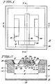
- Figure 1 is a plan view of a field effect transistor in accordance with the present invention.
- Figure 2 is a sectional view of the device of Figure 1 taken along section lines 2-2 showing the internal structure thereof.
- Figure 3 is another sectional view of a portion of the device of Figure 1 taken along section lines 3-3 thereof also showing internal structure thereof.
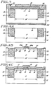
- Figures 4A-4G are schematic illustrations of vertical cross sections of a piece of semiconductor wafer in the process of fabrication of a field effect transistor in accordance with the present invention.
- Referring now to Figures 1, 2 and 3, there is shown a portion of an integrated circuit including a
field effect transistor 10 made in accordance with the present invention. The device includes a substrate of monocrystalline silicon semiconductor material of P-type conductivity and relatively high resistivity, for example, 2 ohm-cm. The substrate may be conveniently 10 mils thick. Atrench 13 about a micron wide and about a micron deep is formed in theplanar surface 12 of the substrate 11 and filled with aninsulating material 14 such as silicon dioxide surrounding anactive region 15 of the substrate isolating this region from other such regions formed in the integrated circuit substrate. The sides of theactive region 15 form a square in the plane of themajor surface 12 of the substate. Athin layer 17 of silicon dioxide is provided on theplanar surface 12. Agate electrode 18 of polycrystallinesilicon having sides insulating layer 17. Aninsulating spacer 19 having afirst side 19a, a second side 19b and a base 19c is provided.First side 19a of thespacer 19 has a height equal to the height to theside 18a of thegating electrode 18 and is contiguous therewith. The base 19c is contiguous with the top surface of the thin insulatinglayer 17. A first lightly dopedshallow region 21 of N-type conductivity is located adjacent the planar surface and underlying the base of theinsulating spacer 19 forming a PN junction 23' with the substrate. - The
insulating spacer 19 may be formed by covering the major surface of the substrate 11 with silicon dioxide, for example, by chemical vapor deposition and thereafter anisotropically etching the layer of silicon dioxide until all portions of the layer are completely removed except for aspacer 19 onside 18a of theelectrode 18 and another spacer element 20 (not shown) on theother side 18b of thegate electrode 18. Thespacer 19 is masked and spacer 20 on the other side of thegate electrode 18 is reactive ion etched using a gas such as trifluoromethane (CHF3) which does not react or reacts minimally with the polycrystalline silicon material of thegate electrode 18 and which does react with silicon dioxide thereby selectively removing theinsulating spacer 20. Thethin layer 17 of silicon dioxide is formed by thermally growing silicon dioxide in the exposed portions of the planar surface.Gate electrode 18 is formed by depositing a layer of polycrystalline silicon overlying thin insulating layer 23 and thereafter patterning the layer by photolithographic masking and etching techniques well known in the art. - A heavily doped,
deep region 25 of N-type conductivity is provided in the substrate adjacent theplanar surface 12 and forms aPN junction 26 with the substrate. ThePN junction 26 has anedge 27 in aplanar surface 12 adjacent the bottom base 19c and the side 19b of theinsulating spacer 19. An impurity or donor activator concentration in theregion 25 is substantially greater than the donor activator concentration in theregion 21. Anotherregion 28 of N-type conductivity is provided in the substrate adjacent themajor surface 12 andside 18b of thegating electrode 18 forming aPN junction 29 therewith. ThePN junction 29 has an edge in theplanar surface 12 and adjacent theside 18b of thegating electrode 18. The net impurity or donor concentration in theregion 28 of N type conductivity is substantially greater than the donor concentration of the shallow, lightly dopedregion 21 and is substantially equal to the doping concentration in theregion 25. Theregions major surface 12 of the substrate over these regions and thereafter activating the arsenic ions by heating at a suitable temperature and for a short time. - A
thick layer 30 of silicon dioxide is chemically vapor deposited on the major surface of the substrate 11. Thereafter thethick layer 30 of silicon dioxide is patterned to formopenings source region 28, thedrain region 25 and thegate electrode 18. Thereafter a layer of aluminum is sputtered over the surface of the resultant structure intoopenings source region 28, thedrain region 25 and thegate electrode 18, respectively. The device is then heated to a temperature of about 550°C for a time to bond the conductive connections of aluminum to thesource region 28, thedrain region 25 and thegate electrode 18. Subsequently, aconductive connection 35 of aluminum is formed on the opposite surface of the substrate. - Reference is now made to Figures 4A-4G which illustrate the manner of fabrication of the field effect transistor of Figures 1-3 in accordance with the present invention. Elements in Figures 4A-4G identical to elements of Figures 1-3 are identically designated. Initially, a wafer 11 of monocrystalline semiconductor material of relatively high resistivity, for example 2 ohms cm, having a convenient thickness, for example,-10 mils, and a P-type conductivity is provided. The wafer may be of any convenient diameter on which a very large number of individual field effect transistors, such as shown in Figures 1-3 may, be formed. Diagrams of Figures 4A-4G show the processing of the wafer as it affects the individual transistor on the wafer. After suitable cleaning of the surface of the wafer, a
trench 13 about 1 micron wide and about 1 micron deep is etched into the silicon substrate utilizing photolithographic masking and etching techniques well known in the art to form anactive region 15 of square outline of 3.5 microns on a side. Thereafter, the wafer is exposed to a mixture of silane and oxygen at a temperature of about 900°C for a sufficient period of time to fill thetrenches 13 with silicon dioxide and also cover the exposed surfaces 12 of the wafer of silicon. The wafer is next planarized. To this end the wafer is covered with a suitable photoresist such as Hunt type 704 photoresist. Thereafter, the resist and the silicon dioxide are reactive ion etched in an atmosphere of trifluoro-methane (CHF3) and oxygen to produce the structure shown in Figure 4A in which anactive region 15 is isolated from other active regions by theisolation regions 14 of silicon dioxide formed in the substrate 11. - In the next step of the process, shown in Figure 4B, a
layer 17 of silicon dioxide, referred to as gate oxide, is thermally grown over thesurface 12 of the substrate. A layer of polycrystalline silicon 0.5 micron thick is then deposited over the layer ofgate oxide 17. The polycrystalline layer is suitably patterned using photolithographic masking and etching techniques well known in the art to form thegate electrode 18 one micron in length fromside 18a toside 18b and 0.5 micron thick. Using thegate 18 as a mask arsenic ions of a dosage of 2x 10¹³ ions per cm2 at 100 kilovolts are implanted and then flash annealed in the substrate 11 to form lightly dopedshallow regions - In the next step of the process, shown in Figure 4C, substrate 11 is covered with a
layer 37 of chemically vapor deposited silicon dioxide 0.5 micron thick using silane and oxygen. Thereafter, thelayer 35 of silicon dioxide is anisotropically etched in trifluoromethane (CHF 3), which etches silicon dioxide at a much more rapid rate than it etches silicon, to remove the silicon dioxide from the wafer until only spacerportions spacers spacers - In the next step of the process shown in Figure 4E, a layer of photoresist is deposited over the exposed surface of the wafer covering the
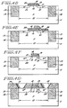
gate electrode 18, the insulatingspacers planar surface 12. The photoresist is a Shipley type AZ1470 positive photoresist 1 micron thick. The photoresist is patterned by photolithographic masking and etching techniques well known in the art to provide a mask 39 which covers a portion of thegate electrode 18, the insulatingspacer 19, and a portion of theplanar surface 12 as shown. The alignment of the mask 39 is not critical. The edge 39a of the mask 39 would be aligned to the center line of thegate electrode 18. A deviation of the alignment of edge 39a up to less than about one-half of the distance betweenedges gate electrode 18 could be tolerated. - In the next step of the process, the exposed surface of the substrate is reactive ion etched in trifluoromethane (CHF3) and argon to remove the
spacer 20 and the portion ofsilicon dioxide layer 17 beneathspacer 20, to form the structure shown in Figure 4F. Thereafter, the photoresist pattern is removed. Regions adjacent the planar surface not masked by thegate electrode 18 or the insulatingspacer 19 are implanted with arsenic ions of a dosage of 1015 atoms per cm2 at 200 kilovolts. Thereafter, the resultant structure is flash annealed at 10000C for about 10 seconds to activate the ion implants to form the deep, heavily dopedregions region 28 completely contains the lightly dopedregion 22 formed adjacent theplanar surface 12 and also heavily dopedregion 25 contains a portion of the lightly dopedregion 21 formed adjacent theplanar surface 12, as shown in Figure 4F. - The next step of the process is illustrated in Figure 4G. The surface of the wafer is covered with a
layer 30 of silicon dioxide deposited thereon by chemical vapor deposition using silane and oxygen to a thickness of about 0.5 micron. Thereafter, thelayer 30 of silicon dioxide is patterned using photolithographic masking and etching techniques well known to those skilled in the art to provideopenings source region 28 and thedrain region 25 and to provide opening 33 (Fig. 1) to thegate electrode 18. At this point in the process, metal contacts (not shown) are provided to thesource region 28, thedrain region 25 and thegate electrode 18 of the transistor formed in theactive region 15. - While the embodiments of the invention described above, N channel transistors were formed on P-type silicon substrates, P-channel transistors could as well have been formed on N-type conductivity substrates in a similar manner.
- While the invention has been described in specific embodiments, it will be understood that modifications may be made by those skilled in the art and it is intended by the appended claims to cover all such modifications and changes as fall within the true spirit and scope of the invention.
Claims (8)
Applications Claiming Priority (2)
| Application Number | Priority Date | Filing Date | Title |
|---|---|---|---|
| US60546084A | 1984-04-30 | 1984-04-30 | |
| US605460 | 1990-10-30 |
Publications (3)
| Publication Number | Publication Date |
|---|---|
| EP0160255A2 true EP0160255A2 (en) | 1985-11-06 |
| EP0160255A3 EP0160255A3 (en) | 1986-12-30 |
| EP0160255B1 EP0160255B1 (en) | 1990-06-13 |
Family
ID=24423751
Family Applications (1)
| Application Number | Title | Priority Date | Filing Date |
|---|---|---|---|
| EP85104809A Expired EP0160255B1 (en) | 1984-04-30 | 1985-04-20 | Field effect transistor device and method of making same |
Country Status (3)
| Country | Link |
|---|---|
| EP (1) | EP0160255B1 (en) |
| JP (1) | JPS60254659A (en) |
| DE (1) | DE3578270D1 (en) |
Cited By (16)
| Publication number | Priority date | Publication date | Assignee | Title |
|---|---|---|---|---|
| EP0392120A1 (en) * | 1989-04-12 | 1990-10-17 | Mitsubishi Denki Kabushiki Kaisha | Semiconductor device with a gate having asymmetric sidewalls, and a production method thereof |
| US5153683A (en) * | 1990-04-19 | 1992-10-06 | Mitsubishi Denki Kabushiki Kaisha | Field effect transistor |
| GB2273202A (en) * | 1990-04-19 | 1994-06-08 | Mitsubishi Electric Corp | Field effect transistor |
| WO1998002918A1 (en) * | 1996-07-17 | 1998-01-22 | Advanced Micro Devices, Inc. | Method for fabrication of a non-symmetrical transistor |
| WO1998010470A1 (en) * | 1996-09-03 | 1998-03-12 | Advanced Micro Devices, Inc. | Asymmetrical transistor with lightly and heavily doped drain regions and ultra-heavily doped source region |
| US5789787A (en) * | 1996-09-03 | 1998-08-04 | Advanced Micro Devices, Inc. | Asymmetrical N-channel and P-channel devices |
| US5831306A (en) * | 1996-09-03 | 1998-11-03 | Advanced Micro Devices, Inc. | Asymmetrical transistor with lightly doped drain region, heavily doped source and drain regions, and ultra-heavily doped source region |
| US5874340A (en) * | 1996-07-17 | 1999-02-23 | Advanced Micro Devices, Inc. | Method for fabrication of a non-symmetrical transistor with sequentially formed gate electrode sidewalls |
| US5877050A (en) * | 1996-09-03 | 1999-03-02 | Advanced Micro Devices, Inc. | Method of making N-channel and P-channel devices using two tube anneals and two rapid thermal anneals |
| US5904529A (en) * | 1997-08-25 | 1999-05-18 | Advanced Micro Devices, Inc. | Method of making an asymmetrical IGFET and providing a field dielectric between active regions of a semiconductor substrate |
| US5923982A (en) * | 1997-04-21 | 1999-07-13 | Advanced Micro Devices, Inc. | Method of making asymmetrical transistor with lightly and heavily doped drain regions and ultra-heavily doped source region using two source/drain implant steps |
| US6004849A (en) * | 1997-08-15 | 1999-12-21 | Advanced Micro Devices, Inc. | Method of making an asymmetrical IGFET with a silicide contact on the drain without a silicide contact on the source |
| US6027978A (en) * | 1997-01-28 | 2000-02-22 | Advanced Micro Devices, Inc. | Method of making an IGFET with a non-uniform lateral doping profile in the channel region |
| US6051471A (en) * | 1996-09-03 | 2000-04-18 | Advanced Micro Devices, Inc. | Method for making asymmetrical N-channel and symmetrical P-channel devices |
| US6096588A (en) * | 1997-11-01 | 2000-08-01 | Advanced Micro Devices, Inc. | Method of making transistor with selectively doped channel region for threshold voltage control |
| WO2009001252A1 (en) * | 2007-06-27 | 2008-12-31 | Nxp B.V. | An extended drain transistor and a method of manufacturing the same |
Citations (3)
| Publication number | Priority date | Publication date | Assignee | Title |
|---|---|---|---|---|
| DE2726003A1 (en) * | 1976-06-23 | 1977-12-29 | Hitachi Ltd | METHOD OF MAKING MIS DEVICES WITH OFFSET GATE |
| EP0014303A1 (en) * | 1979-01-24 | 1980-08-20 | Siemens Aktiengesellschaft | Method for making integrated MOS circuits by the silicon-gate technique |
| US4318216A (en) * | 1978-11-13 | 1982-03-09 | Rca Corporation | Extended drain self-aligned silicon gate MOSFET |
-
1985
- 1985-04-20 DE DE8585104809T patent/DE3578270D1/en not_active Expired - Fee Related
- 1985-04-20 EP EP85104809A patent/EP0160255B1/en not_active Expired
- 1985-04-30 JP JP60091276A patent/JPS60254659A/en active Pending
Patent Citations (3)
| Publication number | Priority date | Publication date | Assignee | Title |
|---|---|---|---|---|
| DE2726003A1 (en) * | 1976-06-23 | 1977-12-29 | Hitachi Ltd | METHOD OF MAKING MIS DEVICES WITH OFFSET GATE |
| US4318216A (en) * | 1978-11-13 | 1982-03-09 | Rca Corporation | Extended drain self-aligned silicon gate MOSFET |
| EP0014303A1 (en) * | 1979-01-24 | 1980-08-20 | Siemens Aktiengesellschaft | Method for making integrated MOS circuits by the silicon-gate technique |
Non-Patent Citations (1)
| Title |
|---|
| IEEE TRANSACTIONS ON ELECTRON DEVICES, vol. ED-29, no. 4, April 1982, pages 590-596, IEEE, New York, US; P.J. TSANG et al.: "Fabrication of high-peformance LDDFET's with oxide sidewall-spacer technology" * |
Cited By (24)
| Publication number | Priority date | Publication date | Assignee | Title |
|---|---|---|---|---|
| EP0392120A1 (en) * | 1989-04-12 | 1990-10-17 | Mitsubishi Denki Kabushiki Kaisha | Semiconductor device with a gate having asymmetric sidewalls, and a production method thereof |
| US5376812A (en) * | 1989-04-12 | 1994-12-27 | Mitsubishi Denki Kabushiki Kaisha | Semiconductor device |
| US5153683A (en) * | 1990-04-19 | 1992-10-06 | Mitsubishi Denki Kabushiki Kaisha | Field effect transistor |
| US5296398A (en) * | 1990-04-19 | 1994-03-22 | Mitsubishi Denki Kabushiki Kaisha | Method of making field effect transistor |
| GB2273202A (en) * | 1990-04-19 | 1994-06-08 | Mitsubishi Electric Corp | Field effect transistor |
| US5344788A (en) * | 1990-04-19 | 1994-09-06 | Mitsubishi Denki Kabushiki Kaisha | Method of making field effect transistor |
| GB2273202B (en) * | 1990-04-19 | 1994-10-12 | Mitsubishi Electric Corp | Field effect transistor and production method thereof |
| US5510280A (en) * | 1990-04-19 | 1996-04-23 | Mitsubishi Denki Kabushiki Kaisha | Method of making an asymmetrical MESFET having a single sidewall spacer |
| US5874340A (en) * | 1996-07-17 | 1999-02-23 | Advanced Micro Devices, Inc. | Method for fabrication of a non-symmetrical transistor with sequentially formed gate electrode sidewalls |
| WO1998002918A1 (en) * | 1996-07-17 | 1998-01-22 | Advanced Micro Devices, Inc. | Method for fabrication of a non-symmetrical transistor |
| US6051471A (en) * | 1996-09-03 | 2000-04-18 | Advanced Micro Devices, Inc. | Method for making asymmetrical N-channel and symmetrical P-channel devices |
| US6504218B1 (en) | 1996-09-03 | 2003-01-07 | Advanced Micro Devices, Inc. | Asymmetrical N-channel and P-channel devices |
| US5789787A (en) * | 1996-09-03 | 1998-08-04 | Advanced Micro Devices, Inc. | Asymmetrical N-channel and P-channel devices |
| US5877050A (en) * | 1996-09-03 | 1999-03-02 | Advanced Micro Devices, Inc. | Method of making N-channel and P-channel devices using two tube anneals and two rapid thermal anneals |
| US5831306A (en) * | 1996-09-03 | 1998-11-03 | Advanced Micro Devices, Inc. | Asymmetrical transistor with lightly doped drain region, heavily doped source and drain regions, and ultra-heavily doped source region |
| WO1998010470A1 (en) * | 1996-09-03 | 1998-03-12 | Advanced Micro Devices, Inc. | Asymmetrical transistor with lightly and heavily doped drain regions and ultra-heavily doped source region |
| US6078080A (en) * | 1996-09-03 | 2000-06-20 | Advanced Micro Devices, Inc. | Asymmetrical transistor with lightly and heavily doped drain regions and ultra-heavily doped source region |
| US6027978A (en) * | 1997-01-28 | 2000-02-22 | Advanced Micro Devices, Inc. | Method of making an IGFET with a non-uniform lateral doping profile in the channel region |
| US5923982A (en) * | 1997-04-21 | 1999-07-13 | Advanced Micro Devices, Inc. | Method of making asymmetrical transistor with lightly and heavily doped drain regions and ultra-heavily doped source region using two source/drain implant steps |
| US6004849A (en) * | 1997-08-15 | 1999-12-21 | Advanced Micro Devices, Inc. | Method of making an asymmetrical IGFET with a silicide contact on the drain without a silicide contact on the source |
| US5904529A (en) * | 1997-08-25 | 1999-05-18 | Advanced Micro Devices, Inc. | Method of making an asymmetrical IGFET and providing a field dielectric between active regions of a semiconductor substrate |
| US6096588A (en) * | 1997-11-01 | 2000-08-01 | Advanced Micro Devices, Inc. | Method of making transistor with selectively doped channel region for threshold voltage control |
| WO2009001252A1 (en) * | 2007-06-27 | 2008-12-31 | Nxp B.V. | An extended drain transistor and a method of manufacturing the same |
| US8216908B2 (en) | 2007-06-27 | 2012-07-10 | Nxp B.V. | Extended drain transistor and method of manufacturing the same |
Also Published As
| Publication number | Publication date |
|---|---|
| EP0160255A3 (en) | 1986-12-30 |
| EP0160255B1 (en) | 1990-06-13 |
| JPS60254659A (en) | 1985-12-16 |
| DE3578270D1 (en) | 1990-07-19 |
Similar Documents
| Publication | Publication Date | Title |
|---|---|---|
| US4796070A (en) | Lateral charge control semiconductor device and method of fabrication | |
| US4503601A (en) | Oxide trench structure for polysilicon gates and interconnects | |
| KR100592401B1 (en) | Self-aligned Power Field Effect Transistors in Silicon Carbide | |
| US4546536A (en) | Fabrication methods for high performance lateral bipolar transistors | |
| US3931674A (en) | Self aligned CCD element including two levels of electrodes and method of manufacture therefor | |
| US4346512A (en) | Integrated circuit manufacturing method | |
| US4749441A (en) | Semiconductor mushroom structure fabrication | |
| EP0160255B1 (en) | Field effect transistor device and method of making same | |
| JP2503460B2 (en) | Bipolar transistor and manufacturing method thereof | |
| US4001860A (en) | Double diffused metal oxide semiconductor structure with isolated source and drain and method | |
| EP0083784B1 (en) | Procedure for manufacturing integrated circuit devices having sub-micrometer dimension elements, and resulting structure | |
| US4598461A (en) | Methods of making self-aligned power MOSFET with integral source-base short | |
| US4561168A (en) | Method of making shadow isolated metal DMOS FET device | |
| US4413401A (en) | Method for making a semiconductor capacitor | |
| US4379001A (en) | Method of making semiconductor devices | |
| US4536782A (en) | Field effect semiconductor devices and method of making same | |
| US4586240A (en) | Vertical IGFET with internal gate and method for making same | |
| JPS6318673A (en) | Manufacture of semiconductor device | |
| US4473941A (en) | Method of fabricating zener diodes | |
| US4826782A (en) | Method of fabricating aLDD field-effect transistor | |
| US4001048A (en) | Method of making metal oxide semiconductor structures using ion implantation | |
| US4290186A (en) | Method of making integrated semiconductor structure having an MOS and a capacitor device | |
| CA1136290A (en) | Method of making fet | |
| US4523368A (en) | Semiconductor devices and manufacturing methods | |
| KR950003916B1 (en) | Orthogonal bipolar tr. |
Legal Events
| Date | Code | Title | Description |
|---|---|---|---|
| PUAI | Public reference made under article 153(3) epc to a published international application that has entered the european phase |
Free format text: ORIGINAL CODE: 0009012 |
|
| AK | Designated contracting states |
Designated state(s): DE FR GB NL |
|
| PUAL | Search report despatched |
Free format text: ORIGINAL CODE: 0009013 |
|
| AK | Designated contracting states |
Kind code of ref document: A3 Designated state(s): DE FR GB NL |
|
| 17P | Request for examination filed |
Effective date: 19870515 |
|
| 17Q | First examination report despatched |
Effective date: 19880930 |
|
| GRAA | (expected) grant |
Free format text: ORIGINAL CODE: 0009210 |
|
| AK | Designated contracting states |
Kind code of ref document: B1 Designated state(s): DE FR GB NL |
|
| ET | Fr: translation filed | ||
| REF | Corresponds to: |
Ref document number: 3578270 Country of ref document: DE Date of ref document: 19900719 |
|
| PLBE | No opposition filed within time limit |
Free format text: ORIGINAL CODE: 0009261 |
|
| STAA | Information on the status of an ep patent application or granted ep patent |
Free format text: STATUS: NO OPPOSITION FILED WITHIN TIME LIMIT |
|
| PG25 | Lapsed in a contracting state [announced via postgrant information from national office to epo] |
Ref country code: GB Effective date: 19910420 |
|
| 26N | No opposition filed | ||
| PG25 | Lapsed in a contracting state [announced via postgrant information from national office to epo] |
Ref country code: NL Effective date: 19911101 |
|
| NLV4 | Nl: lapsed or anulled due to non-payment of the annual fee | ||
| GBPC | Gb: european patent ceased through non-payment of renewal fee | ||
| PG25 | Lapsed in a contracting state [announced via postgrant information from national office to epo] |
Ref country code: FR Effective date: 19911230 |
|
| PG25 | Lapsed in a contracting state [announced via postgrant information from national office to epo] |
Ref country code: DE Effective date: 19920201 |
|
| REG | Reference to a national code |
Ref country code: FR Ref legal event code: ST |