EP0155008A2 - Digital filter circuit for dividing signals into subbands - Google Patents
Digital filter circuit for dividing signals into subbands Download PDFInfo
- Publication number
- EP0155008A2 EP0155008A2 EP85103027A EP85103027A EP0155008A2 EP 0155008 A2 EP0155008 A2 EP 0155008A2 EP 85103027 A EP85103027 A EP 85103027A EP 85103027 A EP85103027 A EP 85103027A EP 0155008 A2 EP0155008 A2 EP 0155008A2
- Authority
- EP
- European Patent Office
- Prior art keywords
- wave digital
- digital filter
- signals
- sampling rate
- filters
- Prior art date
- Legal status (The legal status is an assumption and is not a legal conclusion. Google has not performed a legal analysis and makes no representation as to the accuracy of the status listed.)
- Granted
Links
- 238000005070 sampling Methods 0.000 claims description 12
- 230000033764 rhythmic process Effects 0.000 claims 1
- 239000011159 matrix material Substances 0.000 description 9
- 238000000034 method Methods 0.000 description 6
- 230000005540 biological transmission Effects 0.000 description 4
- 230000000694 effects Effects 0.000 description 3
- 230000004048 modification Effects 0.000 description 3
- 238000012986 modification Methods 0.000 description 3
- 230000008569 process Effects 0.000 description 3
- 230000008901 benefit Effects 0.000 description 2
- 238000010586 diagram Methods 0.000 description 2
- 230000015572 biosynthetic process Effects 0.000 description 1
- 230000000295 complement effect Effects 0.000 description 1
- 230000001934 delay Effects 0.000 description 1
- 238000012938 design process Methods 0.000 description 1
- 238000001914 filtration Methods 0.000 description 1
- 230000010363 phase shift Effects 0.000 description 1
- 230000009467 reduction Effects 0.000 description 1
- 230000000717 retained effect Effects 0.000 description 1
- 238000000926 separation method Methods 0.000 description 1
- 238000001228 spectrum Methods 0.000 description 1
- 238000003786 synthesis reaction Methods 0.000 description 1
- 230000017105 transposition Effects 0.000 description 1
- 239000013598 vector Substances 0.000 description 1
Images


Classifications
-
- H—ELECTRICITY
- H03—ELECTRONIC CIRCUITRY
- H03H—IMPEDANCE NETWORKS, e.g. RESONANT CIRCUITS; RESONATORS
- H03H17/00—Networks using digital techniques
- H03H17/02—Frequency selective networks
- H03H17/0201—Wave digital filters
Definitions
- the invention relates to a digital filter arrangement according to the preamble of patent claim 1.
- the source signal is broken down into subbands using a filter bank. These subbands are transmitted in coded form, e.g. ADPCM, and decoded at the location of the sink and reconstructed in another filter bank. It is a so-called subband coding, for which the term "subband coding" has also become established in English. Details on this can be found, for example, in the magazine BSTJ 1981, pages 1633 to 1653. Transversal (FIR) filters are used there to implement the filter banks. However, it turns out that secondary conditions (quadrature - mirror filters) to be met for distortion-free transmission are only approximately met.
- FIR Transversal
- the invention has for its object to significantly reduce the technical complexity of these known circuits and to ensure a distortion-free transmission; circuits are therefore specified using digital wave filters with which these conditions can be met.
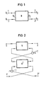
- a wave digital filter N is shown again for better understanding, the inputs of which are designated 1 and 2 and the input signals A 1 and A 2 occur there accordingly.
- the output signals B 1 and B2 appear at the connections 1 'and 2', the gate resistors R 1 and R 2 are indicated between the gates. Details of such wave digital filters can be found, for example, in the literature references in the accompanying bibliography, in particular in AEÜ 25, 79-89, 1971.
- two wave digital filters are connected, namely a wave digital filter N and a wave digital filter N T.
- the input lines 1 and 2 and the output lines 1 'and 2' can again be seen.
- the outputs of the wave digital filter N are now, so to speak, fed to the inputs of the wave digital filter N T , with a sign inverter (-1) I being connected in one of the connecting lines.
- These lines now lead to the inputs of the wave digital filter N T and its outputs are connected to the outputs 1 'and 2' of the overall circuit.
- the one output of the wave digital filter N T in the exemplary embodiment the output leading to the output line 2 ', in turn contains a sign inverter (-1) I.
- the wave digital filter N can and must be described by a scattering matrix S. then the wave digital filter N T have the scattering matrix S T.
- the input signals are denoted by a 1 and a 2 and the output signals by b 1 and b 2 .
- the further details are functional details which also refer directly to FIG. 1 and which will be discussed later.
- the circuit of FIG. 3 is practically identical to that of FIG. 2, but the multipliers u (n) and v (n) are also connected to the wave digital filter N T. To indicate this, the input signals are designated c 1 and c 2 there .
- FIG. 4 A possible modification is shown in FIG. 4, where it can be seen that the output signals b 1 and b 2 are connected together via inverters (-1) n and a subsequent summer to form the output signal d (nT).
- the individual circuit paths are connected to one another via the adders marked “plus”, delay elements of delay time T or 2T are also provided, and finally the multipliers already mentioned ( ⁇ 1 , ⁇ 2 , ⁇ 3 ) are also included.
- the input paths LP and HP can also be seen, and the combination at the output takes place via a multiplier with the coefficient 0.5.
- Some of the adders can also be replaced by subtractors, as indicated by the minus sign.
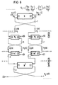
- FIG. 6 shows a wave digital filter N, which is followed by two further wave digital filters N1.
- the combination of the output signals b 1 and b 2 also takes place here to a certain extent via a “cross-connection” for the signal b 2 via a sign inverter “-1”.
- Multipliers u (n) and v (n) are connected to the other connecting lines, at which signals c 1 and c 2 then occur.
- the signals c 1 and c 2 are fed to the first inputs of the wave digital filter N 1 , the second input of which receives no input signal (0).
- An inverter (-1) then follows again in one of the output lines and multipliers u 1 (n), v 1 (n) then follow.
- the transmission circuit is now complete.
- the signals must now be assembled in the opposite order using the transposed wave digital filters N 1 T or N. This happens to a certain extent in the opposite order, each with the connection of inverters "-1", but without the use of multipliers, and the output signal b 2 (nT) is then present at one output of the transposed wave digital filter N.
- FIG. 7 An interpolating filter circuit is shown in FIG. 7, the inputs being labeled 1A, 2A, 3A and 4A.
- the exit . is marked with E.
- this is also a possible overall circuit in which corresponding further multipliers are then also required.
- These multipliers are designated g 1 to g 5 there , the individual functions can be found directly in the associated circuit diagram. Only further delay elements with the delay time 4T have to be used, which can also be found in the circuit.
- a wave digital filter (WDF) two-port has two input and two output connections. If this is used appropriately and a wave digital filter is connected to its transposed wave digital filter, the filter effect is completely compensated for, with the exception of an all-pass phase, and this is independent of selectivity requirements. This point of view also applies if every second sample at the connection points is reduced to zero, provided that a certain condition, which is easy to meet, is fulfilled. Very effective solutions are then possible.
- the method is of particular interest, for example, for subband coding.
- WVDFs wave digital filters
- WVDFs wave digital filters
- connections gates each of which consists of an input and an output connection 1.2 J.
- a conventional filter represents a two-port, so to speak
- a conventional wave digital filter has two input terminals and two output terminals.
- the filter have complementary transmission characteristics [3 to 6]
- the following figures show how some other interesting characteristics can be obtained by connecting two or more wave digital filters together, making use of the fact that each of these wave digital filters does more than just has one connection and more than one output.
- the design process can be repeated as often as required.
- the method can be used to achieve an exact solution to the problem for so-called quadrature mirror filters according to references [9] to [12], which are used in subband coding circuits [10, 11, 13 (subband coding)].
- N T can be derived from N by using flow reversal [14]. Specifically, the values of the multiplier coefficients in N D are then the same as in N, that is, for a given N, the corresponding N T can be obtained without approximation.
- S and S T It can therefore be shown that Equation 4 also applies in which As already explained in FIG. 2, the left side of equation (4) can be regarded as the scatter matrix of the overall circuit shown there. For this arrangement, the transfer function from the connections 1 to 2 'and from the connections 1' to 2 are thus zero and thus from the connections 1 to 1 'and from 2 to 3' are both det S.
- equation (2) the transfer function from the connections 1 to 2 'and from the connections 1' to 2 are thus zero and thus from the connections 1 to 1 'and from 2 to 3' are both det S.
- the circuit of FIG. 3 differs from the circuit of FIG. 2 in that the additional multipliers u (n) and v (n) are switched on. to halve the sampling rate in the special embodiment of FIG. 3.
- the functions u (n) and v (n) alternately assume the values 1 and zero and are thus either in phase or in opposite phase. This can be represented according to equations (8) and (9). It is also applies and thus the following values result for the signals c 1 and c 2
- Equation 15 holds the output signal at the output terminal 1 'contains no other frequency components than the input signal. This result is also retained, regardless of the design of the wave digital filter N, and even if this wave digital filter, for example, only fulfills very low separation requirements for the original signal in individual frequency bands, regardless of the fact that every second sample value is set to zero by the use the multipliers u (n) and v (n). The reconstructed signal is therefore available in inverted or non-inverted form at one of the outputs 2 'or 1'.
- the output signals b 1 (nT) and b 2 (nT) of the circuit of FIG. 3 are combined to form a new output signal d (nT) in the adder identified there by "+".
- the output signal b 2 runs via a sign inverter (-1) n .
- the value of the output signal d (nT) can thus be doubled.
- the above can be used directly for the circuit shown in FIG. 6.
- the crossover output signals c 1 and c 2 which are reduced in their sampling rate, are frequency-divided via further wave digital filters N 1 and, in turn, their sampling rate is reduced.
- the multipliers u 1 , v 1 must accordingly be provided there.
- these signals are processed further via the transposed wave digital filter N 1 T and combined in the output-side wave digital filter N T , so that the output signal b 2 (nT) can be taken there after the inverter (-1).
- the dimensioning method specified here has the advantage that an exact amplitude reproduction of the spectrum of the original signal is achieved even if the coefficients are rounded in an arbitrary manner.
Landscapes
- Physics & Mathematics (AREA)
- Engineering & Computer Science (AREA)
- Computer Hardware Design (AREA)
- Mathematical Physics (AREA)
- Compression, Expansion, Code Conversion, And Decoders (AREA)
- Complex Calculations (AREA)
- Transmission Systems Not Characterized By The Medium Used For Transmission (AREA)
- Dc Digital Transmission (AREA)
- Reduction Or Emphasis Of Bandwidth Of Signals (AREA)
Abstract
Description
Die Erfindung betrifft eine digitale Filteranordnung gemäß dem Oberbegriff des Patentanspruches 1.The invention relates to a digital filter arrangement according to the preamble of
Zur Bitratenreduktion von Sprachsignalen wird das Quellensignal mit Hilfe einer Filterbank in Teilbänder zerlegt. Diese Teilbänder werden .codiert übertragen, z.B. ADPCM, und am Ort der Senke decodiert und in einer weiteren Filterbank wieder rekonstruiert. Es handelt sich dabei um eine sogenannte Teilbandcodierung, für die sich im englischen Sprachgebrauch auch der Ausdruck " subbandcoding" eingebürgert hat. Einzelheiten hierüber finden sich beispielsweise in der Zeitschrift BSTJ 1981, Seiten 1633 bis 1653. Es werden dort Transversal (FIR)-Filter zur Realisierung der Filterbänke verwendet. Allerdings zeigt sich, daß zur verzerrungsfreien Übertragung zu erfüllende Nebenbedingungen (quadratur - mirror-filters) nur näherungsweise erfüllt werden.To reduce the bit rate of speech signals, the source signal is broken down into subbands using a filter bank. These subbands are transmitted in coded form, e.g. ADPCM, and decoded at the location of the sink and reconstructed in another filter bank. It is a so-called subband coding, for which the term "subband coding" has also become established in English. Details on this can be found, for example, in the magazine BSTJ 1981, pages 1633 to 1653. Transversal (FIR) filters are used there to implement the filter banks. However, it turns out that secondary conditions (quadrature - mirror filters) to be met for distortion-free transmission are only approximately met.
Der Erfindung liegt die Aufgabe zugrunde, den technischen Aufwand dieser bekannten Schaltungen erheblich zu reduzieren und eine möglichst verzerrungsfreie Übertragung zu gewährleisten; es werden deshalb Schaltungen unter Verwendung von Wellendigitalfiltern angegeben, mit denen sich diese Bedingungen erfüllen lassen.The invention has for its object to significantly reduce the technical complexity of these known circuits and to ensure a distortion-free transmission; circuits are therefore specified using digital wave filters with which these conditions can be met.
Ausgehend von der eingngs genannten digitalen Filteranordnung wird diese Aufgabe gemäß der Erfindung nach den kennzeichnenden Merkmalen des Patentanspruches 1 gelöst.Starting from the digital filter arrangement mentioned at the outset, this object is achieved according to the invention according to the characterizing features of
Vorteilhafte Ausgestaltungen sind in den Unteransprüchen angegeben.Advantageous refinements are specified in the subclaims.
Anhand von Ausführungsbeispielen wird nachstehend die Erfindung noch näher erläutert.The invention is explained in more detail below on the basis of exemplary embodiments.
Es zeigen in der Zeichnung
- Fig. 1 ein Zweitor-Wellendigitalfilter N;
- Fig. 2 die linke Seite von Gleichung(4)unter Zuschaltung eines weiteren Wellendigitalfilters mit der transponierten Streumatrix ST;
- Fig. 3 eine Anordnung wie in
Figur 2, aber mter Verwendung von Multiplizierern zur Halbierung der Abtastrate; - Fig. 4 eine Modifikation des Ausganges der Schaltung von Fig. 3;
- Fig. 3 die Realisierung eines 7 Grad Wellendigitalfilters das nur drei Multiplizierer benötigt;
- Fig. 6 eine weitere Ausgestaltung unter Verwendung von Wellendigitalfiltern N und N1 und transponierten Wellendigitalfiltern N1 T und NT;
- Fig. 7 die schaltungsmäßige Ausgestaltung einer interpolierenden Synthese-Filterbank unter Angabe der
zugehörigen Koeffizienten 1 bis 5.
- 1 shows a two-port digital wave filter N;
- 2 shows the left side of equation (4) with the connection of a further wave digital filter with the transposed scattering matrix S T ;
- 3 shows an arrangement as in FIG. 2, but with the use of multipliers for halving the sampling rate;
- Fig. 4 shows a modification of the output of the circuit of Fig. 3;
- 3 shows the implementation of a 7 degree wave digital filter that only requires three multipliers;
- 6 shows a further embodiment using wave digital filters N and N1 and transposed wave digital filters N 1 T and N T ;
- 7 shows the circuit configuration of an interpolating synthesis filter bank, specifying the
associated coefficients 1 to 5.
In Fig. 1 ist zum besseren Verständnis nochmal ein Wellendigitalfilter N dargestellt, dessen Eingänge mit 1 und 2 bezeichnet sind und es treten dort entsprechend die Eingangssignale A1 und A2 auf. An den Anschlüssen 1' und 2' treten die Ausgangssignale B1 und B2 auf, zwischen den Toren sind die Torwiderstände R1 und R2 kenntlich gemacht. Einzelheiten über solche Wellendigitalfilter finden -sich beispielsweise in den Literaturstellen des beigefügten Literaturverzeichnisses, insbesondere in AEÜ 25, 79-89, 1971.In FIG. 1, a wave digital filter N is shown again for better understanding, the inputs of which are designated 1 and 2 and the input signals A 1 and A 2 occur there accordingly. The output signals B 1 and B2 appear at the connections 1 'and 2', the gate resistors R 1 and R 2 are indicated between the gates. Details of such wave digital filters can be found, for example, in the literature references in the accompanying bibliography, in particular in AEÜ 25, 79-89, 1971.
In Fig. 2 sind zwei Wellendigitalfilter geschaltet und zwar ein Wellendigitalfilter N und ein Wellendigitalfilter NT. Es sind wiederum zu erkennen die Eingangsleitungen 1 und 2 sowie die Ausgangsleitungen 1' und 2'. Die Ausgänge des Wellendigitalfilters N werden nun gewissermaßen sich überkreuzend den Eingängen des Wellendigitalfilters NT zugeführt, wobei in der einen Verbindungsleitungen ein Vorzeicheninverter (-1) I zugeschaltet ist. Diese Leitungen führen nun auf die Eingänge des Wellendigitalfilters NT und es sind dessen Ausgänge mit den Ausgängen 1' und 2' der Gesamtschaltung verbunden. Der eine Ausgang des Wellendigitalfilters NT, im Ausführungsbeispiel der auf die Ausgangsleitung 2' führende Ausgang, enthält wiederum einen Vorzeicheninverter (-1) I. Allgemein sei noch darauf hingewiesen, daß z.B. das Wellendigitalfilter N durch eine Streumatrix S beschrieben werden kann und es muß dann das Wellendigitalfilter NT die Streumatrix ST haben.In Fig. 2, two wave digital filters are connected, namely a wave digital filter N and a wave digital filter N T. The
Im Ausführungsbeispiel von Fig. 3 sind die Eingangssignale mit a1 und a2 und die Ausgangssignale mit b1 und b2 bezeichnet. Die weiteren Angaben sind Funktionsangaben, die unmittelbar auch auf Figur 1 Bezug nehmen und auf die später noch eingegangen wird. Die Schaltung von Fig. 3 ist mit der von Fig. 2 praktisch identisch, jedoch werden dem Wellendigitalfilter NT noch die Multiplizierer u(n) und v(n) zugeschaltet. Um dies kenntlich zu machen, sind die Eingangssignale dort mit c1 und c2 bezeichnet.In the exemplary embodiment of FIG. 3, the input signals are denoted by a 1 and a 2 and the output signals by b 1 and b 2 . The further details are functional details which also refer directly to FIG. 1 and which will be discussed later. The circuit of FIG. 3 is practically identical to that of FIG. 2, but the multipliers u (n) and v (n) are also connected to the wave digital filter N T. To indicate this, the input signals are designated c 1 and c 2 there .
Eine mögliche Modifikation ist in Fig. 4 gezeichnet, wo zu erkennen ist, daß die Ausgangssignale b1 und b2 über Invertierer (-1)n und einen nachfolgenden Summierer zum Ausgangssignal d(nT) zusammengeschaltet sind.A possible modification is shown in FIG. 4, where it can be seen that the output signals b 1 and b 2 are connected together via inverters (-1) n and a subsequent summer to form the output signal d (nT).
In Fig. 5 ist die mögliche Realisierung eines Wellendigitalfilters vom Grad 7 gezeigt, bei dem nur drei Multiplizierer mit den Multiplikationskoeffizienten (γ1, γ2 und γ3) erforderlich sind.5 shows the possible realization of a wave digital filter of grade 7, in which only three multipliers with the multiplication coefficients (γ 1 , γ 2 and γ 3 ) are required.
Die einzelnen Schaltungspfade werden über die mit "Plus" gekennzeichneten Addierer miteinander verbunden, weiterhin sind noch Verzögerungsglieder der Verzögerungszeit T bzw. 2T vorgesehen und schließlich sind auch die bereits erwähnten Multiplizierer (γ1, γ2, γ3) enthalten. Zu erkennen sind ferner die Eingangspfade LP und HP, und es erfolgt die Zusammenfassung am Ausgang über einen Multiplizierer mit dem Koeffizienten 0,5. Einige der Addierer können auch durch Subtrahierer ersetzt sein, wie dies durch das Minuszeichen kenntlich gemacht ist.The individual circuit paths are connected to one another via the adders marked “plus”, delay elements of delay time T or 2T are also provided, and finally the multipliers already mentioned (γ 1 , γ 2 , γ 3 ) are also included. The input paths LP and HP can also be seen, and the combination at the output takes place via a multiplier with the coefficient 0.5. Some of the adders can also be replaced by subtractors, as indicated by the minus sign.
Im Ausführungsbeispiel von Fig. 6 ist zu erkennen ein Wellendigitalfilter N, dem zwei weitere Wellendigitalfilter N1 nachgeschaltet sind.6 shows a wave digital filter N, which is followed by two further wave digital filters N1.
Die Zusammenfassung der Ausgangssignale b1 und b2 erfolgt auch hier gewissermaßen über eine"Kreuzschaltung"beim Signal b2 noch über einen Vorzeicheninverter "-1". Den weiteren Verbindungsleitungen sind zugeschaltet Multiplizierer u(n) und v(n), an denen dann die Signale c1 und c2 auftreten. Die Signale c1 bzw. c2 werden den ersten Eingängen des Wellendigitalfilters N1 zugeführt, dessen zweiter Eingang kein Eingangssignal (0) erhält. In einer der Ausgangsleitungen folgt dann wieder ein Invertierer (-1) und es folgen anschließend die Multiplizierer u1 (n), v1(n). Damit ist die sendeseitige Schaltung vollständig. Auf der empfängerseitigen Seite müssen nun die Signale in entgegengesetzer Reihenfolge über die transponierten Wellendigitalfilter N1T bzw. N zusammengesetzt werden. Es geschieht dies gewissermaßen in entgegengesetzer Reihenfolge, jeweils unter Zuschaltung von Invertern "-1", jedoch ohne Verwendung von Multiplizierern und es ist dann an dem einen Ausgang des transponierten Wellendigitalfilters N das Ausgangssignal b2 (nT) vorhanden.The combination of the output signals b 1 and b 2 also takes place here to a certain extent via a “cross-connection” for the signal b 2 via a sign inverter “-1”. Multipliers u (n) and v (n) are connected to the other connecting lines, at which signals c 1 and c 2 then occur. The signals c 1 and c 2 are fed to the first inputs of the wave digital filter N 1 , the second input of which receives no input signal (0). An inverter (-1) then follows again in one of the output lines and multipliers u 1 (n), v 1 (n) then follow. The transmission circuit is now complete. On the receiver side, the signals must now be assembled in the opposite order using the transposed wave digital filters N 1 T or N. This happens to a certain extent in the opposite order, each with the connection of inverters "-1", but without the use of multipliers, and the output signal b 2 (nT) is then present at one output of the transposed wave digital filter N.
In Fig. 7 ist eine interpolierende Filterschaltung gezeigt, die Eingänge sind mit 1A, 2A, 3A und 4A bezeichnet sind. Der Ausgang . ist mit E bezeichnet. Wie in Fig. 5 handelt es sich auch hier um eine mögliche Gesamtschaltung, bei der dann auch entsprechende weitere Multiplizierer benötigt werden. Diese Multiplizierer sind dort mit g1 bis g5 bezeichnet, die einzelnen Funktionen können unmittelbar dem zugehörigen Schaltbild entnommen werden. Es müssen lediglich weitere Verzögerungsglieder mit der Verzögerungszeit 4T verwendet werden, was ebenfalls der Schaltung entnommen werden kann.An interpolating filter circuit is shown in FIG. 7, the inputs being labeled 1A, 2A, 3A and 4A. The exit . is marked with E. As in FIG. 5, this is also a possible overall circuit in which corresponding further multipliers are then also required. These multipliers are designated g 1 to g 5 there , the individual functions can be found directly in the associated circuit diagram. Only further delay elements with the
Zur weiteren Erläuterung sei noch folgendes ausgeführt.To further explain the following.
Ein Wellendigitalfilter (WDF) Zweitor hat zwei Eingangs - und zwei Ausgangsanschlüsse. Wenn man dies in geeigneter Weise benutzt und ein Wellendigitalfilter mit seinem transponierten Wellendigitalfilter verbindet, ist die Filterwirkung vollständig kompensiert mit Ausnahme von einer Allpaßphase, und dies unabhängig von Selektivitätsforderungen. Dieser Gesichtspunkt trifft auch dann zu, wenn an den Verbindungspunkten jede zweite Abtastprobe auf Null reduziert ist, vorausgesetzt, daß eine bestimmte Bedingung, die jedoch leicht einzuhalten ist, erfüllt ist. Sehr wirkungsvolle Lösungen sind dann möglich.A wave digital filter (WDF) two-port has two input and two output connections. If this is used appropriately and a wave digital filter is connected to its transposed wave digital filter, the filter effect is completely compensated for, with the exception of an all-pass phase, and this is independent of selectivity requirements. This point of view also applies if every second sample at the connection points is reduced to zero, provided that a certain condition, which is easy to meet, is fulfilled. Very effective solutions are then possible.
Die Methode ist beispielsweise besonders bei der Teilbandcodierung von Interesse.The method is of particular interest, for example, for subband coding.
Einer der interessierenden Aspekte von Wellendigitalfiltern (WVDFs) ist, daß sie tatsächlich über Tore zugänglich sind, das heißt also über Anschlußtore, von denen jedes aus einem Eingangs- und einem Ausgangsanschluß besteht 1,2 J. Damit stellt gewissermaßen ein herkömmliches Filter ein Zweitor dar, ein herkömmliches Wellendigitalfilter weist zwei Eingangsanschlüsse und zwei Ausgangsanschlüsse auf. Es besteht damit die Möglichkeit, daß die Filter. komplementäre Übertragungseigenschaften haben [3 bis 6) Anhand der beigefügten Figuren wird nachfolgend gezeigt, wie einige weitere interessante Eigenschaften erhalten werden können, wenn zwei oder mehr Wellendigitalfilter miteinander verbunden werden, wobei man wohl von der Tatsache Gebrauch macht, daß jedes dieser Wellendigitalfilter mehr als nur einen Anschluß und mehr als nur einen Ausgang zur Verfügung hat.One of the interesting aspects of wave digital filters (WVDFs) is that they are actually accessible via gates, that is to say via connection gates, each of which consists of an input and an output connection 1.2 J. This means that a conventional filter represents a two-port, so to speak , A conventional wave digital filter has two input terminals and two output terminals. There is a possibility that the filter. have complementary transmission characteristics [3 to 6] The following figures show how some other interesting characteristics can be obtained by connecting two or more wave digital filters together, making use of the fact that each of these wave digital filters does more than just has one connection and more than one output.
Die einfachste dieser Anordnungen wird mit Fig. 2/3 analysiert. Es wird dabei gezeigt, daß durch eine entsprechende Verbindung eines ersten Wellendigitalfilters mit seinem transponierten Wellendigitalfilter, der Filtereffekt vollständig kompensiert wird bis auf eine Allpaßübertragungsfunktion.Eine Modifikation dieser Anordnung, die eine Abtastratenerniedrigung in der Weise bewirkt, daß bei jeder zweiten Abtastprobe Nullen an den Verbindungspunkten gesetzt werden, wird dann beschrieben. Auch hier wird wiederum eine volle Kompensation mit Ausnahme von einer Allpaßfunktion erreicht, wenn das Wellendigitalfilter einer passenden Bedingung genügt. Diese Bedingung kann ohne weiteres eingehalten werden, insbesondere für symmetrische und antimetrische Filter, deren charakteristische Funktion selbstreziprok ist, in welchem Fall drastische Einsparungen der schaltungstechnischen Erfordernisse erreicht werden, insbesondere für symmetrische Filter L5 bis 8].The simplest of these arrangements is analyzed with Fig. 2/3. It is shown that a corresponding connection of a first wave digital filter to its transposed wave digital filter completely compensates for the filter effect except for an all-pass transfer function, a modification of this arrangement which causes a sampling rate reduction in such a way that zeros at the connection points for every second sample will then be described. Again, full compensation is achieved with the exception of an all-pass function if the wave digital filter meets a suitable condition. This condition can easily be met, especially for symmetrical and antimetric filters, the characteristic function of which is self-reciprocal, in which case drastic savings in circuitry requirements can be achieved, in particular for symmetrical filters L5 to 8].
Das Entwurfsverfahren läßt sich an sich beliebig oft wiederholen. Hinzu kommt, daß es möglich ist, ein Signal nach mehr oder weniger vorgegebenen Filtervorgängen in zwei individuelle Signale zu teilen, für jedes die Abtastrate zu halbieren, den gesamten Prozeß auf jedes der Teilsignale anzuwenden, diesen Prozeß so oft man es wünscht zu wiederholen und das Amplituden-Frequenz-Verhalten des Originalsignals zu rekonstruieren, selbst wenn die beteiligten Filter in den verschiedenen Schritten keine vorgegebenen Selektivitätsforderungen haben. Im speziellen ist die Methode anwendbar zur Erzielung einer exakten Lösung des Problems für sogenannte Quadratur-Spiegelfilter gemäß den Literaturstellen[9]bis[12], die in Teilbandcodierungsschaltungen [10, 11, 13 (subband-Coding)] angewendet werden.The design process can be repeated as often as required. In addition, it is possible to divide a signal into two individual signals after more or less predetermined filtering processes, to halve the sampling rate for each, to apply the entire process to each of the partial signals, to repeat this process as often as desired and that To reconstruct the amplitude-frequency behavior of the original signal, even if the filters involved in the various steps have no specified selectivity requirements. In particular, the method can be used to achieve an exact solution to the problem for so-called quadrature mirror filters according to references [9] to [12], which are used in subband coding circuits [10, 11, 13 (subband coding)].
Betrachtet sei nun anhand der Fig. 1 eine Anordnung mit einheitlicher Abtastrate und es ist dort das einleitend schon beschriebene Wellendigitalfilter N zu erkennen. Schreibt man
![]()
![]()
Nimmt man an, daß NT eine transponierte von N ist, das heißt also ein Wellendigitalfilter, für das B = ST A gilt. Bekanntlich kann NT abgeleitet werden aus N durch eine Anwendung der Flußumkehr [14] . Im einzelnen sind die Werte der Multipliziererkoeffizienten in ND dann die gleichen wie in N, das heißt für ein gegebenes N läßt sich das korrespondierende NT ohne Näherung erhalten. Für S und ST können wir dann schreiben


![]()
![]()
Es ist ansich bekannt, daß für ein verlustfreies NR det S eine Allpaßfunktion ist [15]. Die Anordnung von Fig. 2 hat also die Wirkung, daß eine Allpaß-Phasenverschiebung eingeführt wird.It is known per se that a loss-free N R det S is an all-pass function [15]. The arrangement of Fig. 2 thus has the effect of introducing an all-pass phase shift.
Wie einleitend schon erwähnt, unterscheidet sich die Schaltung von Fig. 3 von der Schaltung nach Fig. 2 durch die Einschaltung der zusätzlichen Multiplizierer u(n) und v(n). um im speziellen Ausführungsbeispiel von Fig. 3 die Abtastrate zu halbieren. Die Funktionen u(n) und v (n) nehmen abwechselnd die Werte 1 und Null an und sind so entweder in Phase oder in Gegenphase. Man kann dies gemäß Gleichungen(8)und(9)darstellen.![]()
![]()
![]()
![]()
![]()
![]()
![]()
![]()
![]()
![]()
![]()
![]()
Die Signale b1(n+T) am Ausgang 1' und b2(n+T) am Ausgang 2' gehorchen dann den Gleichungen (13)und (14)

Da Gleichung 15 gilt
In der Schaltung von Fig. 4 werden die Ausgangssignale b1 (nT) und b2(nT) der Schaltung von Fig. 3 zu einem neuen Ausgangssignal d(nT) in dem dort mit "+" kenntlich gemachten Addierer zusammengefügt. Das Ausgangssignal b2 läuft über einen Vorzeicheninverter (-1)n. Es läßt sich damit also der Wert des Ausgangssignals d(nT) verdoppeln.In the circuit of FIG. 4, the output signals b 1 (nT) and b 2 (nT) of the circuit of FIG. 3 are combined to form a new output signal d (nT) in the adder identified there by "+". The output signal b 2 runs via a sign inverter (-1) n . The value of the output signal d (nT) can thus be doubled.
Bei dem in Fig. 5 dargestellten Wellendigitalfilter vom Grad 7 sind ein Tiefpaß LP und ein Hochpaß HP zusammengeführt. Es werden nur 3 Multiplizierer benötigt, die folgende Werte haben: g1 = 0,497011990; g1 = 0,160797587; g3 = 0,169353564. Für die in Fig. 6 dargestellte Schaltung kann unmittelbar auf das Vorherstehende zurückgegriffen werden. Auf der Senderseite "Sender" werden also die in ihrer Abtastrate herabgesetzten Weichen-Ausgangssignale c1 und c2 über weitere Wellendigitalfilter N1 frequenzmäßig aufgeteilt und wiederum in ihrer Abtastrate reduziert. Entsprechend müssen dort die Multiplizierer u1, v1 vorgesehen werden. Auf der Empfängerseite "Empfänger" werden diese Signale über die transponierten Wellendigitalfilter N1 T weiterverarbeitet und im ausgangsseitigen Wellendigitalfilter NT zusammengefaßt, so daß dort nach dem Inverter (-1) das Ausgangssignal b2 (nT) abgenommen werden kann.5, a low-pass LP and a high-pass HP are merged. Only 3 multipliers are required, which have the following values: g 1 = 0.497011990; g 1 = 0.160797587; g 3 = 0.169353564. The above can be used directly for the circuit shown in FIG. 6. On the transmitter side "transmitter", the crossover output signals c 1 and c 2, which are reduced in their sampling rate, are frequency-divided via further wave digital filters N 1 and, in turn, their sampling rate is reduced. The multipliers u 1 , v 1 must accordingly be provided there. On the receiver side "receiver", these signals are processed further via the transposed wave digital filter N 1 T and combined in the output-side wave digital filter N T , so that the output signal b 2 (nT) can be taken there after the inverter (-1).
Die in Fig. 7 dargestellte Schaltung wurde an sich schon detailliert besprochen, die Multiplikationsfaktoren (1 bis 5) sind unmittelbar in der Zeichnung angegeben. Hingewiesen sei nochmals darauf, daß die dort mit T bzw. 2T bzw. 4T kenntlich gemachte Blockschaltbilder als Laufzeitverzögerungen der Laufzeit T bzw. 2T, bzw. 4T aufzufassen sind.The circuit shown in FIG. 7 has already been discussed in detail, the multiplication factors (1 to 5) are indicated directly in the drawing. It should be pointed out once again that the block diagrams identified there with T or 2T or 4T are to be interpreted as runtime delays of the runtime T or 2T or 4T.
Auch in der digitalen Technik ist es möglich, Filter zu realisieren, deren charakteristische Funktionen c (g) zueinander selbstreziprok sind bzw. bei denen auch die charakteristischen Funktionen der Referenzfilter zueinander selbstreziprok sind. Diese mathematische Bedingung ist dann erfüllt, wenn![]()
![]()
Abgesehen von den bereits genannten Vorteilen hat die hier angegebene Dimensionierungsmethode noch den Vorteil, daß eine exakte Amplitudenreproduktion des Spektrums des ursprünglichen Signals auch dann erreicht wird, wenn die Koeffizienten in willkürlicher Weise gerundet werden.Apart from the advantages already mentioned, the dimensioning method specified here has the advantage that an exact amplitude reproduction of the spectrum of the original signal is achieved even if the coefficients are rounded in an arbitrary manner.
- [1]A.Fettweis,AE0,25,79-89,1971.[1] A. Fettweis, AE 0.25.79-89.1971.
- [2]-,Lecture Notes., ECCTD, Stuttgart, Germany,1983.[2] -, Lecture Notes., ECCTD, Stuttgart, Germany, 1983.
- [3]-,Proc.Florence Seminar on Dig.Filt.,Florence,72.[3] -, Proc.Florence Seminar on Dig.Filt., Florence, 72.
- [4]M.Benanger,O.Didier,Cables et Transm.,31,497-506,1977.[4] M. Benanger, O.Didier, Cables et Transm., 31.497-506, 1977.
- [5]W.Wegener,AE0,33,239-243,1979.[5] W.Wegener, AE0.33.239-243.1979.
- [6]A.Fettweis, IEEE Trans.COM,30,1575-1586,1982. C7]J.A.Nossek,H.-O.Schwartz,Proc.ISCAS,845-848, Newport Beach,CA,1983.[6] A. Fettweis, IEEE Trans.COM, 30.1575-1586, 1982. C7] J.A. Nossek, H.-O. Schwwartz, Proc.ISCAS, 845-848, Newport Beach, CA, 1983.
- [8]K.Meerkötter, Proc. ECCTO ,217-220 ,Stuttgart,1983.[8] K.Meerkötter, Proc. ECCTO, 217-220, Stuttgart, 1983.
- [9]0.Esteban,C.Galand,Proc.ICASSP,191-195,Hartford, Conn.,1977.[9] 0.Esteban, C.Galand, Proc.ICASSP, 191-195, Hartford, Conn., 1977.
- [10]E.R.Crochiere,BSTJ,56,747-770,1977.[10] E.R. Crochiere, BSTJ, 56.747-770, 1977.
- [11]T.A.Ramstad.O.Foss,Proc.EUSIPCO,747-752,Lausanne, Switzerland,1980.[11] T.A. Ramstad.O. Foss, Proc.EUSIPCO, 747-752, Lausanne, Switzerland, 1980.
- [12]H.J.Kussbaumer,C.Galand,Proc.EUSIPCO,69-72, Erlangen,Germany,1983.[12] H.J. Kussbaumer, C.Galand, Proc.EUSIPCO, 69-72, Erlangen, Germany, 1983.
- [13]R.E.Crochiere,BSTJ,60,1633-1653,1981.[13] R.E. Crochiere, BSTJ, 60.1633-1653.1981.
- [14]A.Fettweis,Int.J.CTA,1,323-337,1973.[14] A. Fettweis, Int.J.CTA, 1,323-337,1973.
- [15]V.Belevitch,Classical Network,Theory,Holden-Oay, San Francisco,CA,1968.[15] V. Belevitch, Classical Network, Theory, Holden-Oay, San Francisco, CA, 1968.
Claims (3)
Priority Applications (1)
| Application Number | Priority Date | Filing Date | Title |
|---|---|---|---|
| AT85103027T ATE70674T1 (en) | 1984-03-16 | 1985-03-15 | DIGITAL FILTER ARRANGEMENT FOR DISTRIBUTING SIGNALS INTO SUB-BANDS. |
Applications Claiming Priority (2)
| Application Number | Priority Date | Filing Date | Title |
|---|---|---|---|
| DE3409817 | 1984-03-16 | ||
| DE3409817 | 1984-03-16 |
Publications (3)
| Publication Number | Publication Date |
|---|---|
| EP0155008A2 true EP0155008A2 (en) | 1985-09-18 |
| EP0155008A3 EP0155008A3 (en) | 1987-06-03 |
| EP0155008B1 EP0155008B1 (en) | 1991-12-18 |
Family
ID=6230789
Family Applications (1)
| Application Number | Title | Priority Date | Filing Date |
|---|---|---|---|
| EP85103027A Expired - Lifetime EP0155008B1 (en) | 1984-03-16 | 1985-03-15 | Digital filter circuit for dividing signals into subbands |
Country Status (3)
| Country | Link |
|---|---|
| EP (1) | EP0155008B1 (en) |
| AT (1) | ATE70674T1 (en) |
| DE (1) | DE3584901D1 (en) |
Cited By (3)
| Publication number | Priority date | Publication date | Assignee | Title |
|---|---|---|---|---|
| DE3627679A1 (en) * | 1986-08-14 | 1988-02-25 | Blaupunkt Werke Gmbh | FILTER ARRANGEMENT |
| GB2258963A (en) * | 1991-08-23 | 1993-02-24 | Sony Broadcast & Communication | Sub-band filters |
| EP0501690A3 (en) * | 1991-02-28 | 1993-07-21 | British Aerospace Public Limited Company | Apparatus for and method of digital signal processing |
Citations (1)
| Publication number | Priority date | Publication date | Assignee | Title |
|---|---|---|---|---|
| EP0123278A1 (en) * | 1983-04-22 | 1984-10-31 | Siemens Aktiengesellschaft | Digital wave filter with bridged digital wave filters |
-
1985
- 1985-03-15 EP EP85103027A patent/EP0155008B1/en not_active Expired - Lifetime
- 1985-03-15 DE DE8585103027T patent/DE3584901D1/en not_active Expired - Fee Related
- 1985-03-15 AT AT85103027T patent/ATE70674T1/en active
Patent Citations (1)
| Publication number | Priority date | Publication date | Assignee | Title |
|---|---|---|---|---|
| EP0123278A1 (en) * | 1983-04-22 | 1984-10-31 | Siemens Aktiengesellschaft | Digital wave filter with bridged digital wave filters |
Non-Patent Citations (2)
| Title |
|---|
| IEEE 1983 INTERNATIONAL SYMPOSIUM ON CIRCUITS AND SYSTEMS, New Port Beach, California, 2.-4. Mai 1983, Band 2, Seiten 845-848, IEEE, New York, US; J.A. NOSSEK et al.: "Wave digital lattice filters with applications in communication systems" * |
| IEEE TRANSACTIONS ON ACOUSTICS SPEECH AND SIGNAL PROCESSING, Band ASSP-30, Nr. 5, Oktober 1982, Seiten 709-718, IEEE, New York, US; L. GAZSI: "Single chip filter bank with wave digital filters" * |
Cited By (5)
| Publication number | Priority date | Publication date | Assignee | Title |
|---|---|---|---|---|
| DE3627679A1 (en) * | 1986-08-14 | 1988-02-25 | Blaupunkt Werke Gmbh | FILTER ARRANGEMENT |
| EP0501690A3 (en) * | 1991-02-28 | 1993-07-21 | British Aerospace Public Limited Company | Apparatus for and method of digital signal processing |
| GB2258963A (en) * | 1991-08-23 | 1993-02-24 | Sony Broadcast & Communication | Sub-band filters |
| US5268905A (en) * | 1991-08-23 | 1993-12-07 | Sony United Kingdom Limited | Sub band filters |
| GB2258963B (en) * | 1991-08-23 | 1995-06-14 | Sony Broadcast & Communication | Sub band filters |
Also Published As
| Publication number | Publication date |
|---|---|
| DE3584901D1 (en) | 1992-01-30 |
| EP0155008A3 (en) | 1987-06-03 |
| ATE70674T1 (en) | 1992-01-15 |
| EP0155008B1 (en) | 1991-12-18 |
Similar Documents
| Publication | Publication Date | Title |
|---|---|---|
| EP0290790B1 (en) | Filter bank | |
| DE2626122C2 (en) | Arrangement for processing signals in a frequency division multiplex transmission system | |
| EP0279208B1 (en) | Non-recursive half-band filter | |
| DE3621737C2 (en) | ||
| EP0234452B1 (en) | Digital circuit arrangement for sampling rate conversion and signal filtration, and method for making it | |
| EP0155008B1 (en) | Digital filter circuit for dividing signals into subbands | |
| EP0256286B1 (en) | Filter device | |
| DE3922469C2 (en) | ||
| EP0276394A2 (en) | Transmission arrangement for digital signals | |
| EP0075311B1 (en) | Arrangement for speech transmission based on the channel vocoder principle | |
| DE3883414T2 (en) | Digital signal processing system with a filter bank. | |
| DE3837841C1 (en) | Filter bank for the frequency-division multiplexing or frequency-division demultiplexing of channel signals | |
| DE2011772C3 (en) | Filter with a periodic frequency characteristic | |
| EP0258574A2 (en) | Filter device | |
| DE3705207C2 (en) | ||
| DE3836081C1 (en) | Filter bank for frequency multiplexing or frequency demultiplexing of channel signals | |
| EP0348393B1 (en) | Non-recursive half-band filter | |
| DE1912674A1 (en) | Digital phase equalizer | |
| EP0065648B1 (en) | Method for frequency scrambling sub-bands | |
| DE3047450A1 (en) | Filter for sampling frequency adjustment - has first stage defining blocking region and second stage adjusting transmission region of first stage | |
| DE4328497C1 (en) | Digital filter bank | |
| DE19627784C1 (en) | Non-recursive half-band filter switch with complex coefficients | |
| EP0367932A2 (en) | Filter bank for the frequency division multiplexing or demultiplexing of channel signals | |
| DE3318228C2 (en) | ||
| DE1902057C3 (en) | Method and circuit arrangement for filtering out a residual sideband signal from a double sideband signal |
Legal Events
| Date | Code | Title | Description |
|---|---|---|---|
| PUAI | Public reference made under article 153(3) epc to a published international application that has entered the european phase |
Free format text: ORIGINAL CODE: 0009012 |
|
| AK | Designated contracting states |
Designated state(s): AT BE CH DE FR GB IT LI NL SE |
|
| PUAL | Search report despatched |
Free format text: ORIGINAL CODE: 0009013 |
|
| AK | Designated contracting states |
Kind code of ref document: A3 Designated state(s): AT BE CH DE FR GB IT LI NL SE |
|
| 17P | Request for examination filed |
Effective date: 19871106 |
|
| 17Q | First examination report despatched |
Effective date: 19900420 |
|
| GRAA | (expected) grant |
Free format text: ORIGINAL CODE: 0009210 |
|
| AK | Designated contracting states |
Kind code of ref document: B1 Designated state(s): AT BE CH DE FR GB IT LI NL SE |
|
| PG25 | Lapsed in a contracting state [announced via postgrant information from national office to epo] |
Ref country code: SE Effective date: 19911218 Ref country code: NL Effective date: 19911218 Ref country code: GB Effective date: 19911218 |
|
| REF | Corresponds to: |
Ref document number: 70674 Country of ref document: AT Date of ref document: 19920115 Kind code of ref document: T |
|
| REF | Corresponds to: |
Ref document number: 3584901 Country of ref document: DE Date of ref document: 19920130 |
|
| ET | Fr: translation filed | ||
| ITF | It: translation for a ep patent filed | ||
| NLV1 | Nl: lapsed or annulled due to failure to fulfill the requirements of art. 29p and 29m of the patents act | ||
| GBV | Gb: ep patent (uk) treated as always having been void in accordance with gb section 77(7)/1977 [no translation filed] | ||
| PLBE | No opposition filed within time limit |
Free format text: ORIGINAL CODE: 0009261 |
|
| STAA | Information on the status of an ep patent application or granted ep patent |
Free format text: STATUS: NO OPPOSITION FILED WITHIN TIME LIMIT |
|
| 26N | No opposition filed | ||
| PGFP | Annual fee paid to national office [announced via postgrant information from national office to epo] |
Ref country code: AT Payment date: 19960223 Year of fee payment: 12 |
|
| PGFP | Annual fee paid to national office [announced via postgrant information from national office to epo] |
Ref country code: BE Payment date: 19960319 Year of fee payment: 12 |
|
| PGFP | Annual fee paid to national office [announced via postgrant information from national office to epo] |
Ref country code: FR Payment date: 19960328 Year of fee payment: 12 |
|
| PGFP | Annual fee paid to national office [announced via postgrant information from national office to epo] |
Ref country code: DE Payment date: 19960520 Year of fee payment: 12 |
|
| PGFP | Annual fee paid to national office [announced via postgrant information from national office to epo] |
Ref country code: CH Payment date: 19960624 Year of fee payment: 12 |
|
| PG25 | Lapsed in a contracting state [announced via postgrant information from national office to epo] |
Ref country code: AT Effective date: 19970315 |
|
| PG25 | Lapsed in a contracting state [announced via postgrant information from national office to epo] |
Ref country code: LI Effective date: 19970331 Ref country code: CH Effective date: 19970331 Ref country code: BE Effective date: 19970331 |
|
| BERE | Be: lapsed |
Owner name: SIEMENS A.G. Effective date: 19970331 |
|
| REG | Reference to a national code |
Ref country code: CH Ref legal event code: PL |
|
| PG25 | Lapsed in a contracting state [announced via postgrant information from national office to epo] |
Ref country code: FR Free format text: LAPSE BECAUSE OF NON-PAYMENT OF DUE FEES Effective date: 19971128 |
|
| PG25 | Lapsed in a contracting state [announced via postgrant information from national office to epo] |
Ref country code: DE Effective date: 19971202 |
|
| REG | Reference to a national code |
Ref country code: FR Ref legal event code: ST |