EP0153492A1 - Protection circuit for apparatus controlled by electrical signals - Google Patents
Protection circuit for apparatus controlled by electrical signals Download PDFInfo
- Publication number
- EP0153492A1 EP0153492A1 EP84116254A EP84116254A EP0153492A1 EP 0153492 A1 EP0153492 A1 EP 0153492A1 EP 84116254 A EP84116254 A EP 84116254A EP 84116254 A EP84116254 A EP 84116254A EP 0153492 A1 EP0153492 A1 EP 0153492A1
- Authority
- EP
- European Patent Office
- Prior art keywords
- protection circuit
- transistor
- reference voltage
- input
- circuit
- Prior art date
- Legal status (The legal status is an assumption and is not a legal conclusion. Google has not performed a legal analysis and makes no representation as to the accuracy of the status listed.)
- Ceased
Links
Images
Classifications
-
- H—ELECTRICITY
- H03—ELECTRONIC CIRCUITRY
- H03K—PULSE TECHNIQUE
- H03K5/00—Manipulating of pulses not covered by one of the other main groups of this subclass
- H03K5/01—Shaping pulses
- H03K5/08—Shaping pulses by limiting; by thresholding; by slicing, i.e. combined limiting and thresholding
Definitions
- the invention relates to a protective circuit for devices controlled by electrical signals, in particular analog signals, according to the preamble of the main claim.
- a protective circuit for analog and digital signals is already known from DE-OS 32 40 280. These analog and digital signals are intended for an input of a device controlled by electrical signals, which is protected against positive and / or negative overvoltage at the input by the protective circuit.
- a problem with such a protective circuit is a non-linearity of the input resistance of the device to be protected of approximately 100 millivolts per decade of the input current. This is associated with a strong temperature dependence of the input resistance, which can falsify a measurement result, for example.
- the protective circuit according to the invention has the advantage over the prior art of having a large voltage range without influencing the current of the input of the device.
- a very linear and flat course of the boundary line is achieved at the operating point.
- At the boundary point i.e. there is a very sharp, temperature-independent kink in the current-voltage characteristic at the limit voltage.
- the modulation range of the device in particular an analog-digital converter, can be brought up to a few 10 millivolts to the limiting voltage.
- the entire protective circuit consists only of semiconductor elements and is therefore easy to integrate, so that the invention finds wide fields of application in the field of integrated circuits.
- the protective circuit according to the invention can be converted into a dual structure in the simplest way, so that a protective circuit for protection against overvoltages via an upper reference voltage is converted into a protective circuit for protection against overvoltages below a lower reference voltage.
- a protective circuit for protection against overvoltages via an upper reference voltage is converted into a protective circuit for protection against overvoltages below a lower reference voltage.
- current sources are less area-intensive than high-resistance resistors.
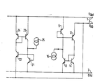
- the drawing shows a circuit design of a protective circuit according to the invention at the input of a device, not shown, controlled by electrical signals.
- the drawing shows two reference voltages: the first reference voltage U ref is at a terminal 1 and the second reference voltage Gnd at a terminal 2.
- An input voltage U AD is applied to a terminal 3 and is applied for processing in an analog-to-digital converter (not shown in more detail).
- the two reference voltages U ref and Gnd also lead to the analog-to-digital converter.
- the embodiment has two circuit halves, the right half in the drawing with the components 11 to 15 serves to protect against overvoltages that exceed the first reference voltage U ref , the left half of the circuit with the components 21 to 25 is constructed dual symmetrically to the right half of the circuit and serves to protect against voltages which are applied to terminal 3 and fall below the second reference voltage Gnd.
- a first transistor 11 and a second transistor 12 are of the PNP type and are connected to the base.
- the emitter of transistor 11 is at terminal 1, the collector and the base are connected together sen.
- the emitter of transistor 12 leads to terminal 3.
- Two npn transistors 13, 14 are also connected to the base.
- the collector of transistor 14 is connected to its base and to the collector of transistor 12.
- the collector of transistor 13 leads to the collector of transistor 11 and to a current source 15.
- the emitters of transistors 13, 14 lead to terminal 2.
- the circuit consists of two interconnected complementary current mirrors, such as are known from the magazine "Funkschau", 26/1983, pages 44 ff.
- transistor 14 represents an input transistor and transistor 13 an output transistor;
- transistor 11 is an input transistor and transistor 12 is an output transistor.
- the left half of the circuit shows a dual circuit structure to the right, where npn types are converted into pnp types.
- the two reference voltages are also exchanged topologically in a dual manner.
- the protective circuit on the left half of the drawing in addition to the dual structure, also has a corresponding electrical behavior, so that only the right circuit structure is explained below.
- the numbering is chosen such that the dual transistor receives the number 21 for the transistor 11, the dual transistor & the number 22 for the transistor 12, etc.
- the transistor 12 becomes conductive.
- An input current flows from the terminal 3 into the transistor 12, and thus as a collector current in a current mirror, which is formed from the transistors 13, 14.
- the collector current of transistor 13 thus has the same size as that of transistor 12.
- This current mirroring causes an increase in the emitter-collector voltage at transistor 11, so that the emitter potential of transistor 12, and thus the input potential at terminal 3, regardless of the input current the reference voltage U ref cannot exceed.
- the transistors 11, 13, 14 thus carry out a voltage regulation at the terminal 3 via the input current, as long as the output voltage of a driving circuit connected to the terminal 3 is greater than U ref .
- the input current into terminal 3 is therefore only determined by the output resistance of the driving circuit.
- the symmetrical structure of the transistors 11, 12 to the transistors 13, 14 brings about an excellent temperature compensation of the limiter threshold at a temperature drift of the input current of less than about 0.2 / uA / 100 ° C.
- the protective circuit according to the invention can be easily integrated within an integrated circuit.
- the implementation of the current sources 15, 25 does not pose any problems.
- the two current sources 15, 25 can also be replaced in a simple manner by a single high-resistance resistor on the order of one megohm, this resistance between the collector of the transistor 13 and the collector of transistor 23 is switched.
- This resistor can be implemented as a field-effect transistor within an integrated module.
- the use of transistors with multiple emitters is of course within the scope of the invention, for example to change the mirror factor.
- Fast pnp structures are advantageously used to increase the cut-off frequency of the protective circuit.
Abstract
Es wird eine Schutzschaltung für durch elektrische Signale, insbesondere analoge Signale, gesteuerte Geräte vorgeschlagen, deren Eingang (3) gegen positive und/oder negative Überspannung gegenüber einer oberen Bezugsspannung (1) und/oder unteren Bezugspannung (2) gesichert wird. Durch eine Kollektorstromregelung des Transistors (12) am Eingang (3) durch drei Transistoren (11, 13, 14) wird das Potential des Eingangs (3) auf dem Bezugspannungspotential gehalten, solange eine treibende Schaltung eine Überspannung liefert. Eine dual aufgebaute Schaltung (21 bis 24) bietet die Sicherung gegenüber einer negativen Überspannung. Durch eine symmetrische Schaltungsstruktur wird ein guter Temperaturgang erreicht. Die Schutzschaltung kann leicht innerhalb eines integrierten Schaltkreis integriert werden.A protective circuit for devices controlled by electrical signals, in particular analog signals, is proposed, the input (3) of which is secured against positive and / or negative overvoltage against an upper reference voltage (1) and / or lower reference voltage (2). A collector current regulation of the transistor (12) at the input (3) by three transistors (11, 13, 14) keeps the potential of the input (3) at the reference voltage potential as long as a driving circuit supplies an overvoltage. A dual circuit (21 to 24) provides protection against negative overvoltage. A good temperature response is achieved through a symmetrical circuit structure. The protection circuit can be easily integrated within an integrated circuit.
Description
Die Erfindung geht aus von einer Schutzschaltung für durch elektrische Signale, insbesondere analoge Signale, gesteuerte Geräte nach der Gattung des Hauptanspruches.The invention relates to a protective circuit for devices controlled by electrical signals, in particular analog signals, according to the preamble of the main claim.
Aus der DE-OS 32 40 280 ist bereits eine Schutzschaltung für Analog- und Digitalsignale bekannt. Diese Analog- und Digitalsignale sind für einen Eingang eines durch elektrische Signale gesteuerten Gerätes bestimmt, das gegen positive und/oder negative Überspannung am Eingang durch die Schutzschaltung gesichert wird. Problematisch an einer solchen Schutzschaltung ist eine Nichtlinearität des Eingangswiderstandes des zu schützenden Gerätes von ca. 100 Millivolt pro Stromdekade des Eingangsstromes. Damit verbunden ist eine starke Temperaturabhängigkeit des Eingangswiderstandes, die eine Verfälschung etwa eines Meßergebnisses bewirken kann.A protective circuit for analog and digital signals is already known from DE-OS 32 40 280. These analog and digital signals are intended for an input of a device controlled by electrical signals, which is protected against positive and / or negative overvoltage at the input by the protective circuit. A problem with such a protective circuit is a non-linearity of the input resistance of the device to be protected of approximately 100 millivolts per decade of the input current. This is associated with a strong temperature dependence of the input resistance, which can falsify a measurement result, for example.
Die erfindungsgemäße Schutzschaltung nach der Gattung des Hauptanspruches hat demgegenüber den Vorteil, einen großen Spannungsbereich ohne Strombeeinflussung des Einganges des Gerätes zu besitzen. Im Arbeitspunkt ist ein sehr linearer und flacher Verlauf der Begrenzungsgeraden erreicht. Am Begrenzungspunkt, d.h. an der Begrenzungsspannung liegt ein sehr scharfer, temperaturunabhängiger Knick der Strom-Spannungs-Kennlinie vor. Damit kann der Aussteuerbereich des Gerätes, insbesondere eines Analog-Digital-Wandlers, bis auf einige 10 Millivolt an die Begrenzungsspannung herangeführt werden. Von weiterem Vorteil ist es, daß die gesamte Schutzschaltung lediglich aus Halbleiterelementen besteht, und somit leicht integrierbar ist, so daß die Erfindung weite Anwendungsfelder im Bereich der integrierten Schaltkreise findet.The protective circuit according to the invention has the advantage over the prior art of having a large voltage range without influencing the current of the input of the device. A very linear and flat course of the boundary line is achieved at the operating point. At the boundary point, i.e. there is a very sharp, temperature-independent kink in the current-voltage characteristic at the limit voltage. In this way, the modulation range of the device, in particular an analog-digital converter, can be brought up to a few 10 millivolts to the limiting voltage. It is a further advantage that the entire protective circuit consists only of semiconductor elements and is therefore easy to integrate, so that the invention finds wide fields of application in the field of integrated circuits.
Durch die in den Unteransprüchen aufgeführten Maßnahmen sind vorteilhafte Ausführungen der Erfindung möglich. Die erfindungsgemäße Schutzschaltung läßt sich in einfachster Weise in eine duale Struktur umformen, so daß eine Schutzschaltung zum Schutz gegen Überspannungen über eine obere Bezugsspannung in eine Schutzschaltung zum Schutz gegen Überspannungen unterhalb einer unteren Bezugsspannung umgeformt wird. Dabei ist es bei diskreten Schaltungsaufbauten vorteilhaft, die Stromquellen beider Schutzschaltungen durch einen einzigen gemeinsamen, hochohmigen Widerstand zu ersetzen. Bei einer Integration der Schaltung sind jedoch Stromquellen weniger flächenintensiv als hochohmige Widerstände.Advantageous embodiments of the invention are possible through the measures listed in the subclaims. The protective circuit according to the invention can be converted into a dual structure in the simplest way, so that a protective circuit for protection against overvoltages via an upper reference voltage is converted into a protective circuit for protection against overvoltages below a lower reference voltage. In the case of discrete circuit structures, it is advantageous to replace the current sources of both protective circuits with a single, common, high-resistance resistor. When the circuit is integrated, however, current sources are less area-intensive than high-resistance resistors.
Ein Ausführungsbeispiel der Erfindung ist in der Zeichnung dargestellt und in der nachfolgenden Beschreibung näher erläutert. In der Zeichnung ist eine schaltungstechnische Ausgestaltung einer erfindungsgemäßen Schutzschaltung am Eingang eines nicht näher dargestellten, durch elektrische Signale gesteuerten, Gerätes dargestellt.An embodiment of the invention is shown in the drawing and explained in more detail in the following description. The drawing shows a circuit design of a protective circuit according to the invention at the input of a device, not shown, controlled by electrical signals.
Beschreibung des AusführungsbeispielesDescription of the embodiment
Die Zeichnung zeigt zwei Bezugsspannungen: An einer Klemme 1 liegt die erste Bezugs-Spannung Uref und an einer Klemme 2 die zweite Bezugsspannung Gnd. An eine Klemme 3 ist eine Eingangsspannungs UAD angelegt, die zur Verarbeitung in einem nicht näher dargestellten Analog-Digital-Wandler anliegt. Die beiden Bezugsspannungen Uref und Gnd führen ebenfalls zum Analog-Digital-Wandler. Das Ausführungsbeispiel weist zwei Schaltungshälften auf, die rechte Hälfte in der Zeichnung mit den Bauteilen 11 bis 15 dient zum Schutz gegen Überspannungen, die die erste Bezugsspannung Uref übersteigen, die linke Schaltungshälfte mit den Bauteilen 21 bis 25 ist dual symmetrisch zur rechten Schaltungshälfte aufgebaut und dient zum Schutz gegen Spannungen, die an _ der Klemme 3 anliegen und die zweite Bezugsspannung Gnd unterschreiten.The drawing shows two reference voltages: the first reference voltage U ref is at a terminal 1 and the second reference voltage Gnd at a terminal 2. An input voltage U AD is applied to a terminal 3 and is applied for processing in an analog-to-digital converter (not shown in more detail). The two reference voltages U ref and Gnd also lead to the analog-to-digital converter. The embodiment has two circuit halves, the right half in the drawing with the components 11 to 15 serves to protect against overvoltages that exceed the first reference voltage U ref , the left half of the circuit with the
Ein erster Transistor 11 und ein zweiter Transistor 12 sind vom pnp-Typ und mit der Basis zusammengeschlossen. Der Emitter des Transistors 11 liegt an der Klemme 1, der Kollektor und die Basis sind zusammengeschlossen. Der Emitter des Transistors 12 führt an die Klemme 3. Zwei npn-Transistoren 13, 14 sind ebenfalls mit der Basis zusammengeschlossen. Der Kollektor des Transistors 14 ist mit seiner Basis und mit dem Kollektor des Transistors 12 verbunden. Der Kollektor des Transistors 13 führt an den Kollektor des Transistors 11 und an eine Stromquelle 15. Die Emitter der Transistoren 13, 14 führen an die Klemme 2.A first transistor 11 and a second transistor 12 are of the PNP type and are connected to the base. The emitter of transistor 11 is at terminal 1, the collector and the base are connected together sen. The emitter of transistor 12 leads to terminal 3. Two
Insgesamt besteht die Schaltung aus zwei übereinandergeschalteten komplementären Stromspiegeln, wie sie u.a. aus der Zeitschrift "Funkschau", 26/1983, Seiten 44 ff, bekannt sind. Dabei stellt im unteren Stromspiegel der Transistor 14 einen Eingangs- und der Transistor 13 einen Ausgangstransistor dar; entsprechend ist im oberen Stromspiegel der Transistor 11 ein Eingangs- und der Transistor 12 ein Ausgangstransistor.Overall, the circuit consists of two interconnected complementary current mirrors, such as are known from the magazine "Funkschau", 26/1983, pages 44 ff. In the lower current mirror,
Die linke Schaltungshälfte zeigt eine duale Schaltungsstruktur zur rechten, wobei npn- in pnp-Typen übergeführt sind. Ebenfalls sind in dualer Weise die beiden Bezugsspannungen topologisch vertauscht. Ansonsten weist die Schutzschaltung auf der linken Hälfte der Zeichnung neben der dualen Struktur auch ein entsprechendes elektrisches Verhalten auf, so daß im nachfolgenden nur die rechte Schaltungsstruktur erläutert wird. Dabei ist zur Vereinfachung der Beschreibung die Bezifferung so gewählt, daß für den Transistor 11 der duale Transistor die Bezifferung 21 erhält, für den Transistor 12 der duale Transistor &ie Bezifferung 22 etc.The left half of the circuit shows a dual circuit structure to the right, where npn types are converted into pnp types. The two reference voltages are also exchanged topologically in a dual manner. Otherwise, the protective circuit on the left half of the drawing, in addition to the dual structure, also has a corresponding electrical behavior, so that only the right circuit structure is explained below. In order to simplify the description, the numbering is chosen such that the dual transistor receives the
Im Normalbetrieb, d.h. Uref > UAD > Gnd fließt durch den Transistor 11 ein Ruhestrom in der Größenordnung von einigen Mikroampere in die Stromquelle 15 ab. Dadurch wird an der Basis des Transistors 12 eine Vorspannung erzeugt. Die Transistoren 13, 14 sind gesperrt.In normal operation, ie Uref> U AD > Gnd, a quiescent current of the order of a few microamperes flows through the transistor 11 into the current source 15. A bias voltage is thereby generated at the base of transistor 12. The
Nähert sich UAD die Eingangsspannung der Bezugs-Spannung Uref auf einige Millivolt, so wird der Transistor 12 leitend. Dabei fließt ein Eingangsstrom von der Klemme 3 in den Transistor 12, und damit als Kollektorstrom in einen Stromspiegel, der aus den Transistoren 13, 14 gebildet wird. Damit hat der Kollektorstrom des Transistors 13 diesselbe Größe wie der des Transistors 12. Diese Stromspiegelung bewirkt eine Erhöhung der Emitter-Kollektor-Spannung am Transistor 11, so daß das Emitterpotential des Transistors 12, und damit das Eingangspotential an der Klemme 3, unabhängig vom Eingangsstrom die Bezugs- Spannung Uref nicht überschreiten kann. Durch die Transistoren 11, 13, 14 wird somit eine Spannungsregelung an der Klemme 3 über den Eingangsstrom durchgeführt, solange die Ausgangsspannung einer an der Klemme 3 angeschlossenen treibenden Schaltung größer als Uref ist. Der Eingangsstrom in die Klemme 3 wird somit lediglich durch den Ausgangswiderstand der treibenden Schaltung bestimmt.If U AD approaches the input voltage of the reference voltage U ref to a few millivolts, the transistor 12 becomes conductive. An input current flows from the terminal 3 into the transistor 12, and thus as a collector current in a current mirror, which is formed from the
Die symmetrische Struktur der Transistoren 11, 12 zu den Transistoren 13, 14 bewirkt eine ausgezeichnete Temperaturkompensation der Begrenzerschwelle bei einer Temperaturdrift des Eingangsstromes von weniger als etwa 0,2/uA/100° C.The symmetrical structure of the transistors 11, 12 to the
Die erfindungsgemäße Schutzschaltung ist in einfacher Weise integrierbar innerhalb eines integrierten Schaltkreises. Darin stellen auch die Realisierung der Stromquellen 15, 25 keine Probleme dar. Die beiden Stromquellen 15, 25 können aber auch in einfacher Weise durch einen einzigen hochohmigen Widerstand in der Größenordnung von einem Megaohm ersetzt werden, wobei dieser Widerstand zwischen den Kollektor des Transistors 13 und den Kollektor des Transistors 23 geschaltet wird. Innerhalb eines integrierten Bausteines kann dieser Widerstand etwa als Feldeffekttransistor realisiert werden. Im Rahmen der Erfindung liegt selbstverständlich die Verwendung von Transistoren mit Mehrfach-Emittern, um etwa den Spiegelfaktor zu ändern. Zur Erhöhung der Grenzfrequenz der Schutzschaltung werden in vorteilhafter Weise schnelle pnp-Strukturen verwendet.The protective circuit according to the invention can be easily integrated within an integrated circuit. In this, the implementation of the
Claims (6)
Applications Claiming Priority (2)
| Application Number | Priority Date | Filing Date | Title |
|---|---|---|---|
| DE3404317 | 1984-02-08 | ||
| DE19843404317 DE3404317A1 (en) | 1984-02-08 | 1984-02-08 | PROTECTIVE CIRCUIT FOR DEVICES CONTROLLED BY ELECTRICAL SIGNALS |
Publications (1)
| Publication Number | Publication Date |
|---|---|
| EP0153492A1 true EP0153492A1 (en) | 1985-09-04 |
Family
ID=6227050
Family Applications (1)
| Application Number | Title | Priority Date | Filing Date |
|---|---|---|---|
| EP84116254A Ceased EP0153492A1 (en) | 1984-02-08 | 1984-12-22 | Protection circuit for apparatus controlled by electrical signals |
Country Status (4)
| Country | Link |
|---|---|
| US (1) | US4704654A (en) |
| EP (1) | EP0153492A1 (en) |
| JP (1) | JPS60183939A (en) |
| DE (1) | DE3404317A1 (en) |
Cited By (5)
| Publication number | Priority date | Publication date | Assignee | Title |
|---|---|---|---|---|
| EP0201429A2 (en) * | 1985-05-07 | 1986-11-12 | Fairchild Semiconductor Corporation | Deglitching network for digital logic circuits |
| WO1987001533A1 (en) * | 1985-09-05 | 1987-03-12 | Robert Bosch Gmbh | Circuit for protecting against interference voltages occurring on signalling lines |
| FR2592241A1 (en) * | 1985-12-19 | 1987-06-26 | Sgs Halbleiterbauelemente Gmbh | VOLTAGE LIMITER CIRCUIT. |
| FR2686700A1 (en) * | 1992-01-23 | 1993-07-30 | Rahban Thierry | ANALOG MULTIPLEXER PROTECTED AGAINST STRONG INPUT VOLTAGES. |
| WO1993023876A1 (en) * | 1992-05-21 | 1993-11-25 | Robert Bosch Gmbh | Current mirror with at least one pnp transistor |
Families Citing this family (14)
| Publication number | Priority date | Publication date | Assignee | Title |
|---|---|---|---|---|
| US4942369A (en) * | 1987-03-20 | 1990-07-17 | Kabushiki Kaisha Toshiba | Controlled current producing differential circuit apparatus |
| US4750078A (en) * | 1987-06-15 | 1988-06-07 | Motorola, Inc. | Semiconductor protection circuit having both positive and negative high voltage protection |
| US4864454A (en) * | 1988-04-21 | 1989-09-05 | Analog Devices, Incorporated | Means for reducing damage to JFETs from electrostatic discharge events |
| US5025344A (en) * | 1988-11-30 | 1991-06-18 | Carnegie Mellon University | Built-in current testing of integrated circuits |
| DE4004526C1 (en) * | 1990-02-14 | 1991-09-05 | Texas Instruments Deutschland Gmbh, 8050 Freising, De | |
| US5184033A (en) * | 1991-09-20 | 1993-02-02 | Motorola, Inc. | Regulated BiCMOS output buffer |
| US5221889A (en) * | 1991-11-22 | 1993-06-22 | Texas Instruments Incorporated | Bidirectional current mirrors and method for bidirectional current conduction |
| GB2283622B (en) * | 1993-11-03 | 1998-01-14 | Plessey Semiconductors Ltd | Overvoltage protection circuit |
| US5745323A (en) * | 1995-06-30 | 1998-04-28 | Analog Devices, Inc. | Electrostatic discharge protection circuit for protecting CMOS transistors on integrated circuit processes |
| EP1229234B1 (en) * | 2001-02-01 | 2005-11-16 | STMicroelectronics S.r.l. | Integrated circuit and method of soft thermal shut down for power devices |
| DE10158244B4 (en) * | 2001-11-28 | 2004-02-12 | Infineon Technologies Ag | Active protection device for low-voltage circuits in low-voltage devices |
| US6731488B2 (en) * | 2002-04-01 | 2004-05-04 | International Business Machines Corporation | Dual emitter transistor with ESD protection |
| JP4896431B2 (en) * | 2005-05-30 | 2012-03-14 | ローム株式会社 | Protection circuit, semiconductor device using the same, and light emitting device |
| US20090121770A1 (en) | 2007-03-29 | 2009-05-14 | Linear Technology Corporation | Method for clamping a semiconductor region at or near ground |
Citations (3)
| Publication number | Priority date | Publication date | Assignee | Title |
|---|---|---|---|---|
| US4027177A (en) * | 1975-03-05 | 1977-05-31 | Motorola, Inc. | Clamping circuit |
| US4268789A (en) * | 1978-04-05 | 1981-05-19 | Tokyo Shibaura Denki Kabushiki Kaisha | Limiter circuit |
| DE3240280A1 (en) * | 1982-10-30 | 1984-05-03 | Robert Bosch Gmbh, 7000 Stuttgart | Protection circuit for analog and digital signals |
Family Cites Families (3)
| Publication number | Priority date | Publication date | Assignee | Title |
|---|---|---|---|---|
| JPS56103931A (en) * | 1980-01-23 | 1981-08-19 | Hitachi Ltd | Surge protecting circuit |
| US4350904A (en) * | 1980-09-22 | 1982-09-21 | Bell Telephone Laboratories, Incorporated | Current source with modified temperature coefficient |
| DE3225157A1 (en) * | 1982-07-06 | 1984-01-12 | Robert Bosch Gmbh, 7000 Stuttgart | CONTROL DEVICE FOR AN ELECTRICAL ACTUATOR |
-
1984
- 1984-02-08 DE DE19843404317 patent/DE3404317A1/en not_active Withdrawn
- 1984-12-17 US US06/682,168 patent/US4704654A/en not_active Expired - Lifetime
- 1984-12-22 EP EP84116254A patent/EP0153492A1/en not_active Ceased
-
1985
- 1985-02-06 JP JP60020203A patent/JPS60183939A/en active Pending
Patent Citations (3)
| Publication number | Priority date | Publication date | Assignee | Title |
|---|---|---|---|---|
| US4027177A (en) * | 1975-03-05 | 1977-05-31 | Motorola, Inc. | Clamping circuit |
| US4268789A (en) * | 1978-04-05 | 1981-05-19 | Tokyo Shibaura Denki Kabushiki Kaisha | Limiter circuit |
| DE3240280A1 (en) * | 1982-10-30 | 1984-05-03 | Robert Bosch Gmbh, 7000 Stuttgart | Protection circuit for analog and digital signals |
Non-Patent Citations (1)
| Title |
|---|
| FUNKSCHAU, Heft 26, 1983, München; H. SCHREIBER "Kennen Sie Stromspiegel?", Seiten 4 4-47 * |
Cited By (8)
| Publication number | Priority date | Publication date | Assignee | Title |
|---|---|---|---|---|
| EP0201429A2 (en) * | 1985-05-07 | 1986-11-12 | Fairchild Semiconductor Corporation | Deglitching network for digital logic circuits |
| EP0201429A3 (en) * | 1985-05-07 | 1988-09-21 | Fairchild Semiconductor Corporation | Deglitching network for digital logic circuits |
| WO1987001533A1 (en) * | 1985-09-05 | 1987-03-12 | Robert Bosch Gmbh | Circuit for protecting against interference voltages occurring on signalling lines |
| FR2592241A1 (en) * | 1985-12-19 | 1987-06-26 | Sgs Halbleiterbauelemente Gmbh | VOLTAGE LIMITER CIRCUIT. |
| FR2686700A1 (en) * | 1992-01-23 | 1993-07-30 | Rahban Thierry | ANALOG MULTIPLEXER PROTECTED AGAINST STRONG INPUT VOLTAGES. |
| WO1993015540A1 (en) * | 1992-01-23 | 1993-08-05 | Thierry Rahban | Analogue muliplexer protected against high input overvoltages |
| WO1993023876A1 (en) * | 1992-05-21 | 1993-11-25 | Robert Bosch Gmbh | Current mirror with at least one pnp transistor |
| US5514949A (en) * | 1992-05-21 | 1996-05-07 | Robert Bosch Gmbh | Current mirror with at least one PNP-transistor |
Also Published As
| Publication number | Publication date |
|---|---|
| US4704654A (en) | 1987-11-03 |
| DE3404317A1 (en) | 1985-08-08 |
| JPS60183939A (en) | 1985-09-19 |
Similar Documents
| Publication | Publication Date | Title |
|---|---|---|
| EP0153492A1 (en) | Protection circuit for apparatus controlled by electrical signals | |
| EP0648019B1 (en) | CMOS circuit with high withstand-voltage | |
| DE2727537A1 (en) | THRESHOLD DETECTOR | |
| DE3447002C2 (en) | ||
| EP0092820B1 (en) | Circuit arrangement for the overvoltage protection of intersection circuits | |
| DE1537185B2 (en) | AMPLITUDE FILTER | |
| EP0049793A2 (en) | Contactless electronic switching device | |
| EP0265435B1 (en) | Circuit for protecting against interference voltages occurring on signalling lines | |
| EP0349750A1 (en) | Protection circuit against compensation and overvoltages for electronic equipment | |
| EP0023683A1 (en) | Bridge rectifier circuit | |
| DE2014786B2 (en) | DIGITAL ANALOGUE CONVERTER | |
| DE3301800A1 (en) | Protection circuit which can be integrated | |
| EP0575587B1 (en) | Undervoltage detection circuit | |
| DE3935844A1 (en) | INTEGRATED LIMIT CIRCUIT FOR AC VOLTAGES | |
| DE1638010C3 (en) | Solid-state circuit for reference amplifiers | |
| WO1987007792A1 (en) | Device to protect against interference signals | |
| EP0442001A1 (en) | Comparator circuit | |
| EP0809360B1 (en) | Integrated circuit with an NPN-type open collector transistor | |
| DE4342053A1 (en) | Protection of sensor from accidentally being connected to car wiring harness with wrong polarity | |
| EP0152582A2 (en) | Electronic voltage regulator | |
| DE3427061A1 (en) | AMPLIFIER CIRCUIT | |
| DE2327543C3 (en) | Circuit arrangement for the protection of the current stabilization of automotive display instruments serving semiconductor circuits | |
| DE19630515A1 (en) | S-T interface for ISDN using specification ITU I.430 | |
| DE1058568B (en) | Voltage limiter for DC and AC voltages | |
| DE1283908B (en) | Overload protection circuit for a transistor amplifier in emitter follower circuit |
Legal Events
| Date | Code | Title | Description |
|---|---|---|---|
| PUAI | Public reference made under article 153(3) epc to a published international application that has entered the european phase |
Free format text: ORIGINAL CODE: 0009012 |
|
| 17P | Request for examination filed |
Effective date: 19841222 |
|
| AK | Designated contracting states |
Designated state(s): DE FR GB IT |
|
| 17Q | First examination report despatched |
Effective date: 19870910 |
|
| STAA | Information on the status of an ep patent application or granted ep patent |
Free format text: STATUS: THE APPLICATION HAS BEEN REFUSED |
|
| 18R | Application refused |
Effective date: 19880520 |
|
| RIN1 | Information on inventor provided before grant (corrected) |
Inventor name: ABERLE, THOMAS Inventor name: VAN BELZEN, DAVID, DIPL.-ING. Inventor name: KRAUTER, IMMANUEL, DIPL.-ING. |