EP0149685B1 - Verfahren zum selbsttätigen zählen geätzter löcher - Google Patents
Verfahren zum selbsttätigen zählen geätzter löcher Download PDFInfo
- Publication number
- EP0149685B1 EP0149685B1 EP84902938A EP84902938A EP0149685B1 EP 0149685 B1 EP0149685 B1 EP 0149685B1 EP 84902938 A EP84902938 A EP 84902938A EP 84902938 A EP84902938 A EP 84902938A EP 0149685 B1 EP0149685 B1 EP 0149685B1
- Authority
- EP
- European Patent Office
- Prior art keywords
- etch pits
- etch
- area
- wafer
- pits
- Prior art date
- Legal status (The legal status is an assumption and is not a legal conclusion. Google has not performed a legal analysis and makes no representation as to the accuracy of the status listed.)
- Expired - Lifetime
Links
Images
Classifications
-
- H10P74/00—
-
- G—PHYSICS
- G01—MEASURING; TESTING
- G01N—INVESTIGATING OR ANALYSING MATERIALS BY DETERMINING THEIR CHEMICAL OR PHYSICAL PROPERTIES
- G01N15/00—Investigating characteristics of particles; Investigating permeability, pore-volume or surface-area of porous materials
- G01N15/10—Investigating individual particles
- G01N15/14—Optical investigation techniques, e.g. flow cytometry
- G01N15/1468—Optical investigation techniques, e.g. flow cytometry with spatial resolution of the texture or inner structure of the particle
-
- G—PHYSICS
- G06—COMPUTING OR CALCULATING; COUNTING
- G06M—COUNTING MECHANISMS; COUNTING OF OBJECTS NOT OTHERWISE PROVIDED FOR
- G06M11/00—Counting of objects distributed at random, e.g. on a surface
- G06M11/02—Counting of objects distributed at random, e.g. on a surface using an electron beam scanning a surface line by line, e.g. of blood cells on a substrate
-
- G—PHYSICS
- G06—COMPUTING OR CALCULATING; COUNTING
- G06T—IMAGE DATA PROCESSING OR GENERATION, IN GENERAL
- G06T7/00—Image analysis
- G06T7/60—Analysis of geometric attributes
- G06T7/62—Analysis of geometric attributes of area, perimeter, diameter or volume
-
- G—PHYSICS
- G06—COMPUTING OR CALCULATING; COUNTING
- G06T—IMAGE DATA PROCESSING OR GENERATION, IN GENERAL
- G06T2207/00—Indexing scheme for image analysis or image enhancement
- G06T2207/30—Subject of image; Context of image processing
- G06T2207/30108—Industrial image inspection
- G06T2207/30148—Semiconductor; IC; Wafer
Definitions
- the present invention relates to a method of automatically counting the number of etch pits on the surface of a semiconductor crystal substrate (wafer).
- a semiconductor single crystal is generally produced by the pulling method, the Bridgeman method, and so on.
- An ingot of the single crystal is sliced to form semiconductor wafers.
- the surface of the wafer is lapped and polished to form a semiconductor device thereon by means of the epitaxial growth method, the photo etching method, etc.
- Etch pits means recesses corresponding to the lattice defects which appear on the surface of the semiconductor wafer when it is etched by etchant.
- many lattice defects continuously exist therein in the form of lines.
- the etch pits density is defined by the number of etch pits per unit area.
- the value of the EPD represents the amount of lattice defects in the wafer and has many influences on the characteristic of the semiconductor device formed on the wafer.
- the count of the number of etch pits is one of the significant parameters to be measured in connection with the production of a semiconductor device.
- the etch pits density varies in the seed end, the middle portion and the tail end (in the direction parallel to a growth axis) of a single crystal which has been pulled and varies, even in a single wafer, at the vicinity of the central portion, the intermediate portion and the peripheral portion of the wafer. This means that, for each wafer, the etch pits density must be measured at a large number of points of measurement.
- Each of the etch pits is a recess appearing on the wafer surface etched by the use of a proper etchant and has a limited area.
- the area of a single recess does not always have a fixed value. There are both relatively large and small etch pits. It is significant enough to count the number of etch pits and measuring the area of the respective etch pits is therefore out of the question.
- the etch pits comprise not only isolated ones, but also overlapping ones.
- the image of overlapping etch pits does not have specified contour and though it can be distinguished from a single isolated etch pit, it is difficult to know how many etch pits are involved in a single grouping thereof.
- the measurement of the etch pits density of the semiconductor wafer can be effected by observing the wafer surface enlarged by a microscope and then counting the number of etch pits therein.
- the counting of the number of etch pits within a fixed area is merely simple work and does not require complex operations.
- JP-A-59-212741 discloses a system in which the surface image of the crystal wafer is enlarged by a microscope and detected by an optical sensor. The output of the sensor is converted to digital data by a digital voltmeter. The digital data output by the voltmeter is analysed to enable determination of the density of the etch pits over the area of the wafer.
- the teaching of this document corresponds to the statement of Claim 1.
- US-A-4045655 discloses a device for counting cells under a microscope.
- the magnified image of the cells is converted to an electrical signal by a television camera.
- Logic circuits are used to process the resulting signal in order to recognise and count the number of cells.
- the logic circuits are also arranged to determine the areas of different cells. Analogous techniques may be applied to provide an automatic etch pits counting system.
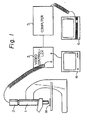
- Figure 1 shows a schematic diagram of an automatic etch pits counting system.
- an ITV camera 2 which outputs video signals representing an enlarged image of the surface of wafer W, the signals being processed by a computer 5.
- the reference numeral 3 denotes a video controller
- 4 denotes a monitor television
- 6 denotes a console for applying operating instructions to the computer, which has a display for displaying information such as input instructions and counting results.
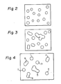
- the enlarged images of the surface of the wafer W will present various states. Depending on such states, the etch pits density may be low or high. If the etch pits density is high, a plurality of etch pits have tendency to overlap one another.
- Figures 2 and 3 show respective examples of the enlarge wafer images.
- Figure 2 shows one example in which only individually isolated etch pits exist and a single etch pit in the image is shown as a circle.
- the number of etch pits can be automatically counted on the basis of the video signals outputted from the ITV camera 2 and the counted value directly equals the number of etch pits.
- FIG. 3 is an enlarged diagram showing a wafer having overlapping etch pits. If a plurality of etch pits overlap each other, there is no simple form. Furthermore, the number of overlapping etch pits is indefinite. For example, if two etch pits overlap each other, they appear in the form of dumbbells, and if a number of etch pits overlap each other then a form like a shapeless cloud is presented.
- the average area A of an isolated etch pit is predetermined, the area S of the image of a grouping of etch pits is measured and then the area S is arithmetically divided by the average unit area A to estimate the number of etch pits in the image.
- the number of etch pits n is estimated to obtain the total number of etch pits in that field.
- the etch-pit images in the visual field are 1,2,..., m and the areas thereof are Si,S 2 ,...,Sm, respectively, the number of etch pits n; in the i-th etch-pits image is given by and the total number of etch pits N is given by or where the average unit area A is common to all points on a wafer.
- the area A is assumed to present a fixed value for every wafer.
- the representation [x] means that fractions of .5 and over are counted as a unit and that the rest are disregarded in connection with the value of x.
- the automatic etch pits counting method of the above system has utilized only one average unit area A, in spite of the variation of the measured points thereon.
- the average unit area A is calculated and decided for every wafer, or at every relatively fractionalized measured point thereon.
- a method of counting the number of etch pits in a semiconductor single crystal wafer comprising enlarging the surface image of the crystal wafer with a microscope, converting the image to corresponding digital data, and analysing the digital data to determine the density of etch pits over the area of the wafer, characterised in that the enlarged image is converted to video signals by a TV camera and the step of analysing the digital data comprises processing the image of the etch pits from the TV camera in a computer to obtain the area of individual etch pits, calculating the average unit area of the isolated etch pits for every wafer or at every measured point thereof, dividing the area of a group of overlapping etch pits by the average unit area, rounding off the resulting quotient to be an integer thereby obtaining the number of etch pits in the area, and automatically determining the total number of etch pits by totalling the number of isolated etch pits and the number of overlapping etch pits.
- the etch pits on a semiconductor wafer are automatically counted and, therefore, the operation for measuring is very fast and precise. Also, the operator is little tired and the number of operators can be reduced.
- the operator counts the etch pits by his own eyes through a microscope, he would count them at 10 points per wafer at least.
- it is easy to calculate the EPD at 50-100 points of measurement per wafer. Because of the increase of operating efficiency, the number of measured points can be increased and the quality of the semiconductor wafer can be strictly monitored.
- the average unit area Ap of the isolated etch pit is obtained for every wafer or at every measured point thereon, precise results of counting, or counting with little error, can be achieved, in comparison with the prior art which uses the average unit area A of a fixed value.
- the average unit area A of an etch pit varies for every wafer or at every measured point thereon and, therefore, such area is defined by suffixing "p", that is, Ap.
- the suffix "p" is an index given for every wafer or every measured point.
- the wafer W is placed on the sample base of the microscope 1.
- the enlarged image of the wafer is image-processed and converted to electrical signals by the ITV camera 2. While viewing monitor TV 4, the counting operation is automatically perfomed by the computer 5.
- the following method can be effected by the computer 5 and the instructions from the console 6 thereto and the operator, therefore, does not need to view the image with his own eyes nor to perceive it using his brain.
- Step (1) is to give numbers 1, 2 ..., m to the respective etch pits and obtain the corresponding areas Si, S 2 , ..., Sm.
- a two-dimensional image which comprises the etch pits and the background thereof, is processed as a binary image in the form of black and white which, for example, corresponds to the etch pits and the background, respectively. Then, the image is divided into a grouping of microscopic cells in the form of a matrix configuration.
- the area of the cell is a fraction of the area of the etch pit and is extremely small.
- the area S; of the etch pit i is estimated by counting the number of cells which fill that each pit.
- the method of obtaining such area is publicly known.
- step (2) discrimination between isolated etch pits and the groupings of etch pits can be accomplished by the following:
- an average value of the area of an isolated etch pit is obtained and this value is considered as an average unit area Ap at that measured point. Assuming that the number of isolated etch pits is u, wherein (i) means the sum in relation to the isolated etch pit. This comprises step (3).
- Step (4) is to divide the area S k of the image of the overlapping etch pits by the average unit area Ap and to obtain the number of etch pits n k included in the area S k , or where the representationtinct means that, in connection with values in the bracket, fractions of .5 and over are counted as a unit and the rest are disregarded.
- Step (5) is to obtain the total number of etch pits N, or where the representation of a first term means the sum on the isolated etch pit and means the sum on the grouping of etch pits.
- Fig. 4 is a sample of a microscopic image at a certain measured point on the wafer surface. Although the number of etch pits is relatively large in fact, for the sake of simplicity, a small number of etch pits are shown.
- Table I represents the data after step (1).
- the area corresponding to each of the etch pits is put in the associated column, as a multiple number of an area of any unit.
- the areas of Etch Pit Nos. 1, 2, 3, ... are given as 6, 8, 4, ..., respectively.
- step (1) is completed.
- step (2) isolated etch pits are distinguished from the groupings of etch pits. It is assumed that, by means of the steps as described above, each of Etch Pit Nos. 1, 3, 4, 7 has been perceived as an isolated etch pit. In the case of an isolated etch pit, the numeral "1" is put in the corresponding column of "Number of Etch Pits" of the table. In the case of a grouping of etch pit, the corresponding column of "Number of Etch Pits" remains vacant. This is shown by Table II.
- Step (3) is to obtain the average unit area Ap of each isolated etch pit.
- Etch Pit Nos. 1, 3, 4 and 7 are the isolated etch pits, respectively, and the areas corresponding thereto are 6, 4, 4, and 5, and therefore
- the area S k of the grouping of etch pits k is divided by Ap and then the quotient is rounded off to be an integer which is considered as the number of etch pits n k .
- the area of Etch Pit No. 5 is 19, and the value obtained by dividing it by Ap and rounding off is 4.
- the value of n k is put in the column of "Number of Etch Pits" corresponding to the grouping of etch pits. This is shown in Table III.
- Etch Pit Nos. 1 through 8 are perceived as 1, 2, 1, 1, 4, 2, 1 and 2.
- the etch pits density can be obtained by dividing the total number by the area of the wafer surface within the scope of the visual field.
- the present invention can be used to measure the etch pits density on the wafer surface of a semiconductor.
- the semiconductor wafers can be formed by slicing the ingots of single crystal such as GaAs InP, Si and Ge.
- the present invention may be applied to a general system for measuring the number of particles in a continuous member.
Landscapes
- Physics & Mathematics (AREA)
- Engineering & Computer Science (AREA)
- General Physics & Mathematics (AREA)
- Theoretical Computer Science (AREA)
- Chemical & Material Sciences (AREA)
- Health & Medical Sciences (AREA)
- Computer Vision & Pattern Recognition (AREA)
- Dispersion Chemistry (AREA)
- Geometry (AREA)
- Life Sciences & Earth Sciences (AREA)
- Analytical Chemistry (AREA)
- Biochemistry (AREA)
- General Health & Medical Sciences (AREA)
- Immunology (AREA)
- Pathology (AREA)
- Testing Or Measuring Of Semiconductors Or The Like (AREA)
- Length Measuring Devices By Optical Means (AREA)
Claims (1)
dadurch gekennzeichnet,
daß das vergrößerte Bild von einer Fernsehkamera (2) in Videosignale umgewandelt wird und die Auswertung der digitalen Daten die Verarbeitung des von der Fernsehkamera (2) erhaltenen Bildes der Ätzgrübchen in einem Computer zum Erfassen der Fläche der einzelnen Ätzgrübchen, das Errechnen der durchschnittlichen Flächeneinheit Ap der einzelnen Ätzgrübchen für jeden Wafer oder für jeden Meßpunkt eines Wafers, das Dividieren der Fläche Sk einer Gruppe von einander überschneidenden Ätzgrübchen k durch die durchschnittliche Flächeneinheit Ap, das Abrunden des resultierenden Quotienten zu einer ganzen Zahl, womit die Anzahl der Ätzgrübchen nk auf der Fläche Sk erhalten wird, und das automatische Bestimmen der Gesamtzahl N der Ätzgrübchen durch Zusammenzählen der Anzahl der einzelnen Ätzgrübchen u und der Anzahl der einander überschneidenden Ätzgrübchen Nk umfaßt.
Applications Claiming Priority (2)
| Application Number | Priority Date | Filing Date | Title |
|---|---|---|---|
| JP135308/83 | 1983-07-25 | ||
| JP58135308A JPS6027137A (ja) | 1983-07-25 | 1983-07-25 | 自動エツチピツト計数方式 |
Publications (3)
| Publication Number | Publication Date |
|---|---|
| EP0149685A1 EP0149685A1 (de) | 1985-07-31 |
| EP0149685A4 EP0149685A4 (de) | 1988-04-27 |
| EP0149685B1 true EP0149685B1 (de) | 1991-05-08 |
Family
ID=15148683
Family Applications (1)
| Application Number | Title | Priority Date | Filing Date |
|---|---|---|---|
| EP84902938A Expired - Lifetime EP0149685B1 (de) | 1983-07-25 | 1984-07-25 | Verfahren zum selbsttätigen zählen geätzter löcher |
Country Status (4)
| Country | Link |
|---|---|
| EP (1) | EP0149685B1 (de) |
| JP (1) | JPS6027137A (de) |
| DE (1) | DE3484563D1 (de) |
| WO (1) | WO1985000696A1 (de) |
Families Citing this family (4)
| Publication number | Priority date | Publication date | Assignee | Title |
|---|---|---|---|---|
| EP0486542B1 (de) * | 1989-08-10 | 1999-03-31 | International Remote Imaging Systems, Inc. | Verfahren zur differenzierung von partikeln basierend auf einer dynamisch änderlichen schwelle |
| ATE214024T1 (de) | 1997-12-18 | 2002-03-15 | Karl Keller | Lebensmittelverpackung und garverfahren für lebensmittel |
| US7027637B2 (en) * | 2002-02-21 | 2006-04-11 | Siemens Corporate Research, Inc. | Adaptive threshold determination for ball grid array component modeling |
| CN116577341B (zh) * | 2023-07-07 | 2023-09-19 | 深圳优普莱等离子体技术有限公司 | 一种金刚石表面刻蚀坑的合格检测方法及相关设备 |
Family Cites Families (5)
| Publication number | Priority date | Publication date | Assignee | Title |
|---|---|---|---|---|
| US3214574A (en) * | 1952-07-16 | 1965-10-26 | Perkin Elmer Corp | Apparatus for counting bi-nucleate lymphocytes in blood |
| DE1498814A1 (de) * | 1963-09-16 | 1969-04-30 | Halbleiterwerk Frankfurt Oder | Verfahren zur Bestimmung der Guete der Struktur von Einkristallen durch lichtoptische Registrierung |
| US3824393A (en) * | 1971-08-25 | 1974-07-16 | American Express Invest | System for differential particle counting |
| US4045655A (en) * | 1973-10-15 | 1977-08-30 | Hitachi, Ltd. | Automatic cyto-screening device |
| JPS5757246A (en) * | 1980-09-25 | 1982-04-06 | Fuji Photo Film Co Ltd | Detecting and measuring apparatus for flaw |
-
1983
- 1983-07-25 JP JP58135308A patent/JPS6027137A/ja active Pending
-
1984
- 1984-07-25 EP EP84902938A patent/EP0149685B1/de not_active Expired - Lifetime
- 1984-07-25 WO PCT/JP1984/000376 patent/WO1985000696A1/ja not_active Ceased
- 1984-07-25 DE DE8484902938T patent/DE3484563D1/de not_active Expired - Lifetime
Also Published As
| Publication number | Publication date |
|---|---|
| EP0149685A1 (de) | 1985-07-31 |
| WO1985000696A1 (fr) | 1985-02-14 |
| EP0149685A4 (de) | 1988-04-27 |
| JPS6027137A (ja) | 1985-02-12 |
| DE3484563D1 (de) | 1991-06-13 |
Similar Documents
| Publication | Publication Date | Title |
|---|---|---|
| US5012524A (en) | Automatic inspection method | |
| US6683974B1 (en) | Image defect detection apparatus and image defect detection method | |
| US7113628B1 (en) | Defect image classifying method and apparatus and a semiconductor device manufacturing process based on the method and apparatus | |
| TW388949B (en) | Quality management system and recording medium | |
| EP0663094B1 (de) | Verfahren und gerät zur identifizierung eines objekts mittels eine geordneten folge von grenz-pixel-parametern | |
| EP0149685B1 (de) | Verfahren zum selbsttätigen zählen geätzter löcher | |
| JPH044525B2 (de) | ||
| EP0272853A2 (de) | Verfahren und Einrichtung zum automatischen Lesen von Vernier-Mustern | |
| CN112991259A (zh) | 一种半导体制程缺陷的检测方法及系统 | |
| CA1217573A (en) | Automatic etch-pit counting system | |
| US20230206423A1 (en) | Method, apparatus, electronic device, and storage medium for determining defect shape of wafer | |
| DE69905605T2 (de) | Verfahren zur messung der grösse von polykristallinenbruchstückeund ihrer verteilung beim zufuhr in einem czochralski verfahren | |
| JP2001345357A (ja) | 半導体ウェーハの測定方法、半導体ウェーハの製造方法及び半導体ウェーハの測定装置 | |
| JP3705358B2 (ja) | 化合物半導体ウェーハにおける転位ピット密度の測定方法 | |
| KR102638903B1 (ko) | 연마 공구의 표면 미세 연마 입자 비전 분석 장치 및 방법 | |
| JP2002228596A (ja) | 半導体ウェーハの測定方法及び半導体ウェーハの製造方法 | |
| CN113393513B (zh) | 电影银幕穿孔测量方法、测量装置及计算设备 | |
| JPH04156212A (ja) | 架空線の自動点検方法 | |
| JP4061760B2 (ja) | 粒子画像領域分割方法 | |
| JP3745075B2 (ja) | 膜厚測定装置 | |
| JPH0671039B2 (ja) | ダイボンディング状態の検査装置 | |
| CN115205288A (zh) | 工业缺陷检测方法和装置 | |
| JPH07118100A (ja) | 半導体単結晶エッチピット密度測定方法 | |
| JPH0443311B2 (de) | ||
| JPH0682724B2 (ja) | ウエハ欠陥検査装置 |
Legal Events
| Date | Code | Title | Description |
|---|---|---|---|
| PUAI | Public reference made under article 153(3) epc to a published international application that has entered the european phase |
Free format text: ORIGINAL CODE: 0009012 |
|
| 17P | Request for examination filed |
Effective date: 19841122 |
|
| AK | Designated contracting states |
Designated state(s): DE FR GB |
|
| A4 | Supplementary search report drawn up and despatched |
Effective date: 19880427 |
|
| 17Q | First examination report despatched |
Effective date: 19900305 |
|
| GRAA | (expected) grant |
Free format text: ORIGINAL CODE: 0009210 |
|
| AK | Designated contracting states |
Kind code of ref document: B1 Designated state(s): DE FR GB |
|
| REF | Corresponds to: |
Ref document number: 3484563 Country of ref document: DE Date of ref document: 19910613 |
|
| ET | Fr: translation filed | ||
| PLBE | No opposition filed within time limit |
Free format text: ORIGINAL CODE: 0009261 |
|
| STAA | Information on the status of an ep patent application or granted ep patent |
Free format text: STATUS: NO OPPOSITION FILED WITHIN TIME LIMIT |
|
| 26N | No opposition filed | ||
| PGFP | Annual fee paid to national office [announced via postgrant information from national office to epo] |
Ref country code: FR Payment date: 19960709 Year of fee payment: 13 |
|
| PGFP | Annual fee paid to national office [announced via postgrant information from national office to epo] |
Ref country code: GB Payment date: 19960716 Year of fee payment: 13 |
|
| PGFP | Annual fee paid to national office [announced via postgrant information from national office to epo] |
Ref country code: DE Payment date: 19960802 Year of fee payment: 13 |
|
| PG25 | Lapsed in a contracting state [announced via postgrant information from national office to epo] |
Ref country code: GB Free format text: LAPSE BECAUSE OF NON-PAYMENT OF DUE FEES Effective date: 19970725 |
|
| GBPC | Gb: european patent ceased through non-payment of renewal fee |
Effective date: 19970725 |
|
| PG25 | Lapsed in a contracting state [announced via postgrant information from national office to epo] |
Ref country code: FR Free format text: LAPSE BECAUSE OF NON-PAYMENT OF DUE FEES Effective date: 19980331 |
|
| PG25 | Lapsed in a contracting state [announced via postgrant information from national office to epo] |
Ref country code: DE Free format text: LAPSE BECAUSE OF NON-PAYMENT OF DUE FEES Effective date: 19980401 |
|
| REG | Reference to a national code |
Ref country code: FR Ref legal event code: ST |