EP0148488B1 - Semiconductor memory having multiple level storage structure - Google Patents
Semiconductor memory having multiple level storage structure Download PDFInfo
- Publication number
- EP0148488B1 EP0148488B1 EP84116060A EP84116060A EP0148488B1 EP 0148488 B1 EP0148488 B1 EP 0148488B1 EP 84116060 A EP84116060 A EP 84116060A EP 84116060 A EP84116060 A EP 84116060A EP 0148488 B1 EP0148488 B1 EP 0148488B1
- Authority
- EP
- European Patent Office
- Prior art keywords
- data
- gate
- cells
- semiconductor memory
- memory
- Prior art date
- Legal status (The legal status is an assumption and is not a legal conclusion. Google has not performed a legal analysis and makes no representation as to the accuracy of the status listed.)
- Expired - Lifetime
Links
Images


Classifications
-
- G—PHYSICS
- G11—INFORMATION STORAGE
- G11C—STATIC STORES
- G11C11/00—Digital stores characterised by the use of particular electric or magnetic storage elements; Storage elements therefor
- G11C11/21—Digital stores characterised by the use of particular electric or magnetic storage elements; Storage elements therefor using electric elements
- G11C11/34—Digital stores characterised by the use of particular electric or magnetic storage elements; Storage elements therefor using electric elements using semiconductor devices
- G11C11/40—Digital stores characterised by the use of particular electric or magnetic storage elements; Storage elements therefor using electric elements using semiconductor devices using transistors
-
- G—PHYSICS
- G11—INFORMATION STORAGE
- G11C—STATIC STORES
- G11C11/00—Digital stores characterised by the use of particular electric or magnetic storage elements; Storage elements therefor
- G11C11/56—Digital stores characterised by the use of particular electric or magnetic storage elements; Storage elements therefor using storage elements with more than two stable states represented by steps, e.g. of voltage, current, phase, frequency
- G11C11/565—Digital stores characterised by the use of particular electric or magnetic storage elements; Storage elements therefor using storage elements with more than two stable states represented by steps, e.g. of voltage, current, phase, frequency using capacitive charge storage elements
-
- G—PHYSICS
- G11—INFORMATION STORAGE
- G11C—STATIC STORES
- G11C11/00—Digital stores characterised by the use of particular electric or magnetic storage elements; Storage elements therefor
- G11C11/21—Digital stores characterised by the use of particular electric or magnetic storage elements; Storage elements therefor using electric elements
- G11C11/34—Digital stores characterised by the use of particular electric or magnetic storage elements; Storage elements therefor using electric elements using semiconductor devices
- G11C11/40—Digital stores characterised by the use of particular electric or magnetic storage elements; Storage elements therefor using electric elements using semiconductor devices using transistors
- G11C11/401—Digital stores characterised by the use of particular electric or magnetic storage elements; Storage elements therefor using electric elements using semiconductor devices using transistors forming cells needing refreshing or charge regeneration, i.e. dynamic cells
- G11C11/4063—Auxiliary circuits, e.g. for addressing, decoding, driving, writing, sensing or timing
- G11C11/407—Auxiliary circuits, e.g. for addressing, decoding, driving, writing, sensing or timing for memory cells of the field-effect type
- G11C11/409—Read-write [R-W] circuits
- G11C11/4091—Sense or sense/refresh amplifiers, or associated sense circuitry, e.g. for coupled bit-line precharging, equalising or isolating
-
- G—PHYSICS
- G11—INFORMATION STORAGE
- G11C—STATIC STORES
- G11C7/00—Arrangements for writing information into, or reading information out from, a digital store
- G11C7/06—Sense amplifiers; Associated circuits, e.g. timing or triggering circuits
- G11C7/065—Differential amplifiers of latching type
-
- G—PHYSICS
- G06—COMPUTING; CALCULATING OR COUNTING
- G06F—ELECTRIC DIGITAL DATA PROCESSING
- G06F11/00—Error detection; Error correction; Monitoring
- G06F11/07—Responding to the occurrence of a fault, e.g. fault tolerance
- G06F11/08—Error detection or correction by redundancy in data representation, e.g. by using checking codes
- G06F11/10—Adding special bits or symbols to the coded information, e.g. parity check, casting out 9's or 11's
- G06F11/1008—Adding special bits or symbols to the coded information, e.g. parity check, casting out 9's or 11's in individual solid state devices
- G06F11/1072—Adding special bits or symbols to the coded information, e.g. parity check, casting out 9's or 11's in individual solid state devices in multilevel memories
-
- G—PHYSICS
- G11—INFORMATION STORAGE
- G11C—STATIC STORES
- G11C29/00—Checking stores for correct operation ; Subsequent repair; Testing stores during standby or offline operation
-
- G—PHYSICS
- G11—INFORMATION STORAGE
- G11C—STATIC STORES
- G11C7/00—Arrangements for writing information into, or reading information out from, a digital store
- G11C7/06—Sense amplifiers; Associated circuits, e.g. timing or triggering circuits
Definitions
- the present invention relates to a semiconductor memory and particularly to a semiconductor multilevel memory having multiple storage levels of information per memory unit even under a low power supply voltage and cnsumes less electrical power.
- a semiconductor memory having a higher integration density represented by a dynamic random access memory (hereinafter abbreviated as DRAM), has been developed year after year and a memory unit of semiconductor memory (hereinafter referred to as memory cell) and peripheral circuits are more and more superminiaturized.
- DRAM dynamic random access memory
- memory cell memory unit of semiconductor memory
- improvement in integration density by such superminiaturization must usually be accompanied by a large stride of advancement of element process technology such as photorithogrphy and etching, etc. and therefore a certain period is usually requried for devlopment of element process technology.
- an existing semiconductor memory is said not only as it is insufficient from the point of view of integration density but also in sufficient from the point of view of power consumption and other performances.
- a memory having multiple level storage structure is considered as an effective means for realizing a semiconductor memory having a higher integration density by the current process technology.
- This memory is intended to substantially increase integration density by causing a single memory cell to store the data of more than two (2) levels.
- CTD charge transfer device
- the MLS memory using CTD is not yet often put into practical use, because a number of levels cannot be increased so much in order to prevent that a multilevel data of analog signal is substantially attenuated due to finite transfer efficiency peculiar to the CTD.
- such multilevel memory is inferior in such a point that it is necessary to raise a driving pulse voltage in order to increase the transfer efficiency and such element intrinsically has a high capacitance load and consumes a very high electrical power.
- a MLS memory is also disclosed in FR-A-2 246 022.
- the read circuit described in this document is only reliable if the storage capacitor is considerably larger than the capacity of the data lines and the input capacity of the read circuit.
- EP-A-0 139 196 a charge transfer amplifier is described which amplifies the signal voltages on the data line with high accuracy.
- EP-A-0 130 614 discloses a MLS memory in which a multi-level step voltage is applied to the plate electrode of the storage capacitor or to the gate electrode of the associated MOS-FET of the memory matrix for reading and writing data of more than two voltage levels from or into the capacitor.
- DRAM dynamic memory
- a dynamic memory (DRAM) for addressing by both rows and columns is caused to store the multiple level data as an MLS memory for eliminating various disadvantages of an MLS memory using CTD described above and the A/D, D/A converters are also provided in the sensing and writing sytems.
- DRAM dynamic memory
- a very difficult problem explained below must be solved in order to use such DRAM as an MLS memory.
- a MLS memory can be used as an excellent large capacity memory when a number of memory cells which is equal to or larger than that of an ordinary 2-level memory are mounted on a chip in such a size as is equal to or smaller than that of said 2-level memory.
- current signal charge of one memory cell of DRAM is Q s '
- a signal charge allowed for one level of multilevel memory becomes about Q s '/N when a number of level is N. It is a very severe condition.
- an amplifier which can amplify a minute signal with high accuracy and a small size A/D converter with high accuracy are simultaneously required for an MLS memory for addressing both rows and columns. But such amplifier and converter cannot be realized and accordingly an MLS memory of this type cannot be developed.
- MLS memory multiple level storage structure
- the present invention provides an MLS memory comprising a newly developed minute voltage amplifier which is just suited to a large capacity memory, a highly accurate A/D, D/A converting structure even with simplified configuration and low power consumption and peripheral circuit with less power consumption.
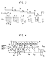
- Fig. 1 is a block diagram of an embodiment of the present invention.
- Fig. 2 is a schematic diagram for explaining the A/D conversion during the read operation by an MLS memory as the embodiment of the present invention.
- Fig. 3 is a schematic diagram for explaining the D/A conversion during the read operation by an MLS memory as the embodiment of the present invention.
- Fig. 4 is a circuit diagram of an embodiment of colum register of the present invention.
- Fig. 5 shows pulse timing of the embodiment shown in Fig. 4 of the present invention.
- Fig. 6 is a sectional view of an embodiment of the BCT amplifier.
- Fig. 7 shows the timings (A) and potentials (B-1 5) of pulses for driving the amplifier of Fig.6.
- Fig. 1 is a block diagram of an embodiment of the present invention.
- Fig. 2 is a schematic diagram for explaining the A/D conversion during the read operation by an MLS memory as the embodiment of the present invention.
- Fig. 3 is a schematic diagram for
- FIG. 8 shows the timings (A) and potentials (B-1 to B-6) of the same pulses.
- Fig. 9, Fig. 10, Fig. 25 show sectional views of other embodiments of BCT amplifier.
- Fig. 11 shows an embodiment of the signal sense circuit of the present invention.
- Fig. 12 shows drive pulses and internal waveforms used in Fig. 11.
- Fig. 13 shows a circuit diagram of sense amplifier by another embodiment of the present invention.
- Fig. 14 shows drive pulses and internal waveforms used in Fig. 13.
- Fig. 15 shows a circuit diagram of sense amplifier by the other embodiment of the present invention.
- Fig. 16 shows drive pulses and internal waveforms used in Fig. 15.
- Fig. 17 shows operation waveforms of the present invention.
- FIG. 19 show circuit diagrams of decoder and encoder by the embodiment of the present invention.
- Fig. 20 shows timings of drive pulses used for the encoder shown in Fig. 19.
- Fig. 21 shows a circuit diagram of triggering pulse generator by an embodiment of the present invention.
- Fig. 22 shows internal waveforms in Fig. 21.
- Fig. 23 shows another embodiment of the present invention.
- Fig. 24 shows drive pulses used in Fig. 23.
- Fig. 26 shows a circuit diagram of another embodiment of the present invention.
- Fig. 27 shows a structure of column register indicating an embodiment of the present invention.
- Fig. 28, Fig. 29 and Fig. 30 respectively show operation time charts in Fig. 27.
- Fig. 31 shows a structure of column register indicating another embodiment of the present invention.
- Fig. 20 shows timings of drive pulses used for the encoder shown in Fig. 19.
- Fig. 21 shows a circuit diagram of triggering pulse generator by an embodiment of the present invention
- FIG. 32 shows time charts of the circuit shown in Fig. 31.
- Fig. 34, Fig. 37 respectively show structures of colulmn registers indicating other embodiments of the present invention.
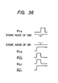
- Fig. 33, Fig. 35 and Fig. 36 show operation time charts.
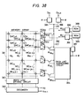
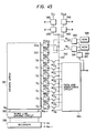
- Fig. 38, Fig. 43, Fig. 45 show structures indicating embodiments of semiconductor memories comprising a fault tolerate circuit by the present invention.
- Fig. 39 and Fig. 46 show circuit diagrams of data line addressing circuit used in said memory.
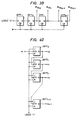
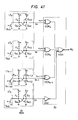
- Fig. 40, Fig. 47 show a counter circuit used in said memory.
- Fig. 41 shows a circuit diagram of ROM and comparator used in said memory.
- Fig. 42 shows a circuit diagram of switch circuit used in said memory.
- Fig. 44 shows a circuit diagram of comparator used in said memory.
- the present invention is explained by referring to the preferred embodiment thereof.
- data is carried and stored by the operations of electrons used as signal charge carriers but the holes can also be used in the same way by changing the polarity of power supply and pulses and the conductivity type of semiconductors.
- Fig. 1 shows a block diagram of an embodiment of an MLS memory by the present invention.
- numeral 1 is unit cell (hereinafter referred to as memory cell) of memory.
- 2 is storage capacitor.
- 3 is switching transistor (switching MOS transistor) which operates as word gate.
- 4 is electrode of storage capacitor 2 which is usually connected to a DC power supply (V cc ) and earth (V so ).
- 5 is word line.
- 6 is data line.
- 7 is block of memory cell array.
- 11 is unit of dummy cell.
- 12 is dummy storage capacitor which is selected to 1/2 of information storage capacitor C s .
- 13 is switching MOS transistor which operates as dummy cell selection gate.
- 14 is electrode of dummy storage capacitor which is used in common as the electrode of storage capacitor of memory cell.
- a 15 is word line of dummy cell.
- 17 is block of dummy cell array.
- 18 and 19 are reset gate and reset gate line of dummy cell.
- 30 is reset gate of data line.
- 31 is write gate.
- 21 is array block of 30 and 31.
- the write gate among various gates is composed of a p-channel MOS transistor, while the others are composed of an n-channel MOS transistor.
- the p-channel MOS transistor is indicated by giving an arrow mark to the source thereof and the n-channel MOS transistor is indicated only by 32 is bias charge transfer amplifier (hereinafter referred to as BCT amplifier) which amplifies with high accuracy the signal voltages on the data line which has been divided into multilevel low voltages up to large voltages.
- 22 is block of array. 33 is sense amplifier.
- 23 is array block thereof.
- 34 is column register (temporary storage cell).
- 24 is array block thereof.
- 35 is a triggering pulse generator.
- 36 is multiple-level step voltage generator.
- 37 is control circuit which controls the sense systems 21, 22, 23.
- 38 is control circuit (shift register) for sending timing pulses to the column registers.
- 29 is row address select circuit.
- 25 is row address buffer.
- 26 is column address select circuit.
- A/D, D/A conversion means is realized a multiple-level step voltage generator 36 and a shift register 38 which are controlled by a triggering pulse generator 35, a row address buffer 25 which transfers multiple-level step voltage to the word line 5, a memory cell 1, a reset gate 30, writing gate 31, a column register 34, an input-output circuit 27 and a decoder/encoder 28.
- a number of multiple levels is set to four levels (2 bits) but in actual it is possible to select more large number of levels.
- Fig. 2 shows a schematic diagram for explaining the A/D conversion means of multiple level memory of the present invention under the data reading operation.
- 41 is a stepping voltage pulse ( ⁇ w ) to be applied to the word line 5.
- V is the positive direction of voltage.
- 42 is electron potentiala EP of memory cell 1.
- 44 corresponds to a potential of storage capacitor 2, while 45 to that of word gate 3 and 46 to that of data line 5, respectively.
- the lower side indicates the positive direction.
- 47 is an electrode of storage capacitor 4 and 48 is a word gate 3.
- 43 is a column register of multiple level data and there are four cells corresponding to multiple levels.
- the second level "2" of charge storage states (“10" in the binary data) is stored in the storage capacitor.
- the multiple level data readout above is no longer analog data but the digital data.
- This digital data is sent to the encoder through the output lines (in this example, used as the input-output common line (I/O line); refer to Fig. 4, Fig. 11, Fig. 18, Fig. 19) and is then read as the usually employed digital data such as binary code.
- I/O line input-output common line
- A/D conversion system is characterized in that after signal charge is output from memory cell, a charge packet only carries a binary digital data of ON and OFF, and multiple level data is effectively carried at the timings t1 ⁇ t5 which are given by the pulses sent from the triggering pulse generator which control the column register and the pulse ⁇ w applied to the word line.
- signal voltages on the data line does not require amplification of high precision analog value which is required for ordinary A/D conversion and can be processed as 2-level data for ordinary memory.
- the A/D conversion system of the present invention does not become a large scale and high power circuit which interferes realization of high integration density memory like the existing A/D conversion circuit and a memory with super-high integration density can be realized with less power consumption.
- Fig. 3 shows a schematic diagram indicating the D/A conversion means of MLS memory of the present invention under the writing operation.
- 51 is the stepping pulse ( ⁇ w ) to be applied to the word line 5.
- 52 is electron potential of memory cell 1, corresponding to the positions 44 ⁇ 46 and electrodes 47, 48 as in the case of Fig. 2.
- a data line is set to a low level (0V in this case) by the reset gate 30 (t6 ⁇ t7).
- the data line is raised to a high level through the write gate 31 when the pulse / w reaches the corresponding level (t8 ⁇ t9).
- the second level "2" is remained as indicated by 53 in the memory cell.
- the write pulse decodes the write data and is given to the write gate 31 through the write lead 39 at the dependent timing. Since the D/A conversion for writing is carried out also in this case at the timing (t7 ⁇ t11), the circuit structure is very simple, high integration density can be realized and power consumption is very low.
- the write-read means shown in Fig. 3 and Fig. 2 have such a large characteristic that the signal charges corresponding to a level does not almost change depending on the location when the level of pulse ⁇ w does not change in accordance with the position because the write and read operation to/from the data storage capacitor is carried through the same gate 3.
- a storage capacitor is C s
- a threshold voltage of gate 3 is V Ths
- a voltage of pulse ⁇ w in the writing operation is V W
- a voltage of pulse ⁇ w in the reading operation is V R
- a voltage V s of storage capacitor when data is written becomes V V W - V Ths
- Fig. 4 and Fig. 5 show respectively the practical example of circuit diagram of the column register, column address select gate (Y gate) and input-output circuit block 27 (herein after explained as a part of column register) in the embodiment shown in Fig. 1 and the pulse timing chart.
- 61 is a shift register corresponding to a control circuit which controls a storage 38 shown in Fig. 1. This register sends the pulse ⁇ SR shown in Fig. 5 to the column register.
- Fig. 5 shows the drive pules and internal waveforms in the READ/REFRESH mode of the MLS memory of the present invention.
- the data "2" is read and the same data is written again.
- the read gates 620 623 are precharged to a high level through the precharge gate 63 at the timing t0.
- the ascending stepping pulse is applied to the word line 5 (Fig. 1), signal charge is read to the data line 6 when the level is R2 (t3 ⁇ t4) and a voltage V0 drops (71).
- This signal is amplified by the voltage amplifier 32, judged by the sense amplifier 33 and appears on the output terminal 64 as an output voltage V so (72). This process is explained in detail later by referring to Fig.
- a voltage V D of data line 6 is reset to a low level (76) by the reset gate 30 at the timing t5.
- the descending stepping pulse is aplied to the word line 5 and the pulse ⁇ SR is sequentially applied as ⁇ W0 ⁇ W3 from the shift register 61 (t7 ⁇ t11).
- a MOS transistor 67 becomes conductive since a high level has been stored in the node 65 of gate 67 during the READ cycle and a voltage V RF of refresh line 68 becomes high level (77).
- V RF can be boosted up to a high level as in the case of ⁇ W2 without any influence of the threshold voltage, owing to the bootstrap effect by the capacitance 69 (including gate channel capacitance) between the gate and source.
- level "2" output to V RF as indicated as 77 also appears on the I/O line through the Y gate 70 if this column is selected by ⁇ YA .
- it is read as the 2-bit binary signal by sending it to the encoder to which the pulse being synchronized with ⁇ W3 ⁇ W0 is supplied.
- an output V RF 77 gives an inverted output (low level) to the writing gate 31 (Fig. 1) consisting of the p-channel MOS transistor by means of an inverter 59.
- a voltage V0 of data line is raised up to high level (78) and the level W2 is stored in the memory cell as shown in Fig. 3 (53). Namely, this operation is called REFRESH operation.
- the write enable signal ⁇ WE (Fig. 4) is set to low level and writing is not carried out externally. If it is required to write data externally, the signal ⁇ WE is set to high level and the signal V LG is set to low level, thereby the function of column register is disabled, the multiple level input signals obtaned by the decoder in the I/O line side are input in the timings ⁇ W3 ⁇ W0 and thereby the data can be written externally into the memory cell through the REFRESH line 68.
- a temporary storage (column register) providing N (or N-1) storage cells corresponding to a number of levels N has eliminated, when it is installed, a large scale circuit such as encoder, decoder and logic gate (exclusive OR gate and AND gate) required for refresh operation from each data line and is very important component which realizes the sense system of MLS memory with such an integration density as the DRAM in the maximum integration level.
- This storage has attained practically the high integration density MLS memory of the present invention for the first time.
- the precharge gate 63 among various gates uses the p-channel MOS transistor, while the other gates use the n-channel MOS transistors.
- the MLS memory As is already described, it is substantially important for the MLS memory for addressing by both rows and columns to amplify with high accuracy the signal per level which has been divided into minute signals of multiple levels.
- such requirement has been attained by providing a high performance bias charge transfer amplifier shown as 32 in Fig. 1 and an MLS memory which realizes a large number of multiple levels even at a low voltage has been embodied for the first time.
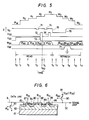
- Fig. 6 is a sectional view of BCT amplifier (bias charge transfer amplifier) which amplifies a minute signal of one level appearing on the data line up to such a voltage as can be sensed by the sense amplifier 33 consisting of the MOS transistor circuits.
- Fig. 7 shows drive pulse timings and potentials.
- Fig. 8 shows pulse timings and potentials indicating other driving method.
- Fig. 9 and Fig. 10 show the embodiments of BCT amplifier.
- 80 is an insulating film; 81 is an N type semiconductor substrate; 82 is a P-type well region; 83 86 are n+ layers; 87, 89 are charge transfer gates; 88 is a charge driving gate; 90 is a precharge gate; 92 is a sense amplifier input terminal.
- the reset gate 30 is set to the conductive state (ON state) by the reset pulse ⁇ R , resetting the data line 60 to 0V or a sufficiently low voltage.
- V T3H is a high level voltage of pulse applied to the gate 87
- V ThT3 is a threshold voltage (including substrate effect) of the gate 87.
- the gates 87 89 are then set to the OFF state and a bias charge stored under the drive gate 88 is also set (Fig. 7(B-2)).
- the signal charge carrier of storage capacitor 2 is read on the data line through the word gate 3 (93 of Fig. 7(B-2)). Then the gate 87 is set to ON state and the bias charge at the lower part of drive gate 88 is moved to the side of data line 6 (Fig. 7(B-3)).
- a capacitance (C D ) of data line 6 is considerably large among the node capacitances within the apparatus and often takes an order of PF. But, a capacitance of drive gate 88 is very small as compared with it. Therefore, the drive charge is mostly moved to the side of data line. At this time, a bias charge mixes with signal charges.
- the drive gate 88 is set to ON state and such mixed charges are fetched to the lower part of drive gate 88 (Fig. 7(B-4)). Moreover, the transfer gate 87 and drive gate 88 are set to OFF and charges are transferred to the input end side 92 of sense amplifier 92 (Fig. 7(B-5)). At this time, a voltage is is applied to the gates 87 ⁇ 89 in the same condition as (B-2) and the bias charge is not transferred and only the signal charge is transferred as 94 ⁇ 95.
- the drive pulse timing is shown in Fig. 7(A). Said bias charge transfer process is repeated for a number of times corresponding to a number of levels 9 (for example, 4 times in the case of four levels) for reading multiple level data reading. Namely, in the example of Fig. 2, the bias charge transferf is carried out once during the timing t1 ⁇ t2 and the timing t2 ⁇ t3 respectively. Such repetition may be allowed during the timing t23 ⁇ t28 as shown in Fig. 7(A) or may be allowed during the timing t21 ⁇ t28, except for the reset time of data line. Durting the latter timing, the bias charge under the drive gate 88 is reset in each timing and therefore when reading is conducted many times, the bias charge transfer can always be done with high accuracy by preventing that the charges are reduced by a tailing current of the gate T1 (89).
- the gate T3 (83) becomes cut-off state, a current usually does not almost flow under the gate T3 because a voltage amplitude is very small even when a minute signal appears on the data line as indicated by 93. It is because the gate T3 is in the tailing region at a very low level.
- the operating point of tailing rises and a current which is as large as different order flows and for example, charges of about 99% move to the lower side of gate T2.
- the signal charges of 99% are also included and when the bais charges are subtracted through the gate T1 (89), the signal charges can be moved to the sense amplifier input terminal 92 with a very good transfer efficiency.
- transfer of signal charges can be done for each gate under the saturated mode as indicated by (B-4), (B-5). If such transfer is carried out under non-saturated mode, transfer of signal charges is not conducted sufficiently due to the division of capacitance.
- Fig. 8 shows another driving method. This method is different from Fig. 7 in such a point that setting (B-3) of bias charge and transfer of such bias charge to the sense amplifier input terminal through the gate T1 (89) from the gate T2(88) are conducted under the condition that both T1 and T2 are ON. Thereby, the OFF level of each gate T1, T3 is simple cut-off state and it is not required to think of the conductive state of current. Thus, low level setting of pulse can be done easily (in many case, it can be set to 0V).
- Each reset of bias charge under the gate T2 described in Fig. 7 is carried out by setting the terminal 91 to low level in (B-2).
- the timing (t40) for making high level the pulse ⁇ T1 may be set to the timing t38 ⁇ t39 (B-5) where the pulses ⁇ T2 and ⁇ T3 are high level as shown by 96.
- Fig. 9 shows another embodiment of structure of BCT amplifier which is different from that of Fig. 6 in such a point that n ⁇ or n+ layer 101 is provided under the gate T2 (88).
- the gate T2 (88) As is apparent from the potential diagrams of Fig. 7, Fig. 8, it is better that the gate T2 (88) as the lowest threshold voltage V ThT2 among those of the gates T1(89) and T3(87) and it is the depletion type. If it is the depletion type, the drive pulse ⁇ T2 can be simplified as the maximum voltage (V cc ) of the 0V system.
- the gates T1 ⁇ T3 can be driven with the drive pulse of high level, low level and equal amplitude as is obvious from Fig. 7(B-1), Fig. 8(B-1) when there are relations, V ThT3 > V ThT1 > V ThT2 , V ThT2 ⁇ 0V, (V ThT1 ⁇ 0V).
- the gate T2 becomes only a simple capacitor, but as is apparent from operation principle of Fig. 7 and Fig. 8, the same effect as that obtained when the gate T2 is a MOS transistor can also be obtained.
- Fig. 10 is an embodiment where the tate T2 is considered as a capacitance (formed by the electrodes 102 and 103) on the field by considering it as only a simple capacitance. Thereby, the processing for providing the n ⁇ or n+ layer under the gate T2 is no longer necessary and the manufacturing process can be matched with that for ordinary memory LSI.
- the gate T2 is formed as the enhancement type, when the low level of drive pulse ⁇ T2 is set to 0V, recoupling of electron and hole pair occurs through the surface level at the semiconductor surface under the gate and charge transfer efficiency is deteriorated. But it can be prevented by setting low level of ⁇ T2 to a value higher than V Tht2 or by applying a negative bias to the well 82.
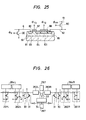
- Fig. 25 shows an embodiment indicating another structureof BCT amplifier which is different from the preceding embodiment in such a point that the gate T1 is eliminated.
- the bias charge under the gate T2 (88) is given by a voltage to be applied to the terminal 91 through the precharge gate.
- the pulse ⁇ T2 is set to low level, the bias charge is sent and it is set to high level again. Thereby, it is obtained together with the signal charage, as in the case of the preceding embodiment.
- the bias charge and signal charge are sent to the sense amplifier while these are mixed and these are judged. Since the input capacitance of sense amplifier becomes large, the amplification coefficient is not so large but structure can be simplified.
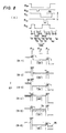
- Fig. 11 shows practical example of circuit structure of the signal sense system as a whole of the MLS memory of the present invention.
- Fig. 12 shows the drive pulse waveforms and internal waveforms.
- the elements given the same symbols such as 32, 33, 34, 27, 61, t3, t4, t31 ⁇ t41, etc. indicate the same elements and timings, etc.
- the timing waveforms shown in Fig. 12 indicate the condition that the data "2" is just stored in the memory cell and it is then extracted, considering the case where the cell connected to the data line 6 is selected ata the memory cell and a dummy data (in such an amount equal to 1/2 of signal charge) appears from the side of data line 6D.
- DP is a drive pulse
- IW is internal waveform.
- the data line voltage V D and data line voltage of dummy data V DD return to the original volates respectivelyu due to the bias charge transfer and the signal charge and dummy charge are respectively sent to the sense amplifier input terminals 92, 92D (t38 ⁇ t42).
- V SA , V SAD of sense amplifier input terminals 92, 92D are precharged to V D2 (it may be equal to V cc ) by the pulse ⁇ PP (t31 ⁇ t39) and when the gate T1 (89) becomes ON at the timing t40, voltage drop by said signal charge and dummy charge appears (112, 113; t40 ⁇ t42).
- the flip-flop type (hereinafter referred to as FF type) sense amplifier starts, a voltage V SA is dropped to low level (0V) and V SAD is also dropped (t42 ⁇ t43).
- V SA voltage
- V SAD voltage
- the P-channel MOS transistor Q FA2 becomes conductive, raising V SAD to V cc and the judging operation of sense amplifier is defined (t43 ⁇ t44). Since the pulse ⁇ FA2 makes conductive Q92, Q 92A , an output of the sense amplifier is sent to the column register.
- the pulses a1, a1 determine to which line of a pair of data lines 6 6D the signal charge and dummy charge are output.
- the pulse a1 is high level, while the pulse a1 is low level. Accordingly, V SAD defined to be high level raises a voltage V so of node 64 through the transistor Q 64D and thereby a voltage V LG of read gate 62 is also raised (t43 ⁇ t44). At this time, since the output ⁇ R2 of shift register is in the high level, a high level voltage is stored at the source end (65 of Fig. 4) of read gate as in the case of Fig. 4 and the multiple level data can be read. This data can be read to the external circuit, refreshed and written externally as explained with reference to Fig. 4 and Fig. 5.
- the FF type sense amplifier shown as 33 in Fig. 11 has the input dynamic range as wide as V cc to 0V and quickly amplifies the signal, owing to the positive feedback. As described later (Fig. 17), the signal appearing on 92, 92D easily has the offset due to the characteristic of BCT amplifier. Therefore, wide input dynamic range is just suited for the MLS memory of the present invention and accordingly more reliable operation of the sense system of MLS memory can be obtained.
- Fig. 13 shows a differential type high sensitivity amplifier as another embodiment of sense amplifier of the present invention.
- Fig. 14 shows drive pulse timings and internal waveforms.
- V SA , V SAD are precharged to high level (t31 ⁇ t35) through Q DA2 , Q DA2D (a1 is high level and a1 is low level).
- ⁇ T1 is set to high level and bias charge under the gate T2 is set at this time.
- the drain to gate of differential input transistors Q DI , Q DID becomes conductive. Therefore, offset by dispersion of threshold voltage between these transistors can be compensated and a very sensitive sense amplifier can be realized.
- the precharge level 141 of V SA , V SAD is a value which is different by only ⁇ V T .
- the timing t35 ⁇ t40 means the period where the bias charge transfer already described is carried out.
- ⁇ T1 becomes high level at the timing t40, the signal charge and dummy charge respectively appear on the 92 and 92D and these are judged by the sense amplifier.
- V SAD becomes higher than V SA (V SAD > V SA ) (142) and the node 131 is lowered to low level.
- the pulse a1 is low level, it is transferred to the gate 132 of transistor Q DA3 and the pulse ⁇ DA3 is raised to high level (t52). Thereby, the column register is started.
- V SAD becomes lower than V SA (V SAD ⁇ V SA ). Accordingly, the node 131 is high level and V SO remains at low level.
- the termial 133 is not connected to V cc and the pusle ⁇ DA3 is applied thereto because it must be prevented that the output V SO sometimes rises even when any data is not actually applied while pulse noise enters to each node due to ON-OFF of drive pulse and it is amplified up to such a degree as appearing at 132.
- This differential sense amplifier is capabale of reducing an input capacitance because only one gate of transistors Q DI and Q DID is respectively coupled to the input terminals 92, 92D and is easily raising the amplification coefficient of the BCT amplifier.
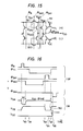
- Fig. 15 is another embodiment of sense amplifier used in the present invention.
- Fig. 16 shows the drive pulse (DP) timings and internal waveforms(IW).
- the sense amplifier shown in Fig. 15 is not differential type and the dummy charge is not used for judgement.
- V SA of 92 is lowered by the pulse ⁇ R (161)
- the pulse ⁇ SA2 is set to low level and V SA is precharged to V cc -
- V TP is a threshold voltage (V TP ⁇ 0V) of p-channel MOS transistor.
- ⁇ T1 is set to high level and thereby a bias charge under the gate T2 is set (t62 ⁇ t39).
- the timing t35 ⁇ t40 is the bias charge transfer period. When ⁇ T1 becomes high level at the timing t40, signal charge appears on 92.
- ⁇ SA1 is set to high level and voltage V SB of 151 is set to 0V (t63 ⁇ t64).
- V SA is set to V cc -
- An output can be obtained at V OS by sampling V SB with ⁇ SA4 (t65).
- the sense amplifier of Fig. 15 has the characteristic that it can be realized with comparatively less amount of transistors and is suited to high integration.
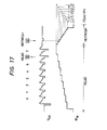
- Fig. 17 shows internal waveforms to be used for actual MLS memory operation of 8-level(3-bit)/cell in the embodiment of the present invention shown in Fig. 1.
- the lower stage indicates a voltage ⁇ W applied to the word line and the upper stage indicates a voltage (V SA ) at the point of 92 in Fig. 1. Namely, it is a voltage waveform at the bias charge transfer amplifier output terminal (sense amplifier input terminal).
- V SA voltage waveform at the bias charge transfer amplifier output terminal (sense amplifier input terminal).
- the data stored in the level "6" (“110" in the binary data) is read together with the ascending pulse and it is then written to the level "6" by the descending pulse.
- one step of ⁇ W means 200 mV and therefore one step of signal voltage of memory cell is about 200 mV.
- On the data line such voltage is about 15 mV and it is amplified by BCT amplifier up to about 10 times and thereby an output as high as 150mV can be obtained.
- V SA drops a little.
- the BCT amplifier is accompanied by various kinds of noise and it is more practical from the point of view of high accuracy to judge the signal with the sense amplifier which is used for comparing difference of dummy charges.
- the signal can be sensed more easily by comparing it with the dummy charge sent from the dummy cell.
- the address select circuits 24, 28 which are the same as those in the existing memory may be used.
- the multiple level data read to the storage node (65 etc.) of column register from the memory cell is read to the common input-output line (I/O line; Fig. 4) as the timing signal being synchronized with the pulses ( ⁇ W0 , ⁇ W1 , ...) sent from the shift register 61 and external data is also written by sending the timing signal corresponding to the multiple level from the I/O line in the same way.
- Fig. 18 and Fig. 19 respectively show the embodiments of decoder and encoder which have realized said input-output circuits.
- Fig. 20 shows the drive pulse timing chart of the encoder shown in Fig. 19.
- the node 191 is precharged to V cc by the pulse ⁇ P at the timing t70 ⁇ t71.
- ⁇ WE is high level, it is kept at V cc .
- the pulses ⁇ M3 , ⁇ M2 , .... are sequentially applied as shown in Fig. 20, prior to the pulses ⁇ W3 , ⁇ W2 , etc sent from the shift register. For example, in case the level "2" is read, the voltage V I/O of I/O line rises at the timing of ⁇ W2 (t72 ⁇ t73).
- Fig. 21 shows an embodiment of circuit structure of triggering pulse generator 35 invented in view of solving problems mentioned above and Fig. 22 shows internal waveforms.
- a pulse generator shown in Fig. 21 increases the oscillation frequency as much as an increase of heat generating current (hereinafter referred to as a leak current) due to a temperature rise and thereby the refresh period of memory cell can be shortened and destruction of multiple level data by leak current can be prevented.
- a leak current heat generating current
- a pulse generator 210 shown in Fig. 21 comprises a pseudo memory cell similar to memory cell.
- the leak current 211 and the inverter circuit connected thereto is started.
- V G1 is in the low level and V1 is precharged to high level. Thereafter, when it is set to high level (t80), a voltage V1 of node 212 is discharged by the leak current.
- V1 becomes lower than V cc -
- the transistor Q OS2 becomes conductive and the inverter is sequentially reversed.
- V s (V G1 ) is dropped to the low level and V1 is precharged again to the high level (t82).
- V14 becomes high level, giving an output (t83).
- V G1 V G1
- N N in Fig. 22 indicates a number of stages of inverters counted from the node 212.
- Fig. 23 shows another embodiment of the present invention and Fig. 24 shows the operation principle.
- the same symbols as those in Fig. 1 show the portions having the same function.
- the stepping waveform sent from the stepping pulse generator 231 is stored in the storage capacitor electrode (hereinafter called a plate) 232 ( ⁇ P2 ) of memory cell and as shown in Fig. 24, the descending stepping pulse is applied for reading operation while the ascending stepping pulse for writing operation, respectively.
- the pulse ⁇ WR applied to the word gate 233 is an ordinary binary pulse but its high level (ON state) is set to a voltage V WR1 ( ⁇ V cc ) which is a little higher than the threshold volage of word gate.
- the level "2" is stored, the bottom of electron potential of storage capacitor 24 sequentially ascends with sequential descending of ⁇ PL such as OFF - R0 - R1 - ..., the signal flows toward the data line at the timing of R2 (243), it is judged by the signal sensing systems 22, 23 and is then read through the column register 34.
- the data line voltage is set to a voltage which is a little higher than ⁇ WR - ⁇ ThN (V ThN is a word gate voltage) in place of 0V when / PL reaches the level of W2 (V D1 ⁇ V cc ) (t91).
- V ThN is a word gate voltage
- the embodiment shown in Fig. 23 and the driving method of Fig. 24 are characterized by that since it is not required to raise the data line to V cc from 0V at the time of writing opeation, power consumption due to the charging and discharging of data line during writing operation is small and rise of word gate voltage due to the coupling between the word line 233 and data line 6 can be kept very small.
- the plate is not used in common for all cells but it is separated for each cell by the word and accordingly cell array has a little larger area.
- the terminal 40 of writing gate 31 (Fig. 1) is not set to V cc but to the specified voltage V D1 (>/ WR (ON) - V ThN ) .
- the maximum charges Q s of one memory cell is set to almost equal to the charges Q s ' of DRAM of only the ordinary binary data in order to obtain practical merit of MLS memory, namely a high integration density. Therefore, the signal charge Q s/N per level divided into (N) multiple level is vary small and it is difficult to directly sense a voltage appearing on the data line 6 with the sense amplifier consisting of the MOS transistor. Such voltage can be sensed actually by the BCT amplifier of the present invention. On the contrary, it is very difficult from the point of view of integration density to provide the A/D, D/A converter of multiple level data after the BCT amplifier.
- the embodiments of the present invention described above employ the data line structure of folded bit line type as the memory structure shown in Fig. 1, Fig. 11 and Fig. 23.
- the present ivention can also be adapted to the data line structure of open bit line type as shown in Fig. 26.
- Fig. 26 shows an embodiment of the MLS memory of the present invention employing the open bit line type data line structure.
- the elements given the same numbers indicate the same elements.
- 261L, 261R are memory cells; 262L, 262R are dummy cell; 263L, 263R are bias charge transfer amplifier (BCT ampliier); 264L, 264R are row address select and buffer circuits; 267 is an input-output circuit array and column address select gate block.
- the signal is respectively amplified by the BCT amplifiers 263L, 263R and are judged by the sense amplifier 33. After the signal is temporarily held by the column register 34, the signal is read through the input-output circuit 267.
- the writing operation is also carried out as in the case of existing example.
- a memory having the general characteristic of this type namely a memory having the performance that a high speed operation can be realized because the word line can be formed by the metal such as aluminium can be obtained.
- the signal is mainly compared using a dummy cell as shown in Fig. 1, Fig. 11, Fig. 23 and Fig. 26.
- the present invention can be adapted to the system where the sense amplifier not using the dummy signal shown in Fig. 15 is used.
- the signal sent to the sense amplifier from the BCT amplifier often allows in each reading operation superposition of equivalent noise charges other than the signal charges due to the influence of pulse coupling or tailing current. In this case, the signal can be more easily and accurately judged using the signal (Q s /2N) sent from the dummy cell as is already explained regarding the internal waveforms of element shown in Fig. 17.
- the signal flows only in the one direction and therefore since the column address select gate and column register are opposingly located to the memory array for the sense amplifier, the consitution of the folded bit line type is simpler than tha tof open bit line type.
- the embodiment of the present invention described above is capable of further enhancing the effect thereof by the method, where the sense amplifier input terminals 92, 92D are divided, for example as shown in Fig. 11, by inserting a gate between the input terminal and BCT amplifier output terminal and thereby a coupling noise of pulse can be reduced.
- An embodiment of the present invention partly uses the CMOS (complementary MOS) circuit and it can be formed only with the N or P channel MOS transistor. However, if it is formed only with a single porality transistor, it is also followed by the general trend that power consumption increases.
- CMOS complementary MOS
- the driving method explained for the embodiment of the present invention is particularly considered for obtaining sufficient effect of the present invention but such method is not limited only to it and other method can also be adapted.
- the present invention provides an MLS memory for addressing by both rows and columns with a low power consumption comprising an amplifier which is just suited to a large capacity memory because of its simple structure and is capable of amplifying a minute voltage with a low voltage drive pulse and a high precision A/D, D/A conversion means which also has small scale circuit structure and can be driven with a low voltage in view of high integration density.
- a semiconductor file memory having an ultra-high integration density which is expected for a small size computer system can be realized.
- Such semiconductor file memory fantastically improves a small size sotrage unit using semiconductor, for example, an IC cards, etc.
- the column register (temporary storage circuit) used in the present invention executes AD/DA conversion between multiple level signal and digital information and plays a very important function for an MLS memory.
- reading is carried out serially in such a timing that the potential of input-output signal changes. Therefore, in the case of reading a multiple level data, for example, the data of 16 levels, the control signals ⁇ W0 ⁇ W15 must sequentially be set to "H" level for each column and a longer time is required.
- a device which is capable of quickly reading the data of multiple levels, if it is required to read the data from the column register of the MLS memory, is provided.
- a second group of storage cells is disposed corresponding to the group of memory cells in such a column register that the digital data corresponding to the timing of voltage change of input signal sent from the sense amplifier is written into the group of storage cells and the data stored in said groups of storage cells is read and it is then written into the memory cells.
- Fig. 27 shows the structure of another embodiment of the column register of the present invention. ( ⁇ R0 ⁇ R3 , ⁇ W0 ⁇ W3 are arranged reversely to Fig. 4)
- the second storage cell groups 280, 281 are provided in addition to the first storage cell groups 270 to 273 arranged previously.
- the data equivalent to that stored in the first storage cell groups is also stored in such second storage cell groups and the second storage cell groups 280, 281 which assure the high speed data reading are used for reading the data to the external circuits.
- the second storage cell groups 280, 281 have the same structure and therefore description about structure of storage cell 281 is omitted here. These storage cell groups are arranged in both upper and lower directions with a plurality of cells.
- the 3-MOS transistor type memory cell namely, in the case of cell 280, a memory cell using 3-MOS transistors 284, 285, 286, three lines D0, 282, 283 and the earth line is used.
- the transistor 284 is used for storing
- the transistor 285 is used for reading
- the line 282 is used as the write word line
- the line 283 is used as the read word line
- the line D0 is as the data line
- the point B is the storage node.
- a number of second storage cells can be determined by log2n for a number of levels n (n is a positive integer) of the MLS memory. It may be describ ed later, it is of course possible to set a number of second storage cells to a number of levels of MLS memory. From the view point of cost of the circuits to be used, it is obvious a less number of second storage cells results in a large economical merit.
- Fig. 28, Fig. 29, Fig. 30 respectively show the writing and reading operation time charts of the column register shown in Fig. 27.
- the digital data is written corresponding to the timing of the input signal ⁇ in (V SO of Fig. 4) to change to L level from H level.
- the switch 60 of Fig. 27 is turned ON and the switch 287 is connected to the side S1 indicated in the figure. Accordingly, the input signal ⁇ in is supplied to the first group of storage cells 270 273 and the second group of storage cells 281, 282 from the line 62 to the line 282.
- the input signal ⁇ in makes transition to L from H level at the 4 kinds of timings and therefore the digital data corresponding to these timings are written into the first and second groups of storage cells.
- explanation of the first group of storage cells is omitted because it is the same as that shown in Fig. 4 and only operations of second group of storage cells are explained.
- the control signals ⁇ D0 , ⁇ D1 synchronized with the timing of voltage change of input signal ⁇ in are respecitvely supplied to the group of control lines D0, D1 connected to the second group of storage cells.
- the control signals ⁇ D0 , ⁇ D1 change as shown in Fig.28 in accordance with the 2-bit binary code. Namely, first, both signals are "L”, then only ⁇ D0 turns to “H” , then only ⁇ D1 turns to "H” and finally both signals are "H".
- Fig. 30 Operations of externally writing the data to the first storage cell of the first column are explained by referring to Fig. 30.
- the switch 60 of Fig. 27 is turned OFF and the switch 287 is set to the side S2 opposing to the position indicated in the figure.
- the column select signal ⁇ YA is supplied to the first group of storage cells 270 273 through the lines 283 and 62.
- the data to be written is set to the control signals ⁇ R0 ⁇ R3 . At this time, only one must be “H” level and others must be “L” level. In Fig. 30, only the control signal ⁇ R1 is "H" level.
- Fig. 31 shows a constitution of column register indicating another embodiment of the present invention.
- This embodiment is different from that in Fig. 27 in the the internal structure of the first group of storage cells 270 ⁇ 273, wherein three MOS transisors are comprised.
- Fig. 32 shows the operation time chart of the circuit shown in Fig. 31.
- the line 62 connected to the output signal ⁇ out is precharged to the "H” level.
- the control signals ⁇ W3 ⁇ W0 are sequentially set to the "H” level.
- the control signals ⁇ W3 ⁇ W0 are supplied to the gate of MOS transistor 276 in the first group of storage cells 270 ⁇ 273 of each column through the control lines W 0 ⁇ W 3 , making the transistor 276 ON.
- the precharged line 275 is discharged through the transistors 276 and 275 and thereby this line is set to "L” level.
- the output signal ⁇ out becomes "L” level at the timing where the control signal ⁇ W2 becomes “H” level.
- the same MOS transistor 274 is used in common when the data corresponding to the timing of voltage change of input signal ⁇ in is written into the first group of storage cells 270 273 and when the data is externally written into the group of storge cells 270 273, but it if of course possible to used different MOS transistors.
- the driving method using the grey code has an advantage that a number of times of rising and falling of the control signals ⁇ D0 , ⁇ D1 is lower than that of the driving method shown in Fig. 28.
- the number of storage cells of the second group m is not always required to be equal to log2n and is enough when it is larger than log2n but is smaller than n.
- Fig. 16 shows the operation timing chart for writing the data corresponding to the timing of voltage change of input signal ⁇ in in Fig. 15.
- control signals ⁇ D0 ⁇ D3 are set sequentially to high level one by one but this method is only an example. Other adequate methods can also be adapted.
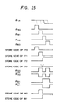
- Fig. 34 shows a circuit configuration of the column register of another embodiment of the present invention.
- Fig. 19 and Fig. 20 show the operation time charts thereof.
- the second group of storage cells 280, 281 is composed of 4-MOST type memory cells.
- the 4-MOST type memory cell is provided with two data lines in order to execute the differential type reading and writing operations. Accordingly, as shown in Fig. 35, the control signals ⁇ D 0 , ⁇ D 1 must be used as the complementary signals of ⁇ D0 and ⁇ D1 on the occasion of writing the data corresponding to timing of voltage change of the input signal ⁇ in into the cells 280 and 281.
- the switch 287 in Fig. 27 is unnecessary and the switch 293 is required.
- the switch 293 is OFF for writing the data corresponding to the timing of voltage change of the input signal ⁇ in or ON in other cases.
- This embodiment is superior in the operation speed and noise margin because reading from the second group of storage cells is carried out in the differential mode.
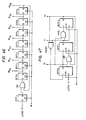
- Fig. 37 is a circuit diagram of column register indicating further embodiment of the present invention.
- the second group of storage cells 28O, 281 is formed by the 1-MOST type memory cell.
- This embodiment has an advantage that the second group of storage cells occupies only a small area.
- the 1-MOST type memory cell is not provided with the amplification function in itself and therefore it requiries the amplifiers 37O and 371 for amplifying the signal read from the cells 28O,281.
- the column register of the MLS memory of the present invention is capable of externally reading the data stored in the group of storage cells of the one column and simultaneously writing external data into the group of storage cells of the one column and also storing the multiple level signals in a small number of cells, thus realizing high speed data transfer and parallel writing and reading.
- the present invention also provides a fault tolerate circuit which is just suited to the memory which serially executes data reading and writing.
- Fault tolerate can be done as explained below in the memory which serially reads and writes the data.
- the "location" of defective memory cell among the regular memory cells, namely in which number the defective memory cell is selected during the serial reading and writing is previously written into the ROM (Read Only Memory).
- ROM Read Only Memory
- content of data written in the ROM is compared with a number of times of data reading (writing). In case these are matched, the regular memory cell is not selected and the spare memory cell is selected.
- Fig. 38 shows an embodiment of the present invention.
- a counter 387, ROM's 388 and 389, comparators 390 and 391, and a switching circuit 392 are provided as explained previously. Since two spare data lines are prepared, ROM and comparator are also provided in two each for respective spare. This embodiment is explained in detail hereunder.
- the address signals a0 ⁇ a m-1 are decoded by the decoder 382 and only one word line among the lines W0 ⁇ W M-1 is selected by the word line drive circuit 383. For example, when W i is selected, data is read on the data lines D0 ⁇ D N-1 from all memory cells MC i0 ⁇ MC iN-1 on the W i . This signal is amplified and output by the read lines SA0 SA N-1 .
- this memory array 381 and read circuits SA0 ⁇ SA N-1 there are the circuits, for example, shown in Fig. 1, Fig. 11 and Fig. 26.
- the static memory can also use the fault tolerate system described below.
- the data lines D0, D1 ??, D N-1 are selected in this sequence in sychronization with the clock pulse ⁇ .
- the data line select circuit 384 must provide one output of logic "1" and logic "0" among the N outputs ⁇ YA0 ⁇ YA N-1 .
- This can be realized, for example, by forming a shift register through connection of (N + 1) D flip-flops DFF ⁇ 1 DFF N-1 as shown in Fig. 39. Namely, only DFF ⁇ 1 is set to logic "1", other DFF0 DFF N-1 are set to logic "0” and the clock pulse ⁇ is applied N times. After the pulse ⁇ is applied (j + 1) times, only the ⁇ YAj becomes logic "1" and the data line D j is selected.
- an n-bit binary counter utilizing the JK flip-flop (JKFF) as shown in Fig. 40 can be used.
- JKFF JK flip-flop
- the memory For data reading or data writing to/from the memory, the memory is set so that when outputs X0 ⁇ X n-1 become "-1" when it is considered as the binary numbers, namely all bits become logic "1" and the pulse ⁇ which is the same as the signal to be applied to the data line select circuit 384 is applied.
- the pulse ⁇ When the pulse ⁇ is applied first, the outputs X0 ⁇ X n-1 are "0", namely all bits becomes logic "0".
- the bits change to "1", “2", ... for each application of the pulse ⁇ . Accordingly, after the pulse ⁇ is applied for (j+1) times, and-output of counter becomes "j" (as explained above, the data line D j is selected at this time) and it can be used as the index of indicating the currently selected data line.
- Fig. 41 shows the structure of a pair of ROM and comparator.
- ROM ROM
- EPROM EPROM
- E2PROM or a fuse to blow by laser can be used but the fuses F0 ⁇ F n which blows electrically are used here.
- the fuse F k blows by means of a MOS transistor Q k0 .
- a latch circuit LT k is formed using two enhancement type MOS transistors Q k1 , Q k2 and depletion type MOS transistor Q k3 .
- An output y k of the latch circuit LT k is set to the high level (logic 1) when the fuse F k has blown or is set to the low level (logic 0) when the fuse F k is normal.
- the outputs y0 ⁇ y n-1 of latch circuit are compared with the outputs X0 ⁇ X n-1 of said counter by the exclusive OR gate (EOR k ) and NOR gate (NOR).
- a number of fuses is set to (n+1) in place of n because one fuse (F n in Fig. 7) is required for identifying whether fault toleration should be conducted or not.
- the fuse F n In case fault toleration is not conducted, the fuse F n is kept normal. Thereby, an output ⁇ c is always logic 0.
- a fuse F n In case fault toleration is conducted, a fuse F n is blown, and the fuses F0 ⁇ F n-1 are determined whether they should be cut or not in accordance with the location of data line to be tolerated as explained above.
- Fig. 42 shows an example of circuit structure. This circuit switches between the regular data line and spare data line in accordance with the outputs of said comparators ⁇ c0 , ⁇ c1 .
- the MOS transistors Q1, Q2 are ON and Q3 Q5 become OFF. Therefore, data transfer is carried out between the data line selected bh the data line select circuit 4 and the input buffer 385 or output buffer 386 through the regular input-output line I/O', I/O' .
- fault toleration is not carried out for the word lines.
- one word line can be selected arbitrarily by the decoder 2 and therefore fault tolerate of word lines can also be done in the same way as the existing method.
- Fig. 43 shows this example where the reading or writing is carried out to N/4 memory cells among N memory cells on the single word line in the embodiment of Fig. 38. This embodiment is described in detail below.
- the memory array 381, decoder 382, word line drive circuit 383 and read circuits SSA0, SSA1, SA0 ⁇ SA N-1 are provided as in the case of embodiment of Fig. 38.
- the data line D4+1 is selected.
- the data line D4 +2 is selected.
- the fault tolerate circuit of the present embodiment is now explained.
- the (n-2)-bit binary counter is used.
- the outputs X2 ⁇ X n-1 of counter can be used as the index which indicates which data line group is now selected as in the case of Fig. 38.
- ROM's 388 and 389 are the same as those shown in Fig. 41.
- each fuse should be blown so that the outputs y2 ⁇ y n-1 among the outputs y O ⁇ y n-1 of ROM indicate the location of data line group including the data line to be fault-tolerated and y O , y1 indicate the location of such data lines in the data line group (namely, the line is selected in which combination of a m and a m+1 ).
- Fig. 44 shows the structure of comparator.
- the circuit structure itself is the same as that shown in Fig. 41 but there is such a difference that the address signals a m , a m+1 are input in addition to the outputs x2 ⁇ x n-1 of counter.
- the switching circuit 392 is the same as that shown in Fig. 42 and therefore explanation thereof is omitted here.
- Fig. 45 shows another embodiment of the present invention.
- This embodiment is characterized by providing redundant bits by the error correcting code (hereinafter referred to as ECC).
- ECC error correcting code
- the ECC uses 4 information bits, 3 check bits and cyclic Hamming code and other codes can of course be used for the present invention.
- D0 to D3 are used as the inforamtion storing and D4 ⁇ D6, for storing redundant bits of ECC.
- the redundant bits for ECC are added in the encoding circuit 450 and error correction is carried out in the decoding circuit. This embodiment is explained in detail.
- the memory array 381, decoder 382, word line drive circuit 383 and sense amplifiers SSA0, SSA1, SA0 ⁇ SA N-1 are provided as in the case of embodiment shown in Fig. 38.
- the data-line select circuit 384 must be capable of selecting not only the data line for storing information but also the data line for storing redundant bit of ECC. Moreover, as described later, in the case of data reading operation, the data line must be selected twice in each operation in the sequence of D1, ...., D6, D0, D1, ..., D6.
- Fig. 46 shows an examle of circuit which satisfies such requirement.
- the encoding circuit 450 his explained hereunder. This circuit executes encoding serially in synchronization with the clock pulse ⁇ using the nature of cyclic code.
- the clock pulse ⁇ is first applied four times, the data entering from external input terminal D in through the input buffer 385 is directly issued to the input-output line I/O (at this time, redundant bit is also generated simultaneously).
- the clock pulse ⁇ is applied three times in succession (in this case, data is not input from D in ), the generated redundant bits are sequentially issued to the I/O.
- the data line select circuit 4 selects the data lines in the sequence of D0, D1, ..., D6, the information bits(data entering from D in ) is written into the memory cells on the data line D0 ⁇ D3, while the redundant bits to the memory cells on the data lines D4 ⁇ D6.
- the decoding circuit 460 is described. This circuit executes the decoding serially in synchronization with the clock pulse ⁇ , using the nature of cyclic code.
- the clock pulse ⁇ is first applied seven times, the data lines are selected in the sequence of D0, D1, ...., D6 by the data line select circuit 388 and the data read from each memory cell is sequentially applied to the decoding circuit through the input-output line I/O.
- 460 executes the calculation of syndrome.
- the clock plulse ⁇ is applied seven times, the error corrected data are sequentially issued to the input-output line I/O.
- the data lines D0 , D1 ...., D6 are selected again in this sequence by the data line select circuit 384 and therefore the corrected data is sequentially written into the original memory cell.
- the first four bits (information bits) among the corrected data are sequentially issued to the external output terminal D out through the output buffer.
- the fault-tolerate circuit of this embodiment is explained.
- the counter 387 is described below.
- the data lines are selected in the sequence of D0, D1, ...., D6, and thereby output of counter 387 must be changed in the sequence of "0", “1",....,”6", "0", "1",....,”6".
- the ROM's 388 and 389, comparators 390, 391 and switching circuit 392 are the same as those shown in Fig. 42.
- the ROM since total of seven data lines are prepared including the redundant data lines for ECC, the ROM requires 4 bits (one bit of them is used for identifying whether fault tolerate must be conducted or not) and the exclusive OR gate of comparator requires three bits.
- the present invention can introde the fault toleration for the memory which serially carries out data reading and writing and thereby a chip containing a small number of defects can be converted to a good chip,thus improving the yield.
Description
- The present invention relates to a semiconductor memory and particularly to a semiconductor multilevel memory having multiple storage levels of information per memory unit even under a low power supply voltage and cnsumes less electrical power.
- A semiconductor memory having a higher integration density, represented by a dynamic random access memory (hereinafter abbreviated as DRAM), has been developed year after year and a memory unit of semiconductor memory (hereinafter referred to as memory cell) and peripheral circuits are more and more superminiaturized. However, improvement in integration density by such superminiaturization must usually be accompanied by a large stride of advancement of element process technology such as photorithogrphy and etching, etc. and therefore a certain period is usually requried for devlopment of element process technology.
- Meanwhile, demands for very high density semiconductor memory are increasing continuously and for example, a semiconductor memory having a large capacity and less power consumption is craved for newly developed field such as a small size office computer and the terminals thereof which have recently showed fantastic growth. Namely, an existing semiconductor memory is said not only as it is insufficient from the point of view of integration density but also in sufficient from the point of view of power consumption and other performances.
- In order to meet such requirements, a memory having multiple level storage structure (MLS memory) is considered as an effective means for realizing a semiconductor memory having a higher integration density by the current process technology. This memory is intended to substantially increase integration density by causing a single memory cell to store the data of more than two (2) levels.
- As an MLS memory, a charge transfer device (hereinafter referred to as CTD) is well known. These are explained in detail, for example, in L. Terman tal. IEEE Journal of Solid-State Circuits. Vol. sc-16, No. 5, pp.472-478, October 1981. and M. Yamada et. al. Proceedings of the 9th Conference on Solid-State Devices, Tokyo 1977, pp. 263-268, issued on January 1978.
- However, the MLS memory using CTD is not yet often put into practical use, because a number of levels cannot be increased so much in order to prevent that a multilevel data of analog signal is substantially attenuated due to finite transfer efficiency peculiar to the CTD. Or, such multilevel memory is inferior in such a point that it is necessary to raise a driving pulse voltage in order to increase the transfer efficiency and such element intrinsically has a high capacitance load and consumes a very high electrical power. Moreover, it is also inferior in such a point that a memory cell can be formed small because high precision A/D, D/A converters are required for loops of each CTD but integration density cannot be raised due to the restriction on the peripheral circuits.
- A MLS memory is also disclosed in FR-A-2 246 022. The read circuit described in this document, however, is only reliable if the storage capacitor is considerably larger than the capacity of the data lines and the input capacity of the read circuit.
- In EP-
A-0 139 196 a charge transfer amplifier is described which amplifies the signal voltages on the data line with high accuracy. - Further, EP-A-0 130 614 discloses a MLS memory in which a multi-level step voltage is applied to the plate electrode of the storage capacitor or to the gate electrode of the associated MOS-FET of the memory matrix for reading and writing data of more than two voltage levels from or into the capacitor.
- The latter two prior art documents are not prepublished and fall under Article 54(3) EPC.
- The inventors of the present invention have thought that a dynamic memory (DRAM) for addressing by both rows and columns is caused to store the multiple level data as an MLS memory for eliminating various disadvantages of an MLS memory using CTD described above and the A/D, D/A converters are also provided in the sensing and writing sytems. In the case of the memory for addressing by both rows and columns, it is no longer necessary to consider the transfer efficiency, a number of gates to be driven can be decreased and thereby power consumption can also be saved. However, a very difficult problem explained below must be solved in order to use such DRAM as an MLS memory. Namely, even if multilevel data(analog signal) of the maximum dynamic range (multilevel data can be obtained by dividing it) of 5 Vpp is stored in the memory cell, a parastic data line capacitance is often larger than the capacitance of memory cell in the order of one digit and therefore if it is read on the data line, the maximum dynamic range becomes as low as 500mVpp or less. It is very difficult, however, to mount many A/D converters which amplifiy small analog signal with high accuracy and convert it into digital value, except the case where a number of levels of multilevel signal is low. Particularly when it is very difficult to provide the A/D converter for each data line if the data line pitch is not rough.
- Here, it should be noted that a MLS memory can be used as an excellent large capacity memory when a number of memory cells which is equal to or larger than that of an ordinary 2-level memory are mounted on a chip in such a size as is equal to or smaller than that of said 2-level memory. Namely, when current signal charge of one memory cell of DRAM is Qs', if the manufacturing process technique is equivalent, a signal charge allowed for one level of multilevel memory becomes about Qs'/N when a number of level is N. It is a very severe condition. Accordingly, an amplifier which can amplify a minute signal with high accuracy and a small size A/D converter with high accuracy are simultaneously required for an MLS memory for addressing both rows and columns. But such amplifier and converter cannot be realized and accordingly an MLS memory of this type cannot be developed.
- It is an object of the present invention to realize a new memory having multiple level storage structure (MLS memory) for addressing by both rows and columns and thereby provide a large capacity semiconductor memory with less power consumption.
- In order to attain the above object, the present invention provides an MLS memory comprising a newly developed minute voltage amplifier which is just suited to a large capacity memory, a highly accurate A/D, D/A converting structure even with simplified configuration and low power consumption and peripheral circuit with less power consumption. Thereby, it is now possible to replace a magnetic disk unit which requires large physical occupation and electrical power with a semiconductor memory, for example, in a small size computer system.
- Fig. 1 is a block diagram of an embodiment of the present invention. Fig. 2 is a schematic diagram for explaining the A/D conversion during the read operation by an MLS memory as the embodiment of the present invention. Fig. 3 is a schematic diagram for explaining the D/A conversion during the read operation by an MLS memory as the embodiment of the present invention. Fig. 4 is a circuit diagram of an embodiment of colum register of the present invention. Fig. 5 shows pulse timing of the embodiment shown in Fig. 4 of the present invention. Fig. 6 is a sectional view of an embodiment of the BCT amplifier. Fig. 7 shows the timings (A) and potentials (B-1 5) of pulses for driving the amplifier of Fig.6. Fig. 8 shows the timings (A) and potentials (B-1 to B-6) of the same pulses. Fig. 9, Fig. 10, Fig. 25 show sectional views of other embodiments of BCT amplifier. Fig. 11 shows an embodiment of the signal sense circuit of the present invention. Fig. 12 shows drive pulses and internal waveforms used in Fig. 11. Fig. 13 shows a circuit diagram of sense amplifier by another embodiment of the present invention. Fig. 14 shows drive pulses and internal waveforms used in Fig. 13. Fig. 15 shows a circuit diagram of sense amplifier by the other embodiment of the present invention. Fig. 16 shows drive pulses and internal waveforms used in Fig. 15. Fig. 17 shows operation waveforms of the present invention. Fig. 18 and Fig. 19 show circuit diagrams of decoder and encoder by the embodiment of the present invention. Fig. 20 shows timings of drive pulses used for the encoder shown in Fig. 19. Fig. 21 shows a circuit diagram of triggering pulse generator by an embodiment of the present invention. Fig. 22 shows internal waveforms in Fig. 21. Fig. 23 shows another embodiment of the present invention. Fig. 24 shows drive pulses used in Fig. 23. Fig. 26 shows a circuit diagram of another embodiment of the present invention. Fig. 27 shows a structure of column register indicating an embodiment of the present invention. Fig. 28, Fig. 29 and Fig. 30 respectively show operation time charts in Fig. 27. Fig. 31 shows a structure of column register indicating another embodiment of the present invention. Fig. 32 shows time charts of the circuit shown in Fig. 31. Fig. 34, Fig. 37 respectively show structures of colulmn registers indicating other embodiments of the present invention. Fig. 33, Fig. 35 and Fig. 36 show operation time charts. Fig. 38, Fig. 43, Fig. 45 show structures indicating embodiments of semiconductor memories comprising a fault tolerate circuit by the present invention. Fig. 39 and Fig. 46 show circuit diagrams of data line addressing circuit used in said memory. Fig. 40, Fig. 47 show a counter circuit used in said memory. Fig. 41 shows a circuit diagram of ROM and comparator used in said memory. Fig. 42 shows a circuit diagram of switch circuit used in said memory. Fig. 44 shows a circuit diagram of comparator used in said memory.
- The present invention is explained by referring to the preferred embodiment thereof. In the following embodiment, data is carried and stored by the operations of electrons used as signal charge carriers but the holes can also be used in the same way by changing the polarity of power supply and pulses and the conductivity type of semiconductors.
- Fig. 1 shows a block diagram of an embodiment of an MLS memory by the present invention. In this figure, numeral 1 is unit cell (hereinafter referred to as memory cell) of memory. 2 is storage capacitor. 3 is switching transistor (switching MOS transistor) which operates as word gate. 4 is electrode of
storage capacitor 2 which is usually connected to a DC power supply (Vcc) and earth (Vso). 5 is word line. 6 is data line. 7 is block of memory cell array. 11 is unit of dummy cell. 12 is dummy storage capacitor which is selected to 1/2 of information storage capacitor Cs. 13 is switching MOS transistor which operates as dummy cell selection gate. 14 is electrode of dummy storage capacitor which is used in common as the electrode of storage capacitor of memory cell. 15 is word line of dummy cell. 17 is block of dummy cell array. 18 and 19 are reset gate and reset gate line of dummy cell. 30 is reset gate of data line. 31 is write gate. 21 is array block of 30 and 31. The write gate among various gates is composed of a p-channel MOS transistor, while the others are composed of an n-channel MOS transistor. In the following figures, the p-channel MOS transistor is indicated by giving an arrow mark to the source thereof
and the n-channel MOS transistor is indicated only by
32 is bias charge transfer amplifier (hereinafter referred to as BCT amplifier) which amplifies with high accuracy the signal voltages on the data line which has been divided into multilevel low voltages up to large voltages. 22 is block of array. 33 is sense amplifier. 23 is array block thereof. 34 is column register (temporary storage cell). 24 is array block thereof. 35 is a triggering pulse generator. 36 is multiple-level step voltage generator. 37 is control circuit which controls thesense systems - In an embodiment of an MLS memory shown in Fig. 1, A/D, D/A conversion means is realized a multiple-level
step voltage generator 36 and ashift register 38 which are controlled by a triggeringpulse generator 35, arow address buffer 25 which transfers multiple-level step voltage to theword line 5, amemory cell 1, areset gate 30, writinggate 31, acolumn register 34, an input-output circuit 27 and a decoder/encoder 28. - Said A/D, D/A conversion means is explained first hereunder.
- In the following explanation, a number of multiple levels is set to four levels (2 bits) but in actual it is possible to select more large number of levels.
- Fig. 2 shows a schematic diagram for explaining the A/D conversion means of multiple level memory of the present invention under the data reading operation. In the same figure, 41 is a stepping voltage pulse (φw) to be applied to the
word line 5. V is the positive direction of voltage. 42 is electron potentiala EP ofmemory cell 1. 44 corresponds to a potential ofstorage capacitor 2, while 45 to that ofword gate data line 5, respectively. The lower side indicates the positive direction. 47 is an electrode ofstorage capacitor word gate 3. 43 is a column register of multiple level data and there are four cells corresponding to multiple levels. Here, it is supposed that the second level "2" of charge storage states ("10" in the binary data) is stored in the storage capacitor. When the stepping pulse φw to be applied to theword line 5 is sequentially raised corresponding to the times t₁, t₂, t₃.... no signal charge is generated up to the time t₁∼t₃ but the signal charges are read on thedata line 6 at the timings t₃∼t₄ and t₄∼t₅. The signal read out is amplified and then sent to the column register. At the timing t₁∼t₃, no charge is generated and therefore the "vacant" data OFF is sent the thecolumn register 43. Since charges are output at the timings t₃∼t₅, the "existing" data ON is sent to thecolumn register 43 and is then stored in the corresponding cell. As will be described later, when once data is stored in a cell of column register in this example, writing is not executed to the successive cells. Therefore, as shown in the figure, multiple level data stored in the memory cell is stored only to the cell at the position "2" among the cells of column register. - The multiple level data readout above is no longer analog data but the digital data. This digital data is sent to the encoder through the output lines (in this example, used as the input-output common line (I/O line); refer to Fig. 4, Fig. 11, Fig. 18, Fig. 19) and is then read as the usually employed digital data such as binary code.
- Above A/D conversion system is characterized in that after signal charge is output from memory cell, a charge packet only carries a binary digital data of ON and OFF, and multiple level data is effectively carried at the timings t₁∼t₅ which are given by the pulses sent from the triggering pulse generator which control the column register and the pulse φw applied to the word line. Thereby, signal voltages on the data line does not require amplification of high precision analog value which is required for ordinary A/D conversion and can be processed as 2-level data for ordinary memory.
- Accordingly, the A/D conversion system of the present invention does not become a large scale and high power circuit which interferes realization of high integration density memory like the existing A/D conversion circuit and a memory with super-high integration density can be realized with less power consumption.
- Fig. 3 shows a schematic diagram indicating the D/A conversion means of MLS memory of the present invention under the writing operation. In this figure, 51 is the stepping pulse (φw) to be applied to the
word line 5. 52 is electron potential ofmemory cell 1, corresponding to thepositions 44∼46 andelectrodes - In the writing operation; a data line is set to a low level (0V in this case) by the reset gate 30 (t₆∼t₇). When it is required to write the second level "2" of charge storage states, the data line is raised to a high level through the
write gate 31 when the pulse /w reaches the corresponding level (t₈∼t₉). Thereby, the second level "2" is remained as indicated by 53 in the memory cell. The write pulse decodes the write data and is given to thewrite gate 31 through thewrite lead 39 at the dependent timing. Since the D/A conversion for writing is carried out also in this case at the timing (t₇∼t₁₁), the circuit structure is very simple, high integration density can be realized and power consumption is very low. - The write-read means shown in Fig. 3 and Fig. 2 have such a large characteristic that the signal charges corresponding to a level does not almost change depending on the location when the level of pulse φw does not change in accordance with the position because the write and read operation to/from the data storage capacitor is carried through the
same gate 3. Namely, a storage capacitor is Cs, a threshold voltage ofgate 3 is VThs, a voltage of pulse φw in the writing operation is VW, a voltage of pulse φw in the reading operation is VR, a voltage Vs of storage capacitor when data is written becomes


- When substrate voltage effect is low, Qs becomes constant, irrespective of VThs. Therefore, if a threshold voltage VThs of memory cell disperses in places, the signal charge Qs is almost constant and data can be judged accurately. It is very important for an MLS memory having a large number of levels because a level is selected in such order near the dispersion of threshold voltage of MOSLSI chip in such a case that a stepping voltage φw (Δφw) is set, for example, to 200 mV or less.
- Fig. 4 and Fig. 5 show respectively the practical example of circuit diagram of the column register, column address select gate (Y gate) and input-output circuit block 27 (herein after explained as a part of column register) in the embodiment shown in Fig. 1 and the pulse timing chart.
- In Fig. 4, 61 is a shift register corresponding to a control circuit which controls a
storage 38 shown in Fig. 1. This register sends the pulse φSR shown in Fig. 5 to the column register. - Fig. 5 shows the drive pules and internal waveforms in the READ/REFRESH mode of the MLS memory of the present invention. In this example, the data "2" is read and the same data is written again. First, the read
gates 620 623 are precharged to a high level through theprecharge gate 63 at the timing t₀. At the timing t₁∼t₅, the ascending stepping pulse is applied to the word line 5 (Fig. 1), signal charge is read to thedata line 6 when the level is R₂ (t₃∼t₄) and a voltage V₀ drops (71). This signal is amplified by thevoltage amplifier 32, judged by thesense amplifier 33 and appears on theoutput terminal 64 as an output voltage Vso (72). This process is explained in detail later by referring to Fig. 11 and Fig. 12. Therefore, a voltage ofcommon electrode line 62 is lowered through the gate 60 (73), and a high level being given as φR2 is is stored in the temporary storage node 65 (tR2). When the level is R₃ (t₄∼t₅), charges appear on the data line (74) and an output appears at Vso in the process similar to that mentioned above. But, since VLG is already lowered to a low level, a high level voltage does not enter thenode 66. - Next, a voltage VD of
data line 6 is reset to a low level (76) by thereset gate 30 at the timing t₅. The descending stepping pulse is aplied to theword line 5 and the pulse φSR is sequentially applied as φW0 φW3 from the shift register 61 (t₇∼t₁₁). At the timing t₈∼t₉, when the pulse φW2 becomes high level, aMOS transistor 67 becomes conductive since a high level has been stored in thenode 65 ofgate 67 during the READ cycle anda voltage VRF ofrefresh line 68 becomes high level (77). At this time, since thenode 65 is in the high impedance, VRF can be boosted up to a high level as in the case of φW2 without any influence of the threshold voltage, owing to the bootstrap effect by the capacitance 69 (including gate channel capacitance) between the gate and source. - The timing of level "2" output to VRF as indicated as 77 also appears on the I/O line through the
Y gate 70 if this column is selected by φYA. In this case, it is read as the 2-bit binary signal by sending it to the encoder to which the pulse being synchronized with φW3 φW0 is supplied. - On the other hand, an
output V RF 77 gives an inverted output (low level) to the writing gate 31 (Fig. 1) consisting of the p-channel MOS transistor by means of aninverter 59. Thereby, a voltage V₀ of data line is raised up to high level (78) and the level W₂ is stored in the memory cell as shown in Fig. 3 (53). Namely, this operation is called REFRESH operation. - During the REFRESH operation, the write enable signal φWE (Fig. 4) is set to low level and writing is not carried out externally. If it is required to write data externally, the signal φWE is set to high level and the signal VLG is set to low level, thereby the function of column register is disabled, the multiple level input signals obtaned by the decoder in the I/O line side are input in the timings φW3 φW0 and thereby the data can be written externally into the memory cell through the
REFRESH line 68. - A temporary storage (column register) providing N (or N-1) storage cells corresponding to a number of levels N has eliminated, when it is installed, a large scale circuit such as encoder, decoder and logic gate (exclusive OR gate and AND gate) required for refresh operation from each data line and is very important component which realizes the sense system of MLS memory with such an integration density as the DRAM in the maximum integration level. This storage has attained practically the high integration density MLS memory of the present invention for the first time. In Fig. 4, the
precharge gate 63 among various gates uses the p-channel MOS transistor, while the other gates use the n-channel MOS transistors. - As is already described, it is substantially important for the MLS memory for addressing by both rows and columns to amplify with high accuracy the signal per level which has been divided into minute signals of multiple levels. In the present invention, such requirement has been attained by providing a high performance bias charge transfer amplifier shown as 32 in Fig. 1 and an MLS memory which realizes a large number of multiple levels even at a low voltage has been embodied for the first time.
- Fig. 6 is a sectional view of BCT amplifier (bias charge transfer amplifier) which amplifies a minute signal of one level appearing on the data line up to such a voltage as can be sensed by the
sense amplifier 33 consisting of the MOS transistor circuits. Fig. 7 shows drive pulse timings and potentials. Fig. 8 shows pulse timings and potentials indicating other driving method. Fig. 9 and Fig. 10 show the embodiments of BCT amplifier. - In Fig. 6, 80 is an insulating film; 81 is an N type semiconductor substrate; 82 is a P-type well region; 83 86 are n⁺ layers; 87, 89 are charge transfer gates; 88 is a charge driving gate; 90 is a precharge gate; 92 is a sense amplifier input terminal.
- Operations of BCT amplifier are explained by referring to Fig. 6 and Fig. 7.
- First, the
reset gate 30 is set to the conductive state (ON state) by the reset pulse φR, resetting thedata line 60 to 0V or a sufficiently low voltage. Next, after thegate 30 is set to non-conductive state (OFF state), thegates 87∼89 and 90 are set to the ON state and the potential ofdata line 6 is set to
gate 87, VThT3 is a threshold voltage (including substrate effect) of thegate 87. Thegates 87 89 are then set to the OFF state and a bias charge stored under thedrive gate 88 is also set (Fig. 7(B-2)). At this time, the signal charge carrier ofstorage capacitor 2 is read on the data line through the word gate 3 (93 of Fig. 7(B-2)). Then thegate 87 is set to ON state and the bias charge at the lower part ofdrive gate 88 is moved to the side of data line 6 (Fig. 7(B-3)). A capacitance (CD) ofdata line 6 is considerably large among the node capacitances within the apparatus and often takes an order of PF. But, a capacitance ofdrive gate 88 is very small as compared with it. Therefore, the drive charge is mostly moved to the side of data line. At this time, a bias charge mixes with signal charges. Next, thedrive gate 88 is set to ON state and such mixed charges are fetched to the lower part of drive gate 88 (Fig. 7(B-4)). Moreover, thetransfer gate 87 and drivegate 88 are set to OFF and charges are transferred to theinput end side 92 of sense amplifier 92 (Fig. 7(B-5)). At this time, a voltage is is applied to thegates 87∼89 in the same condition as (B-2) and the bias charge is not transferred and only the signal charge is transferred as 94∼95. - The drive pulse timing is shown in Fig. 7(A). Said bias charge transfer process is repeated for a number of times corresponding to a number of levels 9 (for example, 4 times in the case of four levels) for reading multiple level data reading. Namely, in the example of Fig. 2, the bias charge transferf is carried out once during the timing t₁∼t₂ and the timing t₂∼t₃ respectively. Such repetition may be allowed during the timing t₂₃∼t₂₈ as shown in Fig. 7(A) or may be allowed during the timing t₂₁∼t₂₈, except for the reset time of data line. Durting the latter timing, the bias charge under the
drive gate 88 is reset in each timing and therefore when reading is conducted many times, the bias charge transfer can always be done with high accuracy by preventing that the charges are reduced by a tailing current of the gate T1 (89). - Here, a minute charge Qs on a large capacitor CD can be efficiently moved to a small capacitor C₁ by the following reason.
- Namely, the gate T3 (83) becomes cut-off state, a current usually does not almost flow under the gate T3 because a voltage amplitude is very small even when a minute signal appears on the data line as indicated by 93. It is because the gate T3 is in the tailing region at a very low level. However, when a bias charge is sent onto the data line, the operating point of tailing rises and a current which is as large as different order flows and for example, charges of about 99% move to the lower side of gate T2. In this charge, the signal charges of 99% are also included and when the bais charges are subtracted through the gate T1 (89), the signal charges can be moved to the sense
amplifier input terminal 92 with a very good transfer efficiency. - In above charge transfer; transfer of signal charges can be done for each gate under the saturated mode as indicated by (B-4), (B-5). If such transfer is carried out under non-saturated mode, transfer of signal charges is not conducted sufficiently due to the division of capacitance.
- Fig. 8 shows another driving method. This method is different from Fig. 7 in such a point that setting (B-3) of bias charge and transfer of such bias charge to the sense amplifier input terminal through the gate T1 (89) from the gate T2(88) are conducted under the condition that both T1 and T2 are ON. Thereby, the OFF level of each gate T1, T3 is simple cut-off state and it is not required to think of the conductive state of current. Thus, low level setting of pulse can be done easily (in many case, it can be set to 0V). Each reset of bias charge under the gate T2 described in Fig. 7 is carried out by setting the terminal 91 to low level in (B-2). In case charges are transerred many times, operations are more stabilized by repeating the steps (B-2) - (B-6) (t₃₂∼t₄₁). Here, the timing (t₄₀) for making high level the pulse φT1 may be set to the timing t₃₈∼t₃₉ (B-5) where the pulses φT2 and φT3 are high level as shown by 96. Thereby, even when the capacitance of gate T2 for tee signal charges is small, the signal charges do not appear under the gate T2 and charges are sent to the sense amplifier input terminal through the gate T1.
- Fig. 9 shows another embodiment of structure of BCT amplifier which is different from that of Fig. 6 in such a point that n⁻ or n⁺
layer 101 is provided under the gate T2 (88). As is apparent from the potential diagrams of Fig. 7, Fig. 8, it is better that the gate T2 (88) as the lowest threshold voltage VThT2 among those of the gates T1(89) and T3(87) and it is the depletion type. If it is the depletion type, the drive pulse φT2 can be simplified as the maximum voltage (Vcc) of the 0V system. When the threshold voltages of gates T1 T3 are considered as VThT1∼VThT3, the gates T1∼T3 can be driven with the drive pulse of high level, low level and equal amplitude as is obvious from Fig. 7(B-1), Fig. 8(B-1) when there are relations, VThT3 > VThT1 > VThT2, VThT2 < 0V, (VThT1 < 0V). Incase 101 is the n⁺ type, the gate T2 becomes only a simple capacitor, but as is apparent from operation principle of Fig. 7 and Fig. 8, the same effect as that obtained when the gate T2 is a MOS transistor can also be obtained. - Fig. 10 is an embodiment where the tate T2 is considered as a capacitance (formed by the
electrodes 102 and 103) on the field by considering it as only a simple capacitance. Thereby, the processing for providing the n⁻ or n⁺ layer under the gate T2 is no longer necessary and the manufacturing process can be matched with that for ordinary memory LSI. - If the gate T2 is formed as the enhancement type, when the low level of drive pulse φT2 is set to 0V, recoupling of electron and hole pair occurs through the surface level at the semiconductor surface under the gate and charge transfer efficiency is deteriorated. But it can be prevented by setting low level of φT2 to a value higher than VTht2 or by applying a negative bias to the
well 82. - In the embodiments of Fig. 9 and Fig. 10, such phenomenon does not occur and low level of φT2 can be set to 0V.
- Fig. 25 shows an embodiment indicating another structureof BCT amplifier which is different from the preceding embodiment in such a point that the gate T1 is eliminated. In this case, the bias charge under the gate T2 (88) is given by a voltage to be applied to the terminal 91 through the precharge gate. When the pulse φT2 is set to low level, the bias charge is sent and it is set to high level again. Thereby, it is obtained together with the signal charage, as in the case of the preceding embodiment. At this time, the bias charge and signal charge are sent to the sense amplifier while these are mixed and these are judged. Since the input capacitance of sense amplifier becomes large, the amplification coefficient is not so large but structure can be simplified.
- Fig. 11 shows practical example of circuit structure of the signal sense system as a whole of the MLS memory of the present invention. Fig. 12 shows the drive pulse waveforms and internal waveforms. In these figures, the elements given the same symbols such as 32, 33, 34, 27, 61, t₃, t₄, t₃₁∼t₄₁, etc. indicate the same elements and timings, etc.
- The timing waveforms shown in Fig. 12 indicate the condition that the data "2" is just stored in the memory cell and it is then extracted, considering the case where the cell connected to the
data line 6 is selected ata the memory cell and a dummy data (in such an amount equal to 1/2 of signal charge) appears from the side ofdata line 6D. In such figure, DP is a drive pulse and IW is internal waveform. - When a voltage (φw) of word line rises to the level "2" (t₃) from the level "1" (R1), charges are read on the
data lines dummy word line 15, charges equal to Qs/2 is sent each time to thedata line 6D for each rise of one step of word line voltage from the dummy cell. Meanwhile, since the signal charge Qs appears on thedata line 6, a voltage ofdata lines

- During the timing t₃₇∼t₃₉, the data line voltage VD and data line voltage of dummy data VDD return to the original volates respectivelyu due to the bias charge transfer and the signal charge and dummy charge are respectively sent to the sense
amplifier input terminals - Prior to this operation, the voltages VSA, VSAD of sense
amplifier input terminals - When the pulse φFA1 turns ON at the timing t₄₂, the flip-flop type (hereinafter referred to as FF type) sense amplifier starts, a voltage VSA is dropped to low level (0V) and VSAD is also dropped (t₄₂∼t₄₃). Next, when the pulse φFA2 becomes low level, the P-channel MOS transistor QFA2 becomes conductive, raising VSAD to Vcc and the judging operation of sense amplifier is defined (t₄₃∼t₄₄). Since the pulse φFA2 makes conductive Q₉₂, Q92A, an output of the sense amplifier is sent to the column register. The pulses a₁,
a₁ determine to which line of a pair ofdata lines 6 6D the signal charge and dummy charge are output. In this example, the pulse a₁ is high level, while the pulsea₁ is low level. Accordingly, VSAD defined to be high level raises a voltage Vso ofnode 64 through the transistor Q64D and thereby a voltage VLG of readgate 62 is also raised (t₄₃∼t₄₄). At this time, since the output φR2 of shift register is in the high level, a high level voltage is stored at the source end (65 of Fig. 4) of read gate as in the case of Fig. 4 and the multiple level data can be read. This data can be read to the external circuit, refreshed and written externally as explained with reference to Fig. 4 and Fig. 5. - The FF type sense amplifier shown as 33 in Fig. 11 has the input dynamic range as wide as Vcc to 0V and quickly amplifies the signal, owing to the positive feedback. As described later (Fig. 17), the signal appearing on 92, 92D easily has the offset due to the characteristic of BCT amplifier. Therefore, wide input dynamic range is just suited for the MLS memory of the present invention and accordingly more reliable operation of the sense system of MLS memory can be obtained.
- Fig. 13 shows a differential type high sensitivity amplifier as another embodiment of sense amplifier of the present invention. Fig. 14 shows drive pulse timings and internal waveforms.
- After the voltages VSA and VSAD of 92, 92D are lowered to 0V by the pulse φR, the pulse φDA2 is set to low level. Thereby, VSA, VSAD are precharged to high level (t₃₁∼t₃₅) through QDA2, QDA2D (a₁ is high level and a1 is low level). In this example, φT1 is set to high level and bias charge under the gate T2 is set at this time. In this precharging process, the drain to gate of differential input transistors QDI, QDID becomes conductive. Therefore, offset by dispersion of threshold voltage between these transistors can be compensated and a very sensitive sense amplifier can be realized. In case the transistors QDI, QDID have dispersion of threshold voltage ΔVT, the
precharge level 141 of VSA, VSAD is a value which is different by only ΔVT. - The timing t₃₅∼t₄₀ means the period where the bias charge transfer already described is carried out. When φT1 becomes high level at the timing t₄₀, the signal charge and dummy charge respectively appear on the 92 and 92D and these are judged by the sense amplifier. In case signal charge appears on 92, VSAD becomes higher than VSA (VSAD > VSA) (142) and the
node 131 is lowered to low level. Since the pulsea₁ is low level, it is transferred to thegate 132 of transistor QDA3 and the pulse φDA3 is raised to high level (t₅₂). Thereby, the column register is started. When signal charge is not generated on 92, VSAD becomes lower than VSA (VSAD < VSA). Accordingly, thenode 131 is high level and VSO remains at low level. - The
termial 133 is not connected to Vcc and the pusle φDA3 is applied thereto because it must be prevented that the output VSO sometimes rises even when any data is not actually applied while pulse noise enters to each node due to ON-OFF of drive pulse and it is amplified up to such a degree as appearing at 132. Thereby, a highly sensitive amplifier which is resistive to noise can be realized and reliable operation of sense system of MLS memory which rather allows much noise component to enter can be attained. This differential sense amplifier is capabale of reducing an input capacitance because only one gate of transistors QDI and QDID is respectively coupled to theinput terminals - Fig. 15 is another embodiment of sense amplifier used in the present invention. Fig. 16 shows the drive pulse (DP) timings and internal waveforms(IW).
- The sense amplifier shown in Fig. 15 is not differential type and the dummy charge is not used for judgement. After the voltage VSA of 92 is lowered by the pulse φR (161), the pulse φSA2 is set to low level and VSA is precharged to Vcc - |VTP| through QSA2, QSA3. Where, VTP is a threshold voltage (VTP < 0V) of p-channel MOS transistor. At this time, φT1 is set to high level and thereby a bias charge under the gate T2 is set (t₆₂∼t₃₉). The timing t₃₅∼t₄₀ is the bias charge transfer period. When φT1 becomes high level at the timing t₄₀, signal charge appears on 92. Prior to this process, φSA1 is set to high level and voltage VSB of 151 is set to 0V (t₆₃~t₆₄). VSA is set to


- The sense amplifier of Fig. 15 has the characteristic that it can be realized with comparatively less amount of transistors and is suited to high integration.
- Fig. 17 shows internal waveforms to be used for actual MLS memory operation of 8-level(3-bit)/cell in the embodiment of the present invention shown in Fig. 1.
- In this figure, the lower stage indicates a voltage φW applied to the word line and the upper stage indicates a voltage (VSA) at the point of 92 in Fig. 1. Namely, it is a voltage waveform at the bias charge transfer amplifier output terminal (sense amplifier input terminal). In this example, the data stored in the level "6" ("110" in the binary data) is read together with the ascending pulse and it is then written to the level "6" by the descending pulse. As is shown in the figure, one step of φW means 200 mV and therefore one step of signal voltage of memory cell is about 200 mV. On the data line, such voltage is about 15 mV and it is amplified by BCT amplifier up to about 10 times and thereby an output as high as 150mV can be obtained.
- As is understood from Fig. 17, even when signal charge does not' appear ("0"∼5"), VSA drops a little. This is because the BCT amplifier is accompanied by various kinds of noise and it is more practical from the point of view of high accuracy to judge the signal with the sense amplifier which is used for comparing difference of dummy charges. In other words, in the MLS memory of the present invention, the signal can be sensed more easily by comparing it with the dummy charge sent from the dummy cell.
- As the peripheral circuit of MLS memory of the present invention shown in Fig. 1, for example, the address
select circuits - In the MLS memory of the present invention as shown in Fig. 4, conversion (equivalent to A/D, D/A conversion) between multiple level data and binary data can be realized with only a very small scale circuit by setting input and output of data as explaned below. Namely, the multiple level data read to the storage node (65 etc.) of column register from the memory cell is read to the common input-output line (I/O line; Fig. 4) as the timing signal being synchronized with the pulses (φW0, φW1, ...) sent from the
shift register 61 and external data is also written by sending the timing signal corresponding to the multiple level from the I/O line in the same way. Accordingly, it is desirable to provide an encoder which receives such timing signal and converts the data into binary data [D₀] and a decoder which converts the externally input binary data [Di] into the timing signal as the input-output circuits 28. - Fig. 18 and Fig. 19 respectively show the embodiments of decoder and encoder which have realized said input-output circuits. Fig. 20 shows the drive pulse timing chart of the encoder shown in Fig. 19.
- Operations of embodiment of the decoder shown in Fig. 18 are as follow. For example, when the data

node 182 of the corresponding multiple level "2" by thespecific logic circuit 181 and others are kept at low level. Next, when pulses φW0, φW1,...... sent from the shift register are sequentially applied, the I/O line is raised to a high level by φW2 and therefore the level "2" is stored in the memory cell by starting the writing gate 31 (Fig. 1) at this timing. WhenφWE is in the high level, an input is inhibitted by the R/Wselect circuit 183 and thereby any signal does not appear on the I/O line. - Operations of embodiment of the encoder shown in Fig. 19 are as follow.
- With reference to Fig. 20, the
node 191 is precharged to Vcc by the pulse φP at the timing t₇₀∼t₇₁. WhenφWE is high level, it is kept at Vcc. Next, the pulses φM3, φM2, .... are sequentially applied as shown in Fig. 20, prior to the pulses φW3, φW2,..... sent from the shift register. For example, in case the level "2" is read, the voltage VI/O of I/O line rises at the timing of φW2 (t₇₂∼t₇₃). Thereby, a voltage ofnode 191 is dropped and therefore thenode 192 being set at the high level by the φM2 is then held (temporarily stored) at a high level. When φOUT is set to high level after the pulses φSR, φSRM circulate once (t₇₄∼t₇₅), the output (D₀₁∼D₀₀) = (10) can be obtained by the specifiedlogic circuit 190. The input and output of data of MLS memory of the present invention can be easily realized with a simplified small scale circuit and an MLS memory just suited to practical use can be realized by providing a timing sensing and generating circuit which is synchronized with the pulse sent from the shift register for temporary storing between the ordinary encoding and decoding logic circuit and I/O line. - As is already explained, the signal charges are inevitably reduced in accordance with a nummber of levels in order to obtain high integration density characteristic of the MLS memory. From the point of view of sensing the signals, such difficulty has been solved by voltage amplification of the bias charge transfer amplifier having a high efficiency as explained above. However, in the memory cell, noise charges are generated by a hat generating current JGR and a signal to noise ratio (S/N) for itis also deteriorated as much when a number of levels increases. Such phenomenon does not give any problem under the normal temprature but since JGR increases exponentially for temperature (it is supposed that JGR increases in the order of about one digit when temperature rises 30oC around the normal temperature). Therefore, it results in a paticular problem in operations at a high temperature of MLS memory.
- Fig. 21 shows an embodiment of circuit structure of triggering
pulse generator 35 invented in view of solving problems mentioned above and Fig. 22 shows internal waveforms. - A pulse generator shown in Fig. 21 increases the oscillation frequency as much as an increase of heat generating current (hereinafter referred to as a leak current) due to a temperature rise and thereby the refresh period of memory cell can be shortened and destruction of multiple level data by leak current can be prevented.
- A
pulse generator 210 shown in Fig. 21 comprises a pseudo memory cell similar to memory cell. When the data stored therein is attenuated by the leak current 211 and the inverter circuit connected thereto is started. - First, VG1 is in the low level and V₁ is precharged to high level. Thereafter, when it is set to high level (t₈₀), a voltage V₁ of
node 212 is discharged by the leak current. When V₁ becomes lower than

node 213, Vs (VG1) is dropped to the low level and V₁ is precharged again to the high level (t₈₂). When the reverse operation advances up to thenode 214, V₁₄ becomes high level, giving an output (t₈₃). Moreover, such output is fed back to QOS4, reverse opeations are continued and Vs (VG1) is raised up to the high level. At this time, thenode 212 discharges (t₈₄). It is obvious that the period of TOS depends on the leak current JGR and the pulse generator where frequency increases when JGR increases due to the temperature rise can be obtained. VThP is a threshold voltage of QOS2 and a value of N in Fig. 22 indicates a number of stages of inverters counted from thenode 212. - Fig. 23 shows another embodiment of the present invention and Fig. 24 shows the operation principle. The same symbols as those in Fig. 1 show the portions having the same function.
- In the embodiment of Fig. 23, the stepping waveform sent from the stepping
pulse generator 231 is stored in the storage capacitor electrode (hereinafter called a plate) 232 (φP2) of memory cell and as shown in Fig. 24, the descending stepping pulse is applied for reading operation while the ascending stepping pulse for writing operation, respectively. The pulse φWR applied to theword gate 233 is an ordinary binary pulse but its high level (ON state) is set to a voltage VWR1 (<<Vcc) which is a little higher than the threshold volage of word gate. - Here, it is supposed that the level "2" is stored, the bottom of electron potential of
storage capacitor 24 sequentially ascends with sequential descending of φPL such as OFF - R₀ - R₁ - ..., the signal flows toward the data line at the timing of R2 (243), it is judged by thesignal sensing systems column register 34. - On the contrary, in case the level "2" is to be written, for example, the data line voltage is set to a voltage which is a little higher than φWR - φThN (VThN is a word gate voltage) in place of 0V when /PL reaches the level of W₂ (VD1 << Vcc) (t₉₁). Thereby, charges corresponding to the level "2" remains in the memory cell(244) and is stored therein.
- The embodiment shown in Fig. 23 and the driving method of Fig. 24 are characterized by that since it is not required to raise the data line to Vcc from 0V at the time of writing opeation, power consumption due to the charging and discharging of data line during writing operation is small and rise of word gate voltage due to the coupling between the
word line 233 anddata line 6 can be kept very small. However, different from the case where a stepping pulse is applied to the word line (Fig. 1), the plate is not used in common for all cells but it is separated for each cell by the word and accordingly cell array has a little larger area. Moreover, theterminal 40 of writing gate 31 (Fig. 1) is not set to Vcc but to the specified voltage .
.
- In the embodiment shown in Fig. 23, the maximum charges Qs of one memory cell is set to almost equal to the charges Qs' of DRAM of only the ordinary binary data in order to obtain practical merit of MLS memory, namely a high integration density. Therefore, the signal charge Qs/N per level divided into (N) multiple level is vary small and it is difficult to directly sense a voltage appearing on the
data line 6 with the sense amplifier consisting of the MOS transistor. Such voltage can be sensed actually by the BCT amplifier of the present invention. On the contrary, it is very difficult from the point of view of integration density to provide the A/D, D/A converter of multiple level data after the BCT amplifier. Therefore, it is very effective for realizing a MLS memory of super high integration density and low power consumption to set the integraion density of memory cell equal to that of ordinary DRAM and alleviate a load of BCT amplifier by lowering the transfer coefficient thereof by extracting multiple level as the timing signal with the memory cell and treating signal charge itself as a digital value. Namely, a multiple level data stored in the memory cell is extracted as the timing signal by applying a stepping waveform and it is then stored in the column register. Moreover, the A/D, D/A conversion system wherein a multiple level data is written by the timing signal into the memory cell to which the stepping waveform is applied and an MLS memory which is also important like the BCT amplifier and is practical through combination of them have been realized. - The embodiments of the present invention described above employ the data line structure of folded bit line type as the memory structure shown in Fig. 1, Fig. 11 and Fig. 23. The present ivention can also be adapted to the data line structure of open bit line type as shown in Fig. 26.
- Fig. 26 shows an embodiment of the MLS memory of the present invention employing the open bit line type data line structure. The elements given the same numbers indicate the same elements. 261L, 261R are memory cells; 262L, 262R are dummy cell; 263L, 263R are bias charge transfer amplifier (BCT ampliier); 264L, 264R are row adress select and buffer circuits; 267 is an input-output circuit array and column address select gate block.
- When a memory cell 261L is selected, a
dummy cell 262R is selected, the signal is respectively amplified by theBCT amplifiers 263L, 263R and are judged by thesense amplifier 33. After the signal is temporarily held by thecolumn register 34, the signal is read through the input-output circuit 267. The writing operation is also carried out as in the case of existing example. In the case of open bit line type, a memory having the general characteristic of this type, namely a memory having the performance that a high speed operation can be realized because the word line can be formed by the metal such as aluminium can be obtained. - In an embodiment of the present invention explained above, the signal is mainly compared using a dummy cell as shown in Fig. 1, Fig. 11, Fig. 23 and Fig. 26. Namely, the present invention can be adapted to the system where the sense amplifier not using the dummy signal shown in Fig. 15 is used. However, as explained above, since signal charges per level of MLS memory are reduced in order to increase integration density as compared with DRAM of 1-bit/cell, it is better to compare the signal using a dummy cell for the judgement with good S/N. The signal sent to the sense amplifier from the BCT amplifier often allows in each reading operation superposition of equivalent noise charges other than the signal charges due to the influence of pulse coupling or tailing current. In this case, the signal can be more easily and accurately judged using the signal (Qs/2N) sent from the dummy cell as is already explained regarding the internal waveforms of element shown in Fig. 17.
- In the BCT amplifier of the present invention, the signal flows only in the one direction and therefore since the column address select gate and column register are opposingly located to the memory array for the sense amplifier, the consitution of the folded bit line type is simpler than tha tof open bit line type.
- The embodiment of the present invention described above is capable of further enhancing the effect thereof by the method, where the sense
amplifier input terminals - An embodiment of the present invention partly uses the CMOS (complementary MOS) circuit and it can be formed only with the N or P channel MOS transistor. However, if it is formed only with a single porality transistor, it is also followed by the general trend that power consumption increases.
- The driving method explained for the embodiment of the present invention is particularly considered for obtaining sufficient effect of the present invention but such method is not limited only to it and other method can also be adapted.
- As explained above, the present invention provides an MLS memory for addressing by both rows and columns with a low power consumption comprising an amplifier which is just suited to a large capacity memory because of its simple structure and is capable of amplifying a minute voltage with a low voltage drive pulse and a high precision A/D, D/A conversion means which also has small scale circuit structure and can be driven with a low voltage in view of high integration density. Thereby, a semiconductor file memory having an ultra-high integration density which is expected for a small size computer system can be realized. Such semiconductor file memory fantastically improves a small size sotrage unit using semiconductor, for example, an IC cards, etc.
- The column register (temporary storage circuit) used in the present invention executes AD/DA conversion between multiple level signal and digital information and plays a very important function for an MLS memory. In case of extracting information to the outside from the column register as shown in Fig. 4, reading is carried out serially in such a timing that the potential of input-output signal changes. Therefore, in the case of reading a multiple level data, for example, the data of 16 levels, the control signals φW0 φW15 must sequentially be set to "H" level for each column and a longer time is required.
- Accordingly, it is desirable to quickly read the data within a short period of time.
- In order to meet such requirement, a device which is capable of quickly reading the data of multiple levels, if it is required to read the data from the column register of the MLS memory, is provided.
- In order to attain such object, a second group of storage cells is disposed corresponding to the group of memory cells in such a column register that the digital data corresponding to the timing of voltage change of input signal sent from the sense amplifier is written into the group of storage cells and the data stored in said groups of storage cells is read and it is then written into the memory cells. Moreover, provided is the means which writes the digital data corresponding to the timing of voltage change of said input signal into said second group of storage cells and data is read in parallel from the second group of storage cells in the selected columns.
- Fig. 27 shows the structure of another embodiment of the column register of the present invention. (φR0∼φR3, φW0∼φW3 are arranged reversely to Fig. 4)
In Fig. 27, the secondstorage cell groups storage cell groups 270 to 273 arranged previously. The data equivalent to that stored in the first storage cell groups is also stored in such second storage cell groups and the secondstorage cell groups - The second
storage cell groups storage cell 281 is omitted here. These storage cell groups are arranged in both upper and lower directions with a plurality of cells. For eachcell cell 280, a memory cell using 3-MOS transistors transistor 284 is used for storing, thetransistor 285 is used for reading, theline 282 is used as the write word line, theline 283 is used as the read word line, the line D₀ is as the data line and the point B is the storage node. - In general, a number of second storage cells can be determined by log₂n for a number of levels n (n is a positive integer) of the MLS memory. It may be describ ed later, it is of course possible to set a number of second storage cells to a number of levels of MLS memory. From the view point of cost of the circuits to be used, it is obvious a less number of second storage cells results in a large economical merit.
- Fig. 28, Fig. 29, Fig. 30 respectively show the writing and reading operation time charts of the column register shown in Fig. 27.
- First, explained is the case where the digital data is written corresponding to the timing of the input signal φin (VSO of Fig. 4) to change to L level from H level. In this case, the
switch 60 of Fig. 27 is turned ON and theswitch 287 is connected to the side S₁ indicated in the figure. Accordingly, the input signal φin is supplied to the first group ofstorage cells 270 273 and the second group ofstorage cells line 62 to theline 282. - In the case of four levels, the input signal φin makes transition to L from H level at the 4 kinds of timings and therefore the digital data corresponding to these timings are written into the first and second groups of storage cells. Here, explanation of the first group of storage cells is omitted because it is the same as that shown in Fig. 4 and only operations of second group of storage cells are explained.
- The control signals φD0, φD1 synchronized with the timing of voltage change of input signal φin are respecitvely supplied to the group of control lines D₀, D₁ connected to the second group of storage cells. The control signals φD0, φD1 change as shown in Fig.28 in accordance with the 2-bit binary code. Namely, first, both signals are "L", then only φD0 turns to "H" , then only φD1 turns to "H" and finally both signals are "H". A number of second storage cells can be reduced as small as minimum log₂n by changing the state of such control signals as indicated as (φD0,φD1) = ("L", "L"), ("H","L"),("L","H"),("H","H").
- In the example of Fig. 28, when only the control signal φD1 is "H" level, the input φin of
line 102 turns to "L" from "H". Therefore, the state of control signals φD0, φD1 is respectively held in the storage node ofstorage cells cell 280 is set to "L" level and the storage node ofcell 21 is set to "H" level. - Operations of externally reading the data stored in the storage cells of the first column are explained by referring to Fig. 29. At this time, the lines D₀, D₁ of the
second storage cells storage cells cell 280 because thetransistors transistor 286 remains OFF when the storage node B is "L" in thecell 281 and thereby the signal φD1 of the line D₁ being precharged continues to be "H" level. - Operations of externally writing the data to the first storage cell of the first column are explained by referring to Fig. 30. In this case, the
switch 60 of Fig. 27 is turned OFF and theswitch 287 is set to the side S₂ opposing to the position indicated in the figure. Thereby, the column select signal φYA is supplied to the first group ofstorage cells 270 273 through thelines cell 271 is refreshed to "H" from "L", while the storage node ofcell 271 to "L" from "H", respectively. At this time, since the column select signal φYA is also supplied simultaneously to the second group ofstorage cells - Operation of controlling output signal φout by the data being stored to the first group of
storage cells 10∼13 is the same as those of Fig. 4 and therefore explanation of it is omitted here. - Fig. 31 shows a constitution of column register indicating another embodiment of the present invention.
- This embodiment is different from that in Fig. 27 in the the internal structure of the first group of
storage cells 270∼273, wherein three MOS transisors are comprised. - Fig. 32 shows the operation time chart of the circuit shown in Fig. 31.
- Operation of controlling the output signal φout by the data being stored in the
cells 270∼273 is explained below. Other operations are the same as that of Fig. 4. - First, the
line 62 connected to the output signal φout is precharged to the "H" level. Next, as shown in Fig. 32, the control signals φW3∼φW0 are sequentially set to the "H" level. The control signals φW3∼φW0 are supplied to the gate of MOS transistor 276 in the first group ofstorage cells 270∼273 of each column through the control lines W0∼W3, making the transistor 276 ON. At this time, when the storage node A is "H" level and theMOS transistor 275 is ON, theprecharged line 275 is discharged through thetransistors 276 and 275 and thereby this line is set to "L" level. In Fig. 32, since the storage node ofstorage cell 272 is "H" level, the output signal φout becomes "L" level at the timing where the control signal φW2 becomes "H" level. - In above embodiment, the
same MOS transistor 274 is used in common when the data corresponding to the timing of voltage change of input signal φin is written into the first group ofstorage cells 270 273 and when the data is externally written into the group ofstorge cells 270 273, but it if of course possible to used different MOS transistors. - An example where the circuit structure is the same as Fig. 27 but the driving method for writing the data corresponding to the timing of voltage change of input signal φin to the second group off
storage cells storage cells - Fig. 15 is the constitution of the column register indicating the other embodiment of the present invention, wherein a number of storage cells of the first group and a number of storage cells of the second group are equal to a number of multiple levels n (n = 4). Fig. 16 shows the operation timing chart for writing the data corresponding to the timing of voltage change of input signal φin in Fig. 15.
- In this embodiment, the control signals φD0∼φD3 are set sequentially to high level one by one but this method is only an example. Other adequate methods can also be adapted.
- Fig. 34 shows a circuit configuration of the column register of another embodiment of the present invention. Fig. 19 and Fig. 20 show the operation time charts thereof.
- In Fig. 34, the second group of
storage cells φ D0φ D1cells cells φDi (i = 0,1) are all set to "H" as shown in Fig. 36 and thereafter the column select signal φYA is set to "H". Since the write word line and read word line are used in common in the 4-MOST memory cell, theswitch 287 in Fig. 27 is unnecessary and theswitch 293 is required. Theswitch 293 is OFF for writing the data corresponding to the timing of voltage change of the input signal φin or ON in other cases. This embodiment is superior in the operation speed and noise margin because reading from the second group of storage cells is carried out in the differential mode. - Fig. 37 is a circuit diagram of column register indicating further embodiment of the present invention. The second group of
storage cells 28O, 281 is formed by the 1-MOST type memory cell. - This embodiment has an advantage that the second group of storage cells occupies only a small area. However, the 1-MOST type memory cell is not provided with the amplification function in itself and therefore it requiries the
amplifiers 37O and 371 for amplifying the signal read from thecells 28O,281. - As explained above, the column register of the MLS memory of the present invention is capable of externally reading the data stored in the group of storage cells of the one column and simultaneously writing external data into the group of storage cells of the one column and also storing the multiple level signals in a small number of cells, thus realizing high speed data transfer and parallel writing and reading.
- The present invention also provides a fault tolerate circuit which is just suited to the memory which serially executes data reading and writing.
- Fault tolerate can be done as explained below in the memory which serially reads and writes the data. The "location" of defective memory cell among the regular memory cells, namely in which number the defective memory cell is selected during the serial reading and writing is previously written into the ROM (Read Only Memory). At the time of data reading (writing), content of data written in the ROM is compared with a number of times of data reading (writing). In case these are matched, the regular memory cell is not selected and the spare memory cell is selected.
- Namely, at the timing of selecting the defective dta line, such timing is stored in the ROM and and the spare memory cell is selected through the switching operation.
- Fig. 38 shows an embodiment of the present invention. This memory provides the word lines W0∼WN-1 as much as M = 2m, data lines D₀ DN-1 as many as N = 2n, memory cells MC₀₀∼MCM-1,N-1 as many as MN. Only one word line can be selected arbitrarily by the
decoder 382 but the data lines are serially selected in the sequence of D₀, D₁ ....., DN-1 by a data lineselect circuit 4 described later. Two spare data lines in total SD₀, SD₁ are prepared and are used when any one of the regular data lines D₀∼DN-1 becomes defective. For the separation of regular dataline and spare data line, acounter 387, ROM's 388 and 389,comparators switching circuit 392 are provided as explained previously. Since two spare data lines are prepared, ROM and comparator are also provided in two each for respective spare. This embodiment is explained in detail hereunder. - First, the fault-toleration-free data reading and writing operations are explained. The address signals a₀∼am-1 are decoded by the
decoder 382 and only one word line among the lines W₀∼WM-1 is selected by the wordline drive circuit 383. For example, when Wi is selected, data is read on the data lines D₀∼DN-1 from all memory cells MCi0∼MCiN-1 on the Wi. This signal is amplified and output by the read lines SA₀ SAN-1. As the practical examples of thismemory array 381 and read circuits SA₀∼SAN-1, there are the circuits, for example, shown in Fig. 1, Fig. 11 and Fig. 26. The static memory can also use the fault tolerate system described below. - Then, the data lines D₀, D₁ ....., DN-1 are selected in this sequence in sychronization with the clock pulse φ. At this time, the data line
select circuit 384 must provide one output of logic "1" and logic "0" among the N outputs φYA0∼φYAN-1. This can be realized, for example, by forming a shift register through connection of (N + 1) D flip-flops DFF₋₁ DFFN-1 as shown in Fig. 39. Namely, only DFF₋₁ is set to logic "1", other DFF₀ DFFN-1 are set to logic "0" and the clock pulse φ is applied N times. After the pulse φ is applied (j + 1) times, only the φYAj becomes logic "1" and the data line Dj is selected. - For each selection of single data line, data is output to the external output terminal Dout through the
output buffer 386 in the case of reading operation. In the case of writing operation, data is extracted from the external input terminal Din through theinput buffer 385. - Next, fault toleration is explained in detail. First, a
counter 387 is explained. As acounter 387, those which can count from 0 to N-1 = 2n-1 can be used. For example, an n-bit binary counter utilizing the JK flip-flop (JKFF) as shown in Fig. 40 can be used. For data reading or data writing to/from the memory, the memory is set so that when outputs X₀∼Xn-1 become "-1" when it is considered as the binary numbers, namely all bits become logic "1" and the pulse φ which is the same as the signal to be applied to the data lineselect circuit 384 is applied. When the pulse φ is applied first, the outputs X₀∼Xn-1 are "0", namely all bits becomes logic "0". Thereafter, the bits change to "1", "2", ... for each application of the pulse φ. Accordingly, after the pulse φ is applied for (j+1) times, and-output of counter becomes "j" (as explained above, the data line Dj is selected at this time) and it can be used as the index of indicating the currently selected data line. - Then, ROM's 388, 389 and
comparators - The outputs y₀∼yn-1 of latch circuit are compared with the outputs X₀∼Xn-1 of said counter by the exclusive OR gate (EORk) and NOR gate (NOR). The comparison output φc becomes
logic 1 only when x₀ = y₀, x₁ = y₁, ...., Xn-1 = yn-1. Therefore, when there is defective line in the data lines Dj and it is required to tolerate it, it is enough to determine the fuses to be blown or not (the fuse corresponding to 1 is caused to blow but the fuse corresponding to 0 is not caused to blow) so that "j" indicated by binary notation becomes yn-1yn-2....y₁y₀ (namely, j = y₀2⁰ + y₁2¹ + ... + yn-12n-1). Thereby, when an output of counter becomes "j" (at this time, the data line Dj is selected), an output φc of comparator becomeslogic 1. - Here, a number of fuses is set to (n+1) in place of n because one fuse (Fn in Fig. 7) is required for identifying whether fault toleration should be conducted or not. In case fault toleration is not conducted, the fuse Fn is kept normal. Thereby, an output φc is always
logic 0. In case fault toleration is conducted, a fuse Fn is blown, and the fuses F₀∼Fn-1 are determined whether they should be cut or not in accordance with the location of data line to be tolerated as explained above. - Next, a
switching circuit 392 is explained. Fig. 42 shows an example of circuit structure. This circuit switches between the regular data line and spare data line in accordance with the outputs of said comparators φc0, φc1. When the outputs φc0, φc1 arelogic 1, the MOS transistors Q₁, Q₂ are ON and Q₃ Q₅ become OFF. Therefore, data transfer is carried out between the data line selected bh the data lineselect circuit 4 and theinput buffer 385 oroutput buffer 386 through the regular input-output line I/O',I/O' . When, φc0 islogic 1 and φc1 islogic 0, the MOS transistors Q₃, Q₄ are ON and Q₁, Q₂, Q₅, Q₆ are OFF and data transfer is carried out between the lines SD₀',SD₀' or between 385 and 386. At this time, such data transfer is not carried out between the regular input-output lines I/O' andI/O' selected by 384. Namely, the regular data line is replaced by the spare data line SD₀. When φc1 islogic 1 and φc0 islogic 0, the regular data line is replaced by the spare data line SD₁ in the same way. - Since two spare data lines are prepared in this embodiment, fault toleration is possible even when there is a fault in the two regular data line (Dj1 and Dj2). Namely, it is enough that "j₁" is written in the
ROM 388 and "j₂" to theROM 389. Thereby, it is obvious from above description that the regular data lines Dj1, Dj2 are respectively replaced by the spare data lines SD₀, SD₁. - In this embodiment, fault toleration is not carried out for the word lines. However, one word line can be selected arbitrarily by the
decoder 2 and therefore fault tolerate of word lines can also be done in the same way as the existing method. - In above embodiment, data reading or writing is executed sequentially for all memory cells on a single word line but it can also be done for only a part of memory cell on the word line. Fig. 43 shows this example where the reading or writing is carried out to N/4 memory cells among N memory cells on the single word line in the embodiment of Fig. 38. This embodiment is described in detail below.
- The
memory array 381,decoder 382, wordline drive circuit 383 and read circuits SSA₀, SSA₁, SA₀∼SAN-1 are provided as in the case of embodiment of Fig. 38. The data lineselect circuit 384 sequentially selects data line in synchronization with the clock pulse φ as in the case of Fig. 38, but in this embodiment, only one data line group is selected from N/4 data line groups (each consisting of four data lines). Selection of a single data line is carried out using the signal obtained by decoding the address signals am, am+1 with thedecoder 393. When


- The fault tolerate circuit of the present embodiment is now explained. First, since the
counter 387 is capable of counting from O to
- Next, the
comparators logic 1 only when am = y0, am+1 = y₁, x₂ = y₂, ...., xn-1 = yn-1, namely when the data line group including the data line to be fault-tolerated is selected (x₂ = y₂, ....., xn-1 = yn-1) and the address signals am, am+1 matches with the location (x₀, x₁) in the data line group of such data line. - The
switching circuit 392 is the same as that shown in Fig. 42 and therefore explanation thereof is omitted here. - Fig. 45 shows another embodiment of the present invention. This embodiment is characterized by providing redundant bits by the error correcting code (hereinafter referred to as ECC). For simplification, the ECC uses 4 information bits, 3 check bits and cyclic Hamming code and other codes can of course be used for the present invention. Of 7 data lines, D₀ to D₃ are used as the inforamtion storing and D₄∼D₆, for storing redundant bits of ECC. The redundant bits for ECC are added in the
encoding circuit 450 and error correction is carried out in the decoding circuit. This embodiment is explained in detail. - The
memory array 381,decoder 382, wordline drive circuit 383 and sense amplifiers SSA₀, SSA₁, SA₀∼SAN-1 are provided as in the case of embodiment shown in Fig. 38. The data-lineselect circuit 384 must be capable of selecting not only the data line for storing information but also the data line for storing redundant bit of ECC. Moreover, as described later, in the case of data reading operation, the data line must be selected twice in each operation in the sequence of D₁, ...., D₆, D₀, D₁, ..., D₆. Fig. 46 shows an examle of circuit which satisfies such requirement. - The
encoding circuit 450 his explained hereunder. This circuit executes encoding serially in synchronization with the clock pulse φ using the nature of cyclic code. When the clock pulse φ is first applied four times, the data entering from external input terminal Din through theinput buffer 385 is directly issued to the input-output line I/O (at this time, redundant bit is also generated simultaneously). When the clock pulse φ is applied three times in succession (in this case, data is not input from Din), the generated redundant bits are sequentially issued to the I/O. Since the data lineselect circuit 4 selects the data lines in the sequence of D₀, D₁, ..., D₆, the information bits(data entering from Din) is written into the memory cells on the data line D₀∼D₃, while the redundant bits to the memory cells on the data lines D₄∼D₆. - The
decoding circuit 460 is described. This circuit executes the decoding serially in synchronization with the clock pulse φ, using the nature of cyclic code. When the clock pulse φ is first applied seven times, the data lines are selected in the sequence of D₀, D₁, ...., D₆ by the data lineselect circuit 388 and the data read from each memory cell is sequentially applied to the decoding circuit through the input-output line I/O. At this time, 460 executes the calculation of syndrome. Next, when the clock plulse φ is applied seven times, the error corrected data are sequentially issued to the input-output line I/O. At this time, the data lines D₀, D₁ ...., D₆ are selected again in this sequence by the data lineselect circuit 384 and therefore the corrected data is sequentially written into the original memory cell. The first four bits (information bits) among the corrected data are sequentially issued to the external output terminal Dout through the output buffer. - Here, the fault-tolerate circuit of this embodiment is explained. First, the
counter 387 is described below. As is described above, in the case of data reading operation, the data lines are selected in the sequence of D₀, D₁, ...., D₆, and thereby output ofcounter 387 must be changed in the sequence of "0", "1",....,"6", "0", "1",....,"6". This can be realized by employing a septenary counter using JK flip-flop shown in Fig. 47. The ROM's 388 and 389,comparators circuit 392 are the same as those shown in Fig. 42. However, since total of seven data lines are prepared including the redundant data lines for ECC, the ROM requires 4 bits (one bit of them is used for identifying whether fault tolerate must be conducted or not) and the exclusive OR gate of comparator requires three bits. - As described above, the present invention can introde the fault toleration for the memory which serially carries out data reading and writing and thereby a chip containing a small number of defects can be converted to a good chip,thus improving the yield.
Claims (27)
- A semiconductor memory having a multiple level storage structure, comprising an array of memory cells (1), each including a storage capacitor (2), an address selecting means (26, 29) which designates the location of each memory cell, data lines (6) which transfer data to said memory cells and data writing and reading means being connected to said data lines, further comprising
means (35, 36) for sequentially applying, on a time series basis, different voltages of at least three levels to said memory cells (1),
data judging means (33),
bias charge supplying means (32) provided between said data lines and the data judging means (33) and comprising a transfer gate (87) on the data line side and a charge driving gate (88) connected in series with the transfer gate (87)
means for controlling the transfer gate (87) and the driving gate (88) to inject a bias charge stored under the charge driving gate (88) onto the data line (6) via the transfer gate to mix it with the signal charge, and to transfer the mixed charges to the driving gate (88), and
a column register (34, 43) providing at least two storage cells which temporarily store the judged data. - A semiconductor memory according to claim 1 wherein a second transfer gate (89) is provided between the charge driving gate (88) and data judging means.
- A semiconductor memory according to claim 1 wherein the charge driving gate (88) is formed by a depletion type MIS-FET.
- A semiconductor memory according to claim 1 wherein the charge driving gate (88) is composed of an electrode (88, 102) formed on an insulating film (80) and a high concentration semiconductor region (82, 103) formed under said insulating film (80).
- A semiconductor memory according to claim 1 wherein the charge driving gate (88) is composed of an electrode (102), an insulating film (80) and a semiconductor (103) formed by the same process required for configurating memory cells.
- A semiconductor memory according to claim 1 wherein the memory cells (1) are composed of storage capacitors (2) and word gates (3) which connect the storage capacitors (2) and data lines (6) and are controlled by the voltage applied to the word lines (6), and wherein means (25) are provided for sequentially applying the voltages of at least three levels or more to the word gates.
- A semiconductor memory according to claim 1, further comprising column registers (34) for each judging means (33), said column registers (34) being triggered in correspondence with the timing at which the charges, which become the data source, discharge to the data lines (6) by said different voltages of three levels or more applied to the memory cells (1), and means for temporarily storing digital binary data generated in synchronization with said different voltages or their data decoded therefrom into said column registers (34).
- A semiconductor memory according to claim 1 wherein the data writing means comprises reset gates (30) and writing gates (31) connected to the data lines (6), extracts charge carriers by starting the writing gate (31) in a timing corresponding to the write data and synchronized with the different voltages of three levels or more applied to the memory cells (1) after the memory cells (1) are filled with charge carriers by the reset gates (30), and writes multiple level data by retaining the charges, which carry the data of three levels or more corresponding to the different voltages, within the memory cells (1).
- A semiconductor memory having multiple level storage structure according to claim 8, comprising a refresh means which gives a timing pulse to the writing gate (31) by referring to the data stored in the column register (34) by a reading operation prior to the writing operation.
- A semiconductor memory according to claim 1 comprising a dummy cell (11) which holds a reference charge of about 1/2 of the signal charges per level of the memory cell (1) and supplies it for each judgement, wherein said data judging means (33)compares said signal charges with charges sent from a dummy cell.
- A semiconductor memory according to claim 10, comprising a row address select means (384) wherein the data lines for reading signal charges sent from the memory cells (1) and the data lines for reading reference charges sent from the dummy cell (11) are provided in parallel, the memory (1) and dummy (11) cells are disposed so that when the one transmits signal charges, the other respectively transmits the reference charges, and the selection of memory (1) and dummy (11) cells is carried out corresponding thereto.
- A semiconductor memory according to claim 10, comprising, as the data judging means (33), a flip-flop type judging means wherein two equivalent input terminals (92, 92D) are provided so that the signal charges sent from the memory cells (1) and reference charges sent from the dummy cells (11) are input thereto respectively, the drains of at least a pair of MISFET's are respectively connected to said input terminals (92, 92D), and the gates are each connected to the other input terminal respectively.
- A semiconductor memory according to claim 10, comprising, as the data judging means (33), a pair of MISFET's (QDI, QDID), wherein two equivalent input terminals (92, 92D) are provided to which the signal charges sent from the memory cells (1) and the reference charges sent from the dummy cells (11) are applied, which are respectively connected to the input gates, wherein the sources are connected in common, a current supplying means connected to said common sources, a pair of loads respectively connected to the drains of the MISFET's (QDI, QDID) and a switch gate (QDA2, QDA2D) which short-circuits the input gates and drain terminals of said MISFET's (QDI, QDID).
- A semiconductor memory according to claim 1, comprising, as the data judging means (33), an amplifier having a MISFET (QSA3) for amplification wherein the input terminal (92) to which the signal charges sent from the memory cells (1) are input is connected to the gate while the drain is connected to the output terminal and when said gate and drain are short-circuited the operating point is set to the sub-threshold region, a first switch means which connects the gate or drain of said MISFET (QSA3) to the power supply, a second switch means (QSA2) which short circuits or opens the gate and drain of said MISFET (QSA3) and a third switch means which controls a current flowing into said MISFET (QSA3).
- A semiconductor memory according to claim 1, comprising a circuit for decoding the input digital binary data into multiple level data and a means which sequentially extracts said decoded multiple level data and sends it to the writing means in synchronization with the different voltages of three levels or more to be applied to the memory cells (1) during the writing operation.
- A semiconductor memory according to claim 1 further comprising a column register (34) for each judging means (33) composed of storage cells (270 ... 273) storing only binary data, at least N-1 storage cells are provided for each judging means (34) when the number of multiple levels is N, a means for directly storing the multiple level data sent from the memory cells (1), an encoder having a second column register (280, 281) which sequentially sends the multiple level data and stores it, and a means for simultaneously sending the data of the second column register (280, 281) to an encoding circuit which converts the multiple level data into the binary data.
- A semiconductor memory according to claim 1 comprising a triggering pulse generator (35) of variable frequency having a pseudo memory cell consisting of an electrode, an insulating film and a semiconductor formed by the same process as that required for configurating the capacitor (2) for forming memory cells (1) and a means which senses the discharge period of said pseudo memory cells and controls the oscillation frequency.
- A semiconductor memory according to claim 1, comprising row address lines composed of a plurality of pairs of a plate line (4) and a word line (5) parallel thereto crossing the data lines (6), wherein the memory cells are formed by storage capacitors (2) and word gates (3) provided between said storage capacitors (2) and the data lines (6), the gate electrode of the word gates (3) being connected to the word lines (5) and the electrodes of the storage capacitors (2) are connected to the plate lines (4), a means for sequentially applying the different voltages of at least three levels or more to the plate line (4) of a selected row address and a means which makes conductive, with the voltage applied to said plate lines, the word gate of the selected row address by a voltage which is lower when electrons are the charge carriers or higher when holes are the charge carriers than the voltage to be applied to the storage capacitors, and at least a reset gate (30) and a write gate (31) wherein one terminal is respectively connected to the data lines (6) as the writing means, and wherein the other terminal of the reset gate (30) is connected, when the word gate (3) is conductive, to a means which gives a voltage lower or higher than the channel voltage under the gate when electrons or holes are the charge carriers, and the other terminal of the write gate (31) is connected, when the word gate is conductive, to a voltage which is higher or lower than the channel voltage under the gate when electrons or holes are the charge carriers.
- A semiconductor memory according to claim 1 further comprising a column register (34) for each judging means (33) which writes digital data corresponding to the timing of a voltage change of the input signal into a first group of storage cells (270 ... 273) and reads the data being stored in said first group (270 ... 273) of storage cells as the write signal to said semiconductor memory having a multiple level storage structure, and further comprising a first means for writing the digital data corresponding to the timing of the voltage change of said input signal to a second group of storage cells (280, 281) a second means which reads data in parallel from the second group of storage cells (280, 281) of selected columns and a third means which writes data in parallel to said first group of storage cells (270 ... 273) on the selected columns.
- A semiconductor memory according to claim 19 wherein said second group of storage cells (280, 281) has as many cells as the minimum integer m greater or equal log₂n, when the number of levels of said semiconductor memory having a multiple level storage structure is n.
- A semiconductor memory according to claim 20 wherein said first means supplies the m-bit code corresponding to the timing of a voltage change of the input signal to the second group of storage cells (280, 281) and writes thereto the digital data corresponding to the timing of the voltage change of the input signal.
- A semiconductor memory according to claim 19 wherein said second means controls the voltage of a read control line group connected to said second group of storage cells (280, 281) with the data stored in said second group of storage cells of the selected columns.
- A semiconductor memory according to claim 19 wherein data write lines and data read lines which are used in common for said first and second means are connected to said second group of storage cells (280, 281).
- A semiconductor memory according to claim 19 wherein said third means supplies the data to be written to said first group of storage cells (270 ... 273) to write lines of each column.
- A semiconductor memory according to claim 19 wherein said second means and third means simultaneously execute the reading of data stored in said second group of storage cells (280, 281) and the writing of data to said first group of storage cells (270 ... 271).
- A semiconductor memory according to claim 1 comprising, for fault tolerance, a counter (387) which counts in synchronization with the clock pulse, a ROM (388, 389) for storing the location of defective memory cells or a memory cell group, a comparator (390, 391) which compares the output of said counter (387), and the content of said ROM (388, 389) and a switching circuit (392) which switches between said defective memory cell or memory cell group and a spare memory cell or memory cell group in accordance with the output of said comparator.
- A semiconductor memory according to claim 26 wherein said memory array (381) is formed by providing memory cells at the intersecting points of a plurality of word lines (W₀ ... WM-1) and a plurality of data lines (D₀...DN-1, SD₀, SD₁) and comprises a means (384) for serially reading or writing data of a part or all of the memory cells on the selected word lines (W₀ ... WM-1) in synchronization with the clock pulse, said ROM (388, 389) is used for storing the location of data lines including defective memory cells or a memory cell group, and said switching circuit (392) is used for switching between regular data lines (D₀...DN-1) and spare data lines (SD₀, SD₁).
Applications Claiming Priority (6)
| Application Number | Priority Date | Filing Date | Title |
|---|---|---|---|
| JP242021/83 | 1983-12-23 | ||
| JP58242021A JPS60136088A (en) | 1983-12-23 | 1983-12-23 | Semiconductor multi-value memory device |
| JP140511/84 | 1984-07-09 | ||
| JP59140511A JPS6120300A (en) | 1984-07-09 | 1984-07-09 | Semiconductor memory having defect remedying circuit |
| JP15005784A JPS6129495A (en) | 1984-07-19 | 1984-07-19 | Semiconductor memory |
| JP150057/84 | 1984-07-19 |
Publications (3)
| Publication Number | Publication Date |
|---|---|
| EP0148488A2 EP0148488A2 (en) | 1985-07-17 |
| EP0148488A3 EP0148488A3 (en) | 1988-09-21 |
| EP0148488B1 true EP0148488B1 (en) | 1992-03-18 |
Family
ID=27318070
Family Applications (1)
| Application Number | Title | Priority Date | Filing Date |
|---|---|---|---|
| EP84116060A Expired - Lifetime EP0148488B1 (en) | 1983-12-23 | 1984-12-21 | Semiconductor memory having multiple level storage structure |
Country Status (4)
| Country | Link |
|---|---|
| US (1) | US4661929A (en) |
| EP (1) | EP0148488B1 (en) |
| KR (1) | KR920011043B1 (en) |
| DE (1) | DE3485595D1 (en) |
Families Citing this family (124)
| Publication number | Priority date | Publication date | Assignee | Title |
|---|---|---|---|---|
| EP0833267B1 (en) | 1996-09-30 | 2004-02-25 | STMicroelectronics S.r.l. | Charge injection circuit for an insulated gate MOS transistor and computing devices using the same |
| US4771404A (en) * | 1984-09-05 | 1988-09-13 | Nippon Telegraph And Telephone Corporation | Memory device employing multilevel storage circuits |
| US4719600A (en) * | 1986-02-18 | 1988-01-12 | International Business Machines Corporation | Sense circuit for multilevel storage system |
| US5293563A (en) * | 1988-12-29 | 1994-03-08 | Sharp Kabushiki Kaisha | Multi-level memory cell with increased read-out margin |
| US7447069B1 (en) | 1989-04-13 | 2008-11-04 | Sandisk Corporation | Flash EEprom system |
| DE69033438T2 (en) * | 1989-04-13 | 2000-07-06 | Sandisk Corp | Exchange of faulty memory cells of an EEprom matrix |
| JP3112020B2 (en) * | 1990-06-18 | 2000-11-27 | 株式会社日立製作所 | Dynamic RAM control circuit |
| JP2573416B2 (en) * | 1990-11-28 | 1997-01-22 | 株式会社東芝 | Semiconductor storage device |
| US6002614A (en) * | 1991-02-08 | 1999-12-14 | Btg International Inc. | Memory apparatus including programmable non-volatile multi-bit memory cell, and apparatus and method for demarcating memory states of the cell |
| US5218569A (en) * | 1991-02-08 | 1993-06-08 | Banks Gerald J | Electrically alterable non-volatile memory with n-bits per memory cell |
| US5291436A (en) * | 1991-07-25 | 1994-03-01 | Rohm Co., Ltd. | Ferroelectric memory with multiple-value storage states |
| US6222762B1 (en) | 1992-01-14 | 2001-04-24 | Sandisk Corporation | Multi-state memory |
| USRE40075E1 (en) | 1992-07-22 | 2008-02-19 | Mosaid Technologies, Incorporated | Method of multi-level storage in DRAM and apparatus thereof |
| US5283761A (en) | 1992-07-22 | 1994-02-01 | Mosaid Technologies Incorporated | Method of multi-level storage in DRAM |
| JP3179943B2 (en) * | 1993-07-12 | 2001-06-25 | 株式会社東芝 | Semiconductor storage device |
| US5623440A (en) * | 1993-10-15 | 1997-04-22 | Solidas Corporation | Multiple-bit random access memory cell |
| US5459686A (en) * | 1993-10-15 | 1995-10-17 | Solidas Corporation | Multiple level random access memory |
| US5532955A (en) * | 1994-12-30 | 1996-07-02 | Mosaid Technologies Incorporated | Method of multilevel dram sense and restore |
| US5539695A (en) * | 1995-01-23 | 1996-07-23 | Solidas Corporation | Fast access multi-bit random access memory |
| US6353554B1 (en) | 1995-02-27 | 2002-03-05 | Btg International Inc. | Memory apparatus including programmable non-volatile multi-bit memory cell, and apparatus and method for demarcating memory states of the cell |
| US5708598A (en) * | 1995-04-24 | 1998-01-13 | Saito; Tamio | System and method for reading multiple voltage level memories |
| US5559734A (en) * | 1995-04-24 | 1996-09-24 | Saito; Tamio | Multiple voltage memory |
| JP2976871B2 (en) * | 1996-02-07 | 1999-11-10 | 日本電気株式会社 | Semiconductor storage device |
| US5754566A (en) * | 1996-09-06 | 1998-05-19 | Intel Corporation | Method and apparatus for correcting a multilevel cell memory by using interleaving |
| US6857099B1 (en) * | 1996-09-18 | 2005-02-15 | Nippon Steel Corporation | Multilevel semiconductor memory, write/read method thereto/therefrom and storage medium storing write/read program |
| US6023781A (en) * | 1996-09-18 | 2000-02-08 | Nippon Steel Corporation | Multilevel semiconductor memory, write/read method thereto/therefrom and storage medium storing write/read program |
| JP3613622B2 (en) * | 1996-09-27 | 2005-01-26 | 株式会社日立製作所 | Semiconductor memory |
| US5808932A (en) * | 1996-12-23 | 1998-09-15 | Lsi Logic Corporation | Memory system which enables storage and retrieval of more than two states in a memory cell |
| US5784328A (en) * | 1996-12-23 | 1998-07-21 | Lsi Logic Corporation | Memory system including an on-chip temperature sensor for regulating the refresh rate of a DRAM array |
| US5761110A (en) * | 1996-12-23 | 1998-06-02 | Lsi Logic Corporation | Memory cell capable of storing more than two logic states by using programmable resistances |
| US5771187A (en) * | 1996-12-23 | 1998-06-23 | Lsi Logic Corporation | Multiple level storage DRAM cell |
| US5847990A (en) * | 1996-12-23 | 1998-12-08 | Lsi Logic Corporation | Ram cell capable of storing 3 logic states |
| US5982659A (en) * | 1996-12-23 | 1999-11-09 | Lsi Logic Corporation | Memory cell capable of storing more than two logic states by using different via resistances |
| US5761114A (en) * | 1997-02-19 | 1998-06-02 | International Business Machines Corporation | Multi-level storage gain cell with stepline |
| US5867423A (en) * | 1997-04-10 | 1999-02-02 | Lsi Logic Corporation | Memory circuit and method for multivalued logic storage by process variations |
| US5841695A (en) * | 1997-05-29 | 1998-11-24 | Lsi Logic Corporation | Memory system using multiple storage mechanisms to enable storage and retrieval of more than two states in a memory cell |
| US6212654B1 (en) * | 1997-07-22 | 2001-04-03 | Lucent Technologies Inc. | Coded modulation for digital storage in analog memory devices |
| US5956350A (en) * | 1997-10-27 | 1999-09-21 | Lsi Logic Corporation | Built in self repair for DRAMs using on-chip temperature sensing and heating |
| US6279133B1 (en) | 1997-12-31 | 2001-08-21 | Kawasaki Steel Corporation | Method and apparatus for significantly improving the reliability of multilevel memory architecture |
| US5909404A (en) * | 1998-03-27 | 1999-06-01 | Lsi Logic Corporation | Refresh sampling built-in self test and repair circuit |
| JP3415502B2 (en) * | 1999-07-30 | 2003-06-09 | Necエレクトロニクス株式会社 | Semiconductor storage device |
| US6356148B1 (en) * | 1999-11-30 | 2002-03-12 | Ami Semiconductor, Inc. | Systems and methods for enhancing charge transfer amplifier gain |
| JP2001273788A (en) * | 2000-03-29 | 2001-10-05 | Hitachi Ltd | Semiconductor memory |
| US6449203B1 (en) * | 2001-03-08 | 2002-09-10 | Micron Technology, Inc. | Refresh controller and address remapping circuit and method for dual mode full/reduced density DRAMs |
| US6751159B2 (en) * | 2001-10-26 | 2004-06-15 | Micron Technology, Inc. | Memory device operable in either a high-power, full-page size mode or a low-power, reduced-page size mode |
| US6838331B2 (en) * | 2002-04-09 | 2005-01-04 | Micron Technology, Inc. | Method and system for dynamically operating memory in a power-saving error correction mode |
| US6751143B2 (en) * | 2002-04-11 | 2004-06-15 | Micron Technology, Inc. | Method and system for low power refresh of dynamic random access memories |
| US20050174841A1 (en) * | 2004-02-05 | 2005-08-11 | Iota Technology, Inc. | Electronic memory with tri-level cell pair |
| US7352619B2 (en) * | 2004-02-05 | 2008-04-01 | Iota Technology, Inc. | Electronic memory with binary storage elements |
| CN103258572B (en) | 2006-05-12 | 2016-12-07 | 苹果公司 | Distortion estimation in storage device and elimination |
| WO2007132452A2 (en) * | 2006-05-12 | 2007-11-22 | Anobit Technologies | Reducing programming error in memory devices |
| US8156403B2 (en) * | 2006-05-12 | 2012-04-10 | Anobit Technologies Ltd. | Combined distortion estimation and error correction coding for memory devices |
| WO2007132456A2 (en) * | 2006-05-12 | 2007-11-22 | Anobit Technologies Ltd. | Memory device with adaptive capacity |
| US8060806B2 (en) | 2006-08-27 | 2011-11-15 | Anobit Technologies Ltd. | Estimation of non-linear distortion in memory devices |
| US7894289B2 (en) * | 2006-10-11 | 2011-02-22 | Micron Technology, Inc. | Memory system and method using partial ECC to achieve low power refresh and fast access to data |
| US7975192B2 (en) | 2006-10-30 | 2011-07-05 | Anobit Technologies Ltd. | Reading memory cells using multiple thresholds |
| US7821826B2 (en) | 2006-10-30 | 2010-10-26 | Anobit Technologies, Ltd. | Memory cell readout using successive approximation |
| US7924648B2 (en) | 2006-11-28 | 2011-04-12 | Anobit Technologies Ltd. | Memory power and performance management |
| US8151163B2 (en) * | 2006-12-03 | 2012-04-03 | Anobit Technologies Ltd. | Automatic defect management in memory devices |
| US7900102B2 (en) * | 2006-12-17 | 2011-03-01 | Anobit Technologies Ltd. | High-speed programming of memory devices |
| US7593263B2 (en) * | 2006-12-17 | 2009-09-22 | Anobit Technologies Ltd. | Memory device with reduced reading latency |
| US7751240B2 (en) * | 2007-01-24 | 2010-07-06 | Anobit Technologies Ltd. | Memory device with negative thresholds |
| US8151166B2 (en) * | 2007-01-24 | 2012-04-03 | Anobit Technologies Ltd. | Reduction of back pattern dependency effects in memory devices |
| US8369141B2 (en) * | 2007-03-12 | 2013-02-05 | Apple Inc. | Adaptive estimation of memory cell read thresholds |
| US8001320B2 (en) * | 2007-04-22 | 2011-08-16 | Anobit Technologies Ltd. | Command interface for memory devices |
| US8234545B2 (en) * | 2007-05-12 | 2012-07-31 | Apple Inc. | Data storage with incremental redundancy |
| WO2008139441A2 (en) | 2007-05-12 | 2008-11-20 | Anobit Technologies Ltd. | Memory device with internal signal processing unit |
| JP2009004026A (en) * | 2007-06-21 | 2009-01-08 | Elpida Memory Inc | Memory cell array and method for controlling memory cell array |
| US7966547B2 (en) * | 2007-07-02 | 2011-06-21 | International Business Machines Corporation | Multi-bit error correction scheme in multi-level memory storage system |
| US7925936B1 (en) | 2007-07-13 | 2011-04-12 | Anobit Technologies Ltd. | Memory device with non-uniform programming levels |
| US8259497B2 (en) | 2007-08-06 | 2012-09-04 | Apple Inc. | Programming schemes for multi-level analog memory cells |
| US8174905B2 (en) * | 2007-09-19 | 2012-05-08 | Anobit Technologies Ltd. | Programming orders for reducing distortion in arrays of multi-level analog memory cells |
| US7773413B2 (en) | 2007-10-08 | 2010-08-10 | Anobit Technologies Ltd. | Reliable data storage in analog memory cells in the presence of temperature variations |
| US8527819B2 (en) * | 2007-10-19 | 2013-09-03 | Apple Inc. | Data storage in analog memory cell arrays having erase failures |
| US8000141B1 (en) | 2007-10-19 | 2011-08-16 | Anobit Technologies Ltd. | Compensation for voltage drifts in analog memory cells |
| US8068360B2 (en) * | 2007-10-19 | 2011-11-29 | Anobit Technologies Ltd. | Reading analog memory cells using built-in multi-threshold commands |
| WO2009061532A1 (en) * | 2007-11-08 | 2009-05-14 | Rambus Inc. | Voltage-stepped low-power memory device |
| US8270246B2 (en) * | 2007-11-13 | 2012-09-18 | Apple Inc. | Optimized selection of memory chips in multi-chips memory devices |
| US8225181B2 (en) | 2007-11-30 | 2012-07-17 | Apple Inc. | Efficient re-read operations from memory devices |
| US8209588B2 (en) * | 2007-12-12 | 2012-06-26 | Anobit Technologies Ltd. | Efficient interference cancellation in analog memory cell arrays |
| US8456905B2 (en) | 2007-12-16 | 2013-06-04 | Apple Inc. | Efficient data storage in multi-plane memory devices |
| US8085586B2 (en) * | 2007-12-27 | 2011-12-27 | Anobit Technologies Ltd. | Wear level estimation in analog memory cells |
| US8156398B2 (en) * | 2008-02-05 | 2012-04-10 | Anobit Technologies Ltd. | Parameter estimation based on error correction code parity check equations |
| US7924587B2 (en) * | 2008-02-21 | 2011-04-12 | Anobit Technologies Ltd. | Programming of analog memory cells using a single programming pulse per state transition |
| US7864573B2 (en) | 2008-02-24 | 2011-01-04 | Anobit Technologies Ltd. | Programming analog memory cells for reduced variance after retention |
| US8230300B2 (en) * | 2008-03-07 | 2012-07-24 | Apple Inc. | Efficient readout from analog memory cells using data compression |
| US8400858B2 (en) | 2008-03-18 | 2013-03-19 | Apple Inc. | Memory device with reduced sense time readout |
| US8059457B2 (en) * | 2008-03-18 | 2011-11-15 | Anobit Technologies Ltd. | Memory device with multiple-accuracy read commands |
| US7995388B1 (en) | 2008-08-05 | 2011-08-09 | Anobit Technologies Ltd. | Data storage using modified voltages |
| US7924613B1 (en) * | 2008-08-05 | 2011-04-12 | Anobit Technologies Ltd. | Data storage in analog memory cells with protection against programming interruption |
| US8169825B1 (en) | 2008-09-02 | 2012-05-01 | Anobit Technologies Ltd. | Reliable data storage in analog memory cells subjected to long retention periods |
| US8949684B1 (en) | 2008-09-02 | 2015-02-03 | Apple Inc. | Segmented data storage |
| US8482978B1 (en) | 2008-09-14 | 2013-07-09 | Apple Inc. | Estimation of memory cell read thresholds by sampling inside programming level distribution intervals |
| US8000135B1 (en) | 2008-09-14 | 2011-08-16 | Anobit Technologies Ltd. | Estimation of memory cell read thresholds by sampling inside programming level distribution intervals |
| US8239734B1 (en) | 2008-10-15 | 2012-08-07 | Apple Inc. | Efficient data storage in storage device arrays |
| US8713330B1 (en) | 2008-10-30 | 2014-04-29 | Apple Inc. | Data scrambling in memory devices |
| US8208304B2 (en) * | 2008-11-16 | 2012-06-26 | Anobit Technologies Ltd. | Storage at M bits/cell density in N bits/cell analog memory cell devices, M>N |
| US8248831B2 (en) * | 2008-12-31 | 2012-08-21 | Apple Inc. | Rejuvenation of analog memory cells |
| US8174857B1 (en) | 2008-12-31 | 2012-05-08 | Anobit Technologies Ltd. | Efficient readout schemes for analog memory cell devices using multiple read threshold sets |
| US8924661B1 (en) | 2009-01-18 | 2014-12-30 | Apple Inc. | Memory system including a controller and processors associated with memory devices |
| US8228701B2 (en) | 2009-03-01 | 2012-07-24 | Apple Inc. | Selective activation of programming schemes in analog memory cell arrays |
| US8832354B2 (en) * | 2009-03-25 | 2014-09-09 | Apple Inc. | Use of host system resources by memory controller |
| US8259506B1 (en) | 2009-03-25 | 2012-09-04 | Apple Inc. | Database of memory read thresholds |
| US8238157B1 (en) | 2009-04-12 | 2012-08-07 | Apple Inc. | Selective re-programming of analog memory cells |
| US8479080B1 (en) | 2009-07-12 | 2013-07-02 | Apple Inc. | Adaptive over-provisioning in memory systems |
| US8495465B1 (en) | 2009-10-15 | 2013-07-23 | Apple Inc. | Error correction coding over multiple memory pages |
| US8677054B1 (en) | 2009-12-16 | 2014-03-18 | Apple Inc. | Memory management schemes for non-volatile memory devices |
| US8694814B1 (en) | 2010-01-10 | 2014-04-08 | Apple Inc. | Reuse of host hibernation storage space by memory controller |
| US8677203B1 (en) | 2010-01-11 | 2014-03-18 | Apple Inc. | Redundant data storage schemes for multi-die memory systems |
| WO2011106054A1 (en) | 2010-02-23 | 2011-09-01 | Rambus Inc. | Multilevel dram |
| US8694853B1 (en) | 2010-05-04 | 2014-04-08 | Apple Inc. | Read commands for reading interfering memory cells |
| US8572423B1 (en) | 2010-06-22 | 2013-10-29 | Apple Inc. | Reducing peak current in memory systems |
| US8595591B1 (en) | 2010-07-11 | 2013-11-26 | Apple Inc. | Interference-aware assignment of programming levels in analog memory cells |
| US9104580B1 (en) | 2010-07-27 | 2015-08-11 | Apple Inc. | Cache memory for hybrid disk drives |
| US8645794B1 (en) | 2010-07-31 | 2014-02-04 | Apple Inc. | Data storage in analog memory cells using a non-integer number of bits per cell |
| US8856475B1 (en) | 2010-08-01 | 2014-10-07 | Apple Inc. | Efficient selection of memory blocks for compaction |
| US8493781B1 (en) | 2010-08-12 | 2013-07-23 | Apple Inc. | Interference mitigation using individual word line erasure operations |
| US8694854B1 (en) | 2010-08-17 | 2014-04-08 | Apple Inc. | Read threshold setting based on soft readout statistics |
| US9021181B1 (en) | 2010-09-27 | 2015-04-28 | Apple Inc. | Memory management for unifying memory cell conditions by using maximum time intervals |
| WO2012053374A1 (en) * | 2010-10-20 | 2012-04-26 | Semiconductor Energy Laboratory Co., Ltd. | Method for driving semiconductor device |
| JP6432332B2 (en) * | 2014-12-15 | 2018-12-05 | 株式会社リコー | Photoelectric conversion element, image reading apparatus, and image forming apparatus |
| US10985162B2 (en) | 2018-12-14 | 2021-04-20 | John Bennett | System for accurate multiple level gain cells |
| US11556416B2 (en) | 2021-05-05 | 2023-01-17 | Apple Inc. | Controlling memory readout reliability and throughput by adjusting distance between read thresholds |
| US11847342B2 (en) | 2021-07-28 | 2023-12-19 | Apple Inc. | Efficient transfer of hard data and confidence levels in reading a nonvolatile memory |
Citations (2)
| Publication number | Priority date | Publication date | Assignee | Title |
|---|---|---|---|---|
| EP0130614A2 (en) * | 1983-07-04 | 1985-01-09 | Hitachi, Ltd. | Semiconductor memory using multiple level storage structure |
| EP0139196B1 (en) * | 1983-09-07 | 1989-12-06 | Hitachi, Ltd. | Semiconductor memory having charge transfer device voltage amplifier |
Family Cites Families (7)
| Publication number | Priority date | Publication date | Assignee | Title |
|---|---|---|---|---|
| FR1521859A (en) * | 1966-05-04 | 1968-04-19 | George Kent Stroud Ltd | Improvements to flowmeters |
| FR2246022B1 (en) * | 1973-09-28 | 1979-06-01 | Siemens Ag | |
| JPS5295937A (en) * | 1976-02-06 | 1977-08-12 | Nec Corp | Storage method |
| JPS5514588A (en) * | 1978-07-19 | 1980-02-01 | Toshiba Corp | Semiconductor dynamic memory unit |
| US4300210A (en) * | 1979-12-27 | 1981-11-10 | International Business Machines Corp. | Calibrated sensing system |
| US4459609A (en) * | 1981-09-14 | 1984-07-10 | International Business Machines Corporation | Charge-stabilized memory |
| US4567579A (en) * | 1983-07-08 | 1986-01-28 | Texas Instruments Incorporated | Dynamic memory with high speed nibble mode |
-
1984
- 1984-12-21 EP EP84116060A patent/EP0148488B1/en not_active Expired - Lifetime
- 1984-12-21 DE DE8484116060T patent/DE3485595D1/en not_active Expired - Lifetime
- 1984-12-24 US US06/686,018 patent/US4661929A/en not_active Expired - Lifetime
- 1984-12-24 KR KR1019840008298A patent/KR920011043B1/en not_active IP Right Cessation
Patent Citations (2)
| Publication number | Priority date | Publication date | Assignee | Title |
|---|---|---|---|---|
| EP0130614A2 (en) * | 1983-07-04 | 1985-01-09 | Hitachi, Ltd. | Semiconductor memory using multiple level storage structure |
| EP0139196B1 (en) * | 1983-09-07 | 1989-12-06 | Hitachi, Ltd. | Semiconductor memory having charge transfer device voltage amplifier |
Also Published As
| Publication number | Publication date |
|---|---|
| EP0148488A2 (en) | 1985-07-17 |
| KR920011043B1 (en) | 1992-12-26 |
| DE3485595D1 (en) | 1992-04-23 |
| US4661929A (en) | 1987-04-28 |
| KR850005121A (en) | 1985-08-21 |
| EP0148488A3 (en) | 1988-09-21 |
Similar Documents
| Publication | Publication Date | Title |
|---|---|---|
| EP0148488B1 (en) | Semiconductor memory having multiple level storage structure | |
| US4701884A (en) | Semiconductor memory for serial data access | |
| US4860259A (en) | Dram with reduced-test-time mode | |
| US4567579A (en) | Dynamic memory with high speed nibble mode | |
| US6982918B2 (en) | Data storage device and refreshing method for use with such device | |
| US4025907A (en) | Interlaced memory matrix array having single transistor cells | |
| EP0069764B1 (en) | Random access memory system having high-speed serial data paths | |
| US5691935A (en) | Memory element and method of operation thereof | |
| US3953839A (en) | Bit circuitry for enhance-deplete ram | |
| KR920001074B1 (en) | Semiconductor memory which uses the accumulation structure of multi level | |
| KR100212096B1 (en) | Semiconductor memory device | |
| US4195357A (en) | Median spaced dummy cell layout for MOS random access memory | |
| US20020071308A1 (en) | Semiconductor memory device having memory cells each capable of storing three or more values | |
| GB1566222A (en) | Integrated circuit decoder system | |
| US4031522A (en) | Ultra high sensitivity sense amplifier for memories employing single transistor cells | |
| EP0170286B1 (en) | Semiconductor memory device | |
| US5299157A (en) | Semiconductor memories with serial sensing scheme | |
| EP0031491B1 (en) | Sensing system for a capacitive semiconductor memory | |
| US4233675A (en) | X Sense AMP memory | |
| JP4643092B2 (en) | Improved multi-layer DRAM | |
| US4339766A (en) | Dummy columns for reducing pattern sensitivity in MOS/LSI dynamic RAM | |
| EP0393863A2 (en) | Semiconductor memory device | |
| US4198697A (en) | Multiple dummy cell layout for MOS random access memory | |
| US3688264A (en) | Operation of field-effect transistor circuits having substantial distributed capacitance | |
| US4255679A (en) | Depletion load dynamic sense amplifier for MOS random access memory |
Legal Events
| Date | Code | Title | Description |
|---|---|---|---|
| PUAI | Public reference made under article 153(3) epc to a published international application that has entered the european phase |
Free format text: ORIGINAL CODE: 0009012 |
|
| 17P | Request for examination filed |
Effective date: 19841221 |
|
| AK | Designated contracting states |
Designated state(s): DE FR GB NL |
|
| PUAL | Search report despatched |
Free format text: ORIGINAL CODE: 0009013 |
|
| AK | Designated contracting states |
Kind code of ref document: A3 Designated state(s): DE FR GB NL |
|
| 17Q | First examination report despatched |
Effective date: 19900508 |
|
| GRAA | (expected) grant |
Free format text: ORIGINAL CODE: 0009210 |
|
| AK | Designated contracting states |
Kind code of ref document: B1 Designated state(s): DE FR GB NL |
|
| PG25 | Lapsed in a contracting state [announced via postgrant information from national office to epo] |
Ref country code: NL Effective date: 19920318 Ref country code: FR Effective date: 19920318 |
|
| REF | Corresponds to: |
Ref document number: 3485595 Country of ref document: DE Date of ref document: 19920423 |
|
| EN | Fr: translation not filed | ||
| NLV1 | Nl: lapsed or annulled due to failure to fulfill the requirements of art. 29p and 29m of the patents act | ||
| PLBE | No opposition filed within time limit |
Free format text: ORIGINAL CODE: 0009261 |
|
| STAA | Information on the status of an ep patent application or granted ep patent |
Free format text: STATUS: NO OPPOSITION FILED WITHIN TIME LIMIT |
|
| 26N | No opposition filed | ||
| PGFP | Annual fee paid to national office [announced via postgrant information from national office to epo] |
Ref country code: DE Payment date: 19940228 Year of fee payment: 10 |
|
| PGFP | Annual fee paid to national office [announced via postgrant information from national office to epo] |
Ref country code: GB Payment date: 19941209 Year of fee payment: 11 |
|
| PG25 | Lapsed in a contracting state [announced via postgrant information from national office to epo] |
Ref country code: DE Effective date: 19950901 |
|
| PG25 | Lapsed in a contracting state [announced via postgrant information from national office to epo] |
Ref country code: GB Effective date: 19951221 |
|
| GBPC | Gb: european patent ceased through non-payment of renewal fee |
Effective date: 19951221 |