EP0147985B1 - Dispositif de décharge corona - Google Patents
Dispositif de décharge corona Download PDFInfo
- Publication number
- EP0147985B1 EP0147985B1 EP84308732A EP84308732A EP0147985B1 EP 0147985 B1 EP0147985 B1 EP 0147985B1 EP 84308732 A EP84308732 A EP 84308732A EP 84308732 A EP84308732 A EP 84308732A EP 0147985 B1 EP0147985 B1 EP 0147985B1
- Authority
- EP
- European Patent Office
- Prior art keywords
- screen
- electrode
- corona
- charging
- photoconductive surface
- Prior art date
- Legal status (The legal status is an assumption and is not a legal conclusion. Google has not performed a legal analysis and makes no representation as to the accuracy of the status listed.)
- Expired
Links
- 150000002500 ions Chemical class 0.000 claims description 10
- 238000013459 approach Methods 0.000 claims description 2
- 108091008695 photoreceptors Proteins 0.000 description 16
- 239000002245 particle Substances 0.000 description 7
- 238000012546 transfer Methods 0.000 description 5
- 238000004140 cleaning Methods 0.000 description 4
- 230000000670 limiting effect Effects 0.000 description 4
- 238000000034 method Methods 0.000 description 4
- 239000000203 mixture Substances 0.000 description 4
- 238000011161 development Methods 0.000 description 3
- 239000008187 granular material Substances 0.000 description 3
- 238000004519 manufacturing process Methods 0.000 description 3
- 239000000843 powder Substances 0.000 description 3
- 238000012545 processing Methods 0.000 description 3
- 239000000758 substrate Substances 0.000 description 3
- CBENFWSGALASAD-UHFFFAOYSA-N Ozone Chemical compound [O-][O+]=O CBENFWSGALASAD-UHFFFAOYSA-N 0.000 description 2
- 238000007599 discharging Methods 0.000 description 2
- 239000011521 glass Substances 0.000 description 2
- 230000008569 process Effects 0.000 description 2
- 238000005086 pumping Methods 0.000 description 2
- 108020003175 receptors Proteins 0.000 description 2
- 238000006424 Flood reaction Methods 0.000 description 1
- 229910002651 NO3 Inorganic materials 0.000 description 1
- NHNBFGGVMKEFGY-UHFFFAOYSA-N Nitrate Chemical compound [O-][N+]([O-])=O NHNBFGGVMKEFGY-UHFFFAOYSA-N 0.000 description 1
- BUGBHKTXTAQXES-UHFFFAOYSA-N Selenium Chemical compound [Se] BUGBHKTXTAQXES-UHFFFAOYSA-N 0.000 description 1
- 230000009471 action Effects 0.000 description 1
- XAGFODPZIPBFFR-UHFFFAOYSA-N aluminium Chemical compound [Al] XAGFODPZIPBFFR-UHFFFAOYSA-N 0.000 description 1
- 229910052782 aluminium Inorganic materials 0.000 description 1
- 230000008901 benefit Effects 0.000 description 1
- DMFGNRRURHSENX-UHFFFAOYSA-N beryllium copper Chemical compound [Be].[Cu] DMFGNRRURHSENX-UHFFFAOYSA-N 0.000 description 1
- 239000006227 byproduct Substances 0.000 description 1
- 230000015556 catabolic process Effects 0.000 description 1
- 230000008859 change Effects 0.000 description 1
- 230000001010 compromised effect Effects 0.000 description 1
- 230000003247 decreasing effect Effects 0.000 description 1
- 230000004907 flux Effects 0.000 description 1
- 238000003384 imaging method Methods 0.000 description 1
- 239000000696 magnetic material Substances 0.000 description 1
- 238000005259 measurement Methods 0.000 description 1
- 230000007246 mechanism Effects 0.000 description 1
- 238000012986 modification Methods 0.000 description 1
- 230000004048 modification Effects 0.000 description 1
- 230000002829 reductive effect Effects 0.000 description 1
- 230000000284 resting effect Effects 0.000 description 1
- 239000011669 selenium Substances 0.000 description 1
- 229910052711 selenium Inorganic materials 0.000 description 1
- 239000007921 spray Substances 0.000 description 1
Images
Classifications
-
- G—PHYSICS
- G03—PHOTOGRAPHY; CINEMATOGRAPHY; ANALOGOUS TECHNIQUES USING WAVES OTHER THAN OPTICAL WAVES; ELECTROGRAPHY; HOLOGRAPHY
- G03G—ELECTROGRAPHY; ELECTROPHOTOGRAPHY; MAGNETOGRAPHY
- G03G15/00—Apparatus for electrographic processes using a charge pattern
- G03G15/02—Apparatus for electrographic processes using a charge pattern for laying down a uniform charge, e.g. for sensitising; Corona discharge devices
- G03G15/0291—Apparatus for electrographic processes using a charge pattern for laying down a uniform charge, e.g. for sensitising; Corona discharge devices corona discharge devices, e.g. wires, pointed electrodes, means for cleaning the corona discharge device
-
- H—ELECTRICITY
- H01—ELECTRIC ELEMENTS
- H01T—SPARK GAPS; OVERVOLTAGE ARRESTERS USING SPARK GAPS; SPARKING PLUGS; CORONA DEVICES; GENERATING IONS TO BE INTRODUCED INTO NON-ENCLOSED GASES
- H01T19/00—Devices providing for corona discharge
Definitions
- This invention relates to a corona device for charging a surface uniformly either positive or negative. More particularly, this invention relates to a scorotron charging device for charging photoreceptors.
- DE-A-2 948 972 describes in detail a corona discharging device for discharging the surface of an image bearing member.
- the device has two shield cases disposed side by side and at least one corona wire in each shield case. Grids are provided between the corona wires and the image bearing member, at a minimum spacing of about 1 mm from the latter to achieve increased charging speed.
- the present invention provides a scorotron device for applying a charge to a photoconductive surface, comprising: a shield; a corona-emitting electrode positioned within said shield and adapted to give off corona emissions when energized; a power source adapted to supply energy to said electrode; and a screen placed between said electrode and said photoconductive surface.
- the device is characterized in that the shield is non-conductive; in that the screen is between 30 and 80% open and is separated from the electrode by a distance within the range of from 3 to 5mm and from the photoconductive surface by a distance within the range of 1.5 to 2mm; and in that impedance means is connected to the electrode to prevent arcing.
- the impedance should be selected to provide about a 10% drop in potential from the power source to the electrode.
- the electrode is separated from the screen by 4 to 5mm.
- the present invention enables more uniform charging of photoreceptors, with greater efficiency and stability, lower manufacturing and service costs, and decreased production of ozone and nitrate by- products, especially for negative charging.
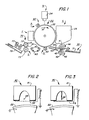
- FIG. 1 depicts schematically the various components thereof.
- like reference numerals will be employed throughout to designate identical elements.
- the apparatus of the present invention is disclosed as a means for charging a photosensitive member, it should be understood that the invention could be used in an electrophotographic environment as a pre-cleaning, transfer or detack device or any other apparatus in which uniform surface potential is desired or required.
- a drum 20 having a photoconductive surface 22 entrained about and secured to the exterior circumferential surface of a conductive substrate is rotated in the direction of arrow 10 through the various processing stations.
- photoconductive surface 22 may be made from selenium of the type described in U.S. Patent 2,970,906.
- a suitable conductive substrate is made from aluminum.
- drum 20 rotates a portion of photoconductive surface 22 through charging station A.
- Charging station A employs a corona generating device in accordance with the present invention, indicated generally by the reference numeral 80, to charge photoconductive surface 22 to a relatively high substantially uniform potential.
- Exposure station B includes an exposure mechanism, indicated generally by the reference numeral 24, having a stationary, transparent platen, such as a glass plate or the like for supporting an original document thereon. Lamps illuminate the original document. Scanning of the original document is achieved by oscillating a mirror in a timed relationship with the movement of drum 20 or by translating the lamps and lens across the original document so as to create incremental light images which are projected through an apertured slit onto the charged portion of photoconductive surface 22. Irradiation of the charged portion of photoconductive surface 22 records an electrostatic latent image corresponding to the information areas contained within the original document.
- Drum 20 rotates the electrostatic latent image recorded on photoconductive surface 22 to development station C.
- Development station C includes a developer unit, indicated generally by the reference numeral 25, having a housing with a supply of developer mix contained therein.
- the developer mix comprises carrier granules with toner particles adhering triboelectrically thereto.
- the carrier granules are formed from a magnetic material with the toner particles being made from a heat settable plastic.
- Developer unit 25 is preferably a magnetic brush development system. A system of this type moves the developer mix through a directional flux field to form a brush thereof.
- the electrostatic latent image recorded on photoconductive surface 22 is developed by bringing the brush of developer mix into contact therewith. In this manner, the toner particles are attracted electrostatically from the carrier granules to the latent image forming a toner powder image on photoconductive surface 22.
- a copy sheet is advanced by sheet feeding apparatus 30 to transfer station D.
- Sheet feed apparatus 30 advances successive copy sheets to forwarding registration rollers 40 and 41.
- Forwarding registration roller 40 is driven conventionally by a motor (not shown) in the direction of arrow 45 thereby also rotating idler roller 41 which is in contact therewith in the direction of arrow 46.
- feed device 30 operates to advance the uppermost substrate or sheet from stack 31 into registration rollers 40 and 41 and against registration fingers 42.
- Fingers 42 are actuated by conventional means in timed relation to an image on drum 20 such that the sheet resting against the fingers is forwarded toward the drum in synchronism with the image on the drum.
- a conventional registration finger control system is shown in U.S. Patent 3,902,715. After the sheet is released by finger 42, it is advanced through a chute formed by guides 43 and 44 to transfer station D.
- transfer station D also includes an efficient corona generating device 50 in accordance with the present invention which applies a spray of ions to the back side of the copy sheet. This attracts the toner powder image from photoconductive surface 22 to the copy sheet.
- the sheet After transfer of the toner powder image to the copy sheet, the sheet is advanced by endless belt conveyor 60, in the direction of arrow 61, to fusing station E.
- Fusing station E includes a fuser assembly indicated generally by the reference numeral 70.
- Fuser assembly 70 includes a fuser roll 72 and a backup roll 73 defining a nip therebetween through which the copy sheet passes. After the fusing process is completed, the copy sheet is advanced by conventional rollers 75 to catch tray 78.
- Cleaning station F includes a corona generating device (not shown) adapted to neutralize the remaining electrostatic charge on photo-conductive surface 22 and that of the residual toner particles.
- the neutralized toner particles are then cleaned from photoconductive surface 22 by a rotatably mounted fibrous brush (not shown) in contact therewith.
- a discharge lamp (not shown) floods photoconductive surface 22 with light to dissipate any residual electrostatic charge remaining thereon prior to the charging thereof for the next successive imaging cycle.
- Figure 2 depicts the corona generating device 80 in greater detail.
- the corona generating scorotron unit is positioned above the photosensitive surface 22 and is arranged to deposit an electrical charge thereon as the surface 22 moves in a clockwise direction.
- the corona unit 80 includes an insulating shield 81 which partially encircles a substantial portion of corona generating electrode 85 that preferably comprises a 37 ⁇ m wire mounted transverse to the direction of movement of photoreceptor 20.
- a control screen 82 encloses the corona emitting wire 85 and is spaced from photoreceptor surface 22.
- the corona electrode utilized in the present embodiment is connected to the negative terminal of the power source through a limiting resistor, whereby negative ion charges are placed on the photosensitive surface 22.
- an opposite polarity can be employed to obtain positive charge.
- Conventionally, as in U.S. Patent 2,836,725 corona generators have been designed with a cross sectional area of 6 cm2 and use thin wire (90 ⁇ m) located about 6mm from a shield surrounding the wire and about 12mm from the receiver surface. Large power supplies for high charging voltages of new 7kV with a 40 cm long wire are required for such devices in order to get a current of 88 ⁇ A or 2.2 ⁇ A/cm.
- scorotron devices i.e., corona generators with control screens positioned between the corona wire and receiver, the screens are spaced a great distance (e.g. 12mm) from the wire as well as the receiver surface.
- An advantage of the close spacings (see below) of the present device is being able to employ reduced high voltages ( ⁇ 5 kV).
- Thin wires 85 are employed, spaced from mesh screen 82 by about 3 to 5mm.
- This compact scorotron system is successful at charging photoreceptors uniformly at speeds up to 25 cm/sec for each wire or channel.
- electrometer measurements show -900 to -920 volts DC output range along a 25cm length scorotron.
- the final surface potential at all points along the receiver surface indicates a totally stable -920 volts, the applied grid voltage, for a 25cm/sec receiver speed.
- the device has the combination of a low radius corona emission surface, a tight screen for control (30 -80% open, but preferably 65% open), and small screen-to-receiver spacing with sufficient impedance to the coronode to prevent arcing.
- An insulating shield is also included with the aforementioned structure to provide uniform and efficient charging of a receiver surface.
- Screen 82 has a thickness of between 3 to 25 mils (75 - 635 ⁇ m) and preferably 3 to 5 mils (75 - 127 ⁇ m). It has been found that screen efficiency shows excellent inverse correlation with thickness.
- the low radius coronode with voltage control (scorotron) screen is placed close enough to photoreceptor 20 that fringing fields between screen 82 and photoreceptor surface 22 contribute to efficient ion pumping or flow as well as potential leveling on photoreceptor surface 22. It has been found that 1.5mm is a good trade-off between better "pumping action" (fringing fields) and critical spacing tolerances.
- This charging device is capable of AC charge or discharge and is ideal for color copying where a maximum charging speed can be compromised in order to obtain a very precise, uniform level of potential, and where tone reproduction makes charge uniformity even more critical.
- the scorotron device of the present invention is adapted to be highly efficient.
- the plastic non-conductive shield 81 allows ions from the high voltage coronode to go toward screen 82 which is at the desired charging potential of the photoreceptor surface 22.
- the ions from coronode 85 are not conducted by the shield but emitted toward the screen, instead.
- the ions are driven by more localized fringing fields through the holes of the screen and onto the photoreceptor surface.
- the fringing fields collapse and the field lines from the coronode terminate on the screen, thereby driving the ions to the screen and limiting the photoreceptor surface to that potential.
- the screen has a fixed voltage applied to it so the coronode can be kept above threshold due to the proximity and area of the biased screen; therefore a conductive shield is not necessary to maintain corona.
- a charging unit such as 80 that has a 12mm wide channel operated without change in coronode current, as an insulating shield was brought to within 6mm above the coronode wire, and with the wire spaced 3mm above the screen.
- an embodiment of the present invention is shown that comprises sawteeth 86 of Beryllium copper on 3mm centers.
- the sawteeth are spaced from mesh screen 83 by about 5mm.
- the spacing between the mesh screen and photoreceptor 22 is about 1.5mm.
- This embodiment substantially reduces ozone production when charging takes place.
- the sawteeth are enclosed in an insulating housing 81 and are energized by a conventional electrical potential source, as is screen 83.
- Voltage control screen 83 is positioned close enough to the receiver to produce fringing fields until the receiver potential reaches that of the screen, thereby providing high efficiency and good control of the potential on the photoreceptor surface.
Landscapes
- Physics & Mathematics (AREA)
- Engineering & Computer Science (AREA)
- Plasma & Fusion (AREA)
- General Physics & Mathematics (AREA)
- Electrostatic Charge, Transfer And Separation In Electrography (AREA)
Claims (7)
- Dispositif à scoroton pour appliquer une charge à une surface photoconductrice (22), le dispositif comprenant un écran (81), une électrode d'émission d'effet corona (85) placée à l'intérieur dudit écran et destinée à provoquer des émissions à effet couronne lorsqu'elle est mise sous tension; une alimentation destinée à fournir de l'énergie à ladite électrode; et un écran (82) placé entre ladite électrode et ladite surface photoconductrice, caractérisé en ce que l'écran est non conducteur; en ce que l'écran est ouvert entre 30 et 80 % et est séparé de l'électrode d'une distance comprise dans la plage allant de 3 à 5 mm et de la surface photoconductrice d'une distance comprise dans la plage allant de 1,5 à 2 mm; et en ce qu'un moyen d'impédance est connecté à l'électrode pour éviter la formation d'arcs.
- Dispositif selon la revendication 1, dans lequel ledit écran est ouvert à environ 65 %.
- Dispositif selon la revendication 1 ou la revendication 2, dans lequel ledit écran a une épaisseur comprise entre 75 et 635 µm et de préférence entre 75 et 127 µm.
- Dispositif selon l'une quelconque des revendications précédentes, caractérisé en ce que ladite électrode est séparée dudit écran de 4 - 5 mm.
- Dispositif selon l'une quelconque des revendications précédentes, dans lequel ladite électrode est au moins un fil de coronode.
- Dispositif selon l'une quelconque des revendications 1 à 4, dans lequel ladite électrode comprend une coronode en dents de scie.
- Dispositif selon l'une quelconque des revendications précédentes, comprenant un moyen pour appliquer un potentiel de commande à l'écran de sorte que des ions provenant de ladite électrode sont émis vers ledit écran et alors qu'ils se rapprochent du plan de l'écran sont entraînés par les champs de fuite par l'intermédiaire dudit écran pour tomber sur ladite surface photoconductrice, jusqu'à ce que le potentiel de la surface photoconductrice atteigne celui de l'écran.
Applications Claiming Priority (2)
| Application Number | Priority Date | Filing Date | Title |
|---|---|---|---|
| US06/567,717 US4591713A (en) | 1984-01-03 | 1984-01-03 | Efficient, self-limiting corona device for positive or negative charging |
| US567717 | 1984-01-03 |
Publications (3)
| Publication Number | Publication Date |
|---|---|
| EP0147985A2 EP0147985A2 (fr) | 1985-07-10 |
| EP0147985A3 EP0147985A3 (en) | 1987-07-01 |
| EP0147985B1 true EP0147985B1 (fr) | 1991-10-30 |
Family
ID=24268356
Family Applications (1)
| Application Number | Title | Priority Date | Filing Date |
|---|---|---|---|
| EP84308732A Expired EP0147985B1 (fr) | 1984-01-03 | 1984-12-14 | Dispositif de décharge corona |
Country Status (5)
| Country | Link |
|---|---|
| US (1) | US4591713A (fr) |
| EP (1) | EP0147985B1 (fr) |
| JP (1) | JPS60158582A (fr) |
| CA (1) | CA1235731A (fr) |
| DE (1) | DE3485226D1 (fr) |
Families Citing this family (23)
| Publication number | Priority date | Publication date | Assignee | Title |
|---|---|---|---|---|
| US4638397A (en) * | 1984-12-21 | 1987-01-20 | Xerox Corporation | Self-biased scorotron and control therefor |
| US4739363A (en) * | 1985-03-26 | 1988-04-19 | Canon Kabushiki Kaisha | Image forming apparatus |
| US4725731A (en) * | 1986-07-02 | 1988-02-16 | Xerox Corporation | Photoreceptor deletion control by utilization of corona wind |
| US4725732A (en) * | 1986-07-02 | 1988-02-16 | Xerox Corporation | Pin corotron and scorotron assembly |
| US4963738A (en) * | 1986-12-22 | 1990-10-16 | Xerox Corporation | Flat comb-like scorotron charging device |
| US4792680A (en) * | 1987-01-12 | 1988-12-20 | Xerox Corporation | Corona device having a beryllium copper screen |
| US4841146A (en) * | 1987-08-03 | 1989-06-20 | Xerox Corporation | Self-cleaning scorotron with focused ion beam |
| US4775915A (en) * | 1987-10-05 | 1988-10-04 | Eastman Kodak Company | Focussed corona charger |
| US4910400A (en) * | 1987-10-23 | 1990-03-20 | Eastman Kodak Company | Programmable focussed corona charger |
| US4868611A (en) * | 1987-12-10 | 1989-09-19 | Xerox Corporation | Highlight color imaging with first image neutralization using a scorotron |
| US4899186A (en) * | 1989-06-19 | 1990-02-06 | Xerox Corporation | Ionographic device with pin array coronode |
| US5105223A (en) * | 1991-05-01 | 1992-04-14 | Xerox Corporation | Screened blade scorotron |
| EP0810487B1 (fr) * | 1992-06-04 | 2000-01-05 | Sharp Kabushiki Kaisha | Chargeur |
| JP2810590B2 (ja) * | 1992-06-26 | 1998-10-15 | シャープ株式会社 | 帯電装置 |
| US6208499B1 (en) | 1993-07-12 | 2001-03-27 | Minolta Co., Ltd. | Corona discharge device |
| US5466938A (en) * | 1993-09-30 | 1995-11-14 | Minolta Co., Ltd. | Corona discharge device |
| WO1996013085A1 (fr) * | 1994-10-19 | 1996-05-02 | Haug Gmbh & Co. Kg | Dispositif pour l'application de charges electriques unipolaires |
| US5907468A (en) * | 1994-10-19 | 1999-05-25 | Haug Gmbh & Co. Kg | Device for applying unipolar electrical charges to a moving electrically-insulated surface using a corona electrode |
| CN100485542C (zh) * | 2006-02-13 | 2009-05-06 | 夏普株式会社 | 带电装置、图像形成装置 |
| US7647014B2 (en) * | 2006-02-13 | 2010-01-12 | Sharp Kabushiki Kaisha | Pretransfer charging device and image forming apparatus including same |
| JP2007241244A (ja) * | 2006-02-13 | 2007-09-20 | Sharp Corp | 帯電装置、画像形成装置、および帯電方法 |
| DE102007046610B4 (de) * | 2007-09-28 | 2009-06-10 | OCé PRINTING SYSTEMS GMBH | Vorrichtung zur Einstellung des elektrischen Potentials bei einem bewegten bandförmigen Träger aus halbleiterfähigem Material für Farbpartikel bei einem elektrografischen Druck- oder Kopiergerät |
| US20130343781A1 (en) * | 2012-06-20 | 2013-12-26 | Xerox Corporation | Titanium scorotron grid |
Family Cites Families (17)
| Publication number | Priority date | Publication date | Assignee | Title |
|---|---|---|---|---|
| US2588699A (en) * | 1943-08-27 | 1952-03-11 | Chester F Carlson | Electrophotographic apparatus |
| US2777957A (en) * | 1950-04-06 | 1957-01-15 | Haloid Co | Corona discharge device |
| US2970906A (en) * | 1955-08-05 | 1961-02-07 | Haloid Xerox Inc | Xerographic plate and a process of copy-making |
| US2836725A (en) * | 1956-11-19 | 1958-05-27 | Haloid Co | Corona charging device |
| US3396308A (en) * | 1965-07-02 | 1968-08-06 | Eastman Kodak Co | Web treating device |
| US3456109A (en) * | 1966-11-07 | 1969-07-15 | Addressograph Multigraph | Method and means for photoelectrostatic charging |
| US3691373A (en) * | 1970-04-20 | 1972-09-12 | First City National Bank Of Ho | Corona device |
| US3959690A (en) * | 1972-03-20 | 1976-05-25 | Hoechst Aktiengesellschaft | Corona discharge element |
| US3902715A (en) * | 1972-08-30 | 1975-09-02 | Xerox Corp | Sheet registration for paper handling apparatus |
| GB1451647A (fr) * | 1973-12-21 | 1976-10-06 | ||
| SE415300B (sv) * | 1975-07-14 | 1980-09-22 | Xerox Corp | Anordning for kronaurladdning |
| JPS5252641A (en) * | 1975-10-25 | 1977-04-27 | Mita Ind Co Ltd | Corona discharge device |
| JPS5343537A (en) * | 1976-10-01 | 1978-04-19 | Olympus Optical Co Ltd | Corona charger |
| US4156141A (en) * | 1978-01-16 | 1979-05-22 | Pitney-Bowes, Inc. | Corona wire damage control resistor |
| FR2415528A1 (fr) * | 1978-01-25 | 1979-08-24 | Cellophane Sa | Amelioration aux procedes de fabrication de films par placage electrostatique |
| JPS5577761A (en) * | 1978-12-07 | 1980-06-11 | Canon Inc | Corona discharger |
| US4322156A (en) * | 1979-08-14 | 1982-03-30 | Tokyo Shibaura Denki Kabushiki Kaisha | Charging apparatus for copying machine |
-
1984
- 1984-01-03 US US06/567,717 patent/US4591713A/en not_active Expired - Lifetime
- 1984-12-14 EP EP84308732A patent/EP0147985B1/fr not_active Expired
- 1984-12-14 DE DE8484308732T patent/DE3485226D1/de not_active Expired - Fee Related
- 1984-12-26 JP JP59282058A patent/JPS60158582A/ja active Pending
-
1985
- 1985-01-02 CA CA000471329A patent/CA1235731A/fr not_active Expired
Also Published As
| Publication number | Publication date |
|---|---|
| CA1235731A (fr) | 1988-04-26 |
| US4591713A (en) | 1986-05-27 |
| DE3485226D1 (de) | 1991-12-05 |
| JPS60158582A (ja) | 1985-08-19 |
| EP0147985A2 (fr) | 1985-07-10 |
| EP0147985A3 (en) | 1987-07-01 |
Similar Documents
| Publication | Publication Date | Title |
|---|---|---|
| EP0147985B1 (fr) | Dispositif de décharge corona | |
| US3496352A (en) | Self-cleaning corona generating apparatus | |
| US5585894A (en) | Process cartridge with a movable image bearing member as well as a contactable member, and an image forming apparatus having the same | |
| US3382360A (en) | Xerographic charging system having means for providing an air cushion between the charging device and the xerographic drum | |
| US3324291A (en) | Corona generating device with means to cause air flow therethrough to maintain the parts free of dust accumulation | |
| US3944356A (en) | Charging apparatus | |
| US2965756A (en) | Electrostatic charging apparatus | |
| US4697914A (en) | Toner containment method and apparatus | |
| JPS61100771A (ja) | 感光体荷電用スコロトロン | |
| US3611074A (en) | Corona discharge device | |
| US3794839A (en) | Corona generating apparatus | |
| CA1247694A (fr) | Dispositif de charge de coronode | |
| US4351603A (en) | Electronic copying apparatus | |
| IL31765A (en) | Method and device for the electrostatic charging of surfaces | |
| US4558221A (en) | Self limiting mini-corotron | |
| US4762997A (en) | Fluid jet assisted ion projection charging method | |
| CA1230915A (fr) | Methode et appareil d'electrophotographie | |
| US4248951A (en) | Method of image formation with a screen element and charging means | |
| US4105320A (en) | Transfer of conductive particles | |
| EP0147206A2 (fr) | Scorotron à enroulement corona segmenté | |
| US5563688A (en) | Charging device for charging in one of a plurality of predefined image areas on a surface of an imaging member | |
| US5729807A (en) | Optically switched commutator scheme for hybrid scavengeless segmented electroded donor rolls | |
| US5666601A (en) | Resistive ion source charging device | |
| US4448512A (en) | Light means for exposing and light means for discharging in a electrophotographic printing machine | |
| EP0816933B1 (fr) | Dispositif et procédé xérographique pour chargement et transfert |
Legal Events
| Date | Code | Title | Description |
|---|---|---|---|
| PUAI | Public reference made under article 153(3) epc to a published international application that has entered the european phase |
Free format text: ORIGINAL CODE: 0009012 |
|
| AK | Designated contracting states |
Designated state(s): DE FR GB |
|
| PUAL | Search report despatched |
Free format text: ORIGINAL CODE: 0009013 |
|
| AK | Designated contracting states |
Kind code of ref document: A3 Designated state(s): DE FR GB |
|
| 17P | Request for examination filed |
Effective date: 19871222 |
|
| 17Q | First examination report despatched |
Effective date: 19890505 |
|
| GRAA | (expected) grant |
Free format text: ORIGINAL CODE: 0009210 |
|
| AK | Designated contracting states |
Kind code of ref document: B1 Designated state(s): DE FR GB |
|
| REF | Corresponds to: |
Ref document number: 3485226 Country of ref document: DE Date of ref document: 19911205 |
|
| ET | Fr: translation filed | ||
| PLBE | No opposition filed within time limit |
Free format text: ORIGINAL CODE: 0009261 |
|
| STAA | Information on the status of an ep patent application or granted ep patent |
Free format text: STATUS: NO OPPOSITION FILED WITHIN TIME LIMIT |
|
| 26N | No opposition filed | ||
| PGFP | Annual fee paid to national office [announced via postgrant information from national office to epo] |
Ref country code: DE Payment date: 20001204 Year of fee payment: 17 |
|
| PGFP | Annual fee paid to national office [announced via postgrant information from national office to epo] |
Ref country code: FR Payment date: 20001212 Year of fee payment: 17 |
|
| PGFP | Annual fee paid to national office [announced via postgrant information from national office to epo] |
Ref country code: GB Payment date: 20001213 Year of fee payment: 17 |
|
| PG25 | Lapsed in a contracting state [announced via postgrant information from national office to epo] |
Ref country code: GB Free format text: LAPSE BECAUSE OF NON-PAYMENT OF DUE FEES Effective date: 20011214 |
|
| REG | Reference to a national code |
Ref country code: GB Ref legal event code: IF02 |
|
| PG25 | Lapsed in a contracting state [announced via postgrant information from national office to epo] |
Ref country code: DE Free format text: LAPSE BECAUSE OF NON-PAYMENT OF DUE FEES Effective date: 20020702 |
|
| GBPC | Gb: european patent ceased through non-payment of renewal fee |
Effective date: 20011214 |
|
| PG25 | Lapsed in a contracting state [announced via postgrant information from national office to epo] |
Ref country code: FR Free format text: LAPSE BECAUSE OF NON-PAYMENT OF DUE FEES Effective date: 20020830 |
|
| REG | Reference to a national code |
Ref country code: FR Ref legal event code: ST |