EP0147985B1 - Corona device - Google Patents
Corona device Download PDFInfo
- Publication number
- EP0147985B1 EP0147985B1 EP84308732A EP84308732A EP0147985B1 EP 0147985 B1 EP0147985 B1 EP 0147985B1 EP 84308732 A EP84308732 A EP 84308732A EP 84308732 A EP84308732 A EP 84308732A EP 0147985 B1 EP0147985 B1 EP 0147985B1
- Authority
- EP
- European Patent Office
- Prior art keywords
- screen
- electrode
- corona
- charging
- photoconductive surface
- Prior art date
- Legal status (The legal status is an assumption and is not a legal conclusion. Google has not performed a legal analysis and makes no representation as to the accuracy of the status listed.)
- Expired
Links
Images
Classifications
-
- G—PHYSICS
- G03—PHOTOGRAPHY; CINEMATOGRAPHY; ANALOGOUS TECHNIQUES USING WAVES OTHER THAN OPTICAL WAVES; ELECTROGRAPHY; HOLOGRAPHY
- G03G—ELECTROGRAPHY; ELECTROPHOTOGRAPHY; MAGNETOGRAPHY
- G03G15/00—Apparatus for electrographic processes using a charge pattern
- G03G15/02—Apparatus for electrographic processes using a charge pattern for laying down a uniform charge, e.g. for sensitising; Corona discharge devices
- G03G15/0291—Apparatus for electrographic processes using a charge pattern for laying down a uniform charge, e.g. for sensitising; Corona discharge devices corona discharge devices, e.g. wires, pointed electrodes, means for cleaning the corona discharge device
-
- H—ELECTRICITY
- H01—ELECTRIC ELEMENTS
- H01T—SPARK GAPS; OVERVOLTAGE ARRESTERS USING SPARK GAPS; SPARKING PLUGS; CORONA DEVICES; GENERATING IONS TO BE INTRODUCED INTO NON-ENCLOSED GASES
- H01T19/00—Devices providing for corona discharge
Definitions
- This invention relates to a corona device for charging a surface uniformly either positive or negative. More particularly, this invention relates to a scorotron charging device for charging photoreceptors.
- DE-A-2 948 972 describes in detail a corona discharging device for discharging the surface of an image bearing member.
- the device has two shield cases disposed side by side and at least one corona wire in each shield case. Grids are provided between the corona wires and the image bearing member, at a minimum spacing of about 1 mm from the latter to achieve increased charging speed.
- the present invention provides a scorotron device for applying a charge to a photoconductive surface, comprising: a shield; a corona-emitting electrode positioned within said shield and adapted to give off corona emissions when energized; a power source adapted to supply energy to said electrode; and a screen placed between said electrode and said photoconductive surface.
- the device is characterized in that the shield is non-conductive; in that the screen is between 30 and 80% open and is separated from the electrode by a distance within the range of from 3 to 5mm and from the photoconductive surface by a distance within the range of 1.5 to 2mm; and in that impedance means is connected to the electrode to prevent arcing.
- the impedance should be selected to provide about a 10% drop in potential from the power source to the electrode.
- the electrode is separated from the screen by 4 to 5mm.
- the present invention enables more uniform charging of photoreceptors, with greater efficiency and stability, lower manufacturing and service costs, and decreased production of ozone and nitrate by- products, especially for negative charging.
- FIG. 1 depicts schematically the various components thereof.
- like reference numerals will be employed throughout to designate identical elements.
- the apparatus of the present invention is disclosed as a means for charging a photosensitive member, it should be understood that the invention could be used in an electrophotographic environment as a pre-cleaning, transfer or detack device or any other apparatus in which uniform surface potential is desired or required.
- a drum 20 having a photoconductive surface 22 entrained about and secured to the exterior circumferential surface of a conductive substrate is rotated in the direction of arrow 10 through the various processing stations.
- photoconductive surface 22 may be made from selenium of the type described in U.S. Patent 2,970,906.
- a suitable conductive substrate is made from aluminum.
- drum 20 rotates a portion of photoconductive surface 22 through charging station A.
- Charging station A employs a corona generating device in accordance with the present invention, indicated generally by the reference numeral 80, to charge photoconductive surface 22 to a relatively high substantially uniform potential.
- Exposure station B includes an exposure mechanism, indicated generally by the reference numeral 24, having a stationary, transparent platen, such as a glass plate or the like for supporting an original document thereon. Lamps illuminate the original document. Scanning of the original document is achieved by oscillating a mirror in a timed relationship with the movement of drum 20 or by translating the lamps and lens across the original document so as to create incremental light images which are projected through an apertured slit onto the charged portion of photoconductive surface 22. Irradiation of the charged portion of photoconductive surface 22 records an electrostatic latent image corresponding to the information areas contained within the original document.
- Drum 20 rotates the electrostatic latent image recorded on photoconductive surface 22 to development station C.
- Development station C includes a developer unit, indicated generally by the reference numeral 25, having a housing with a supply of developer mix contained therein.
- the developer mix comprises carrier granules with toner particles adhering triboelectrically thereto.
- the carrier granules are formed from a magnetic material with the toner particles being made from a heat settable plastic.
- Developer unit 25 is preferably a magnetic brush development system. A system of this type moves the developer mix through a directional flux field to form a brush thereof.
- the electrostatic latent image recorded on photoconductive surface 22 is developed by bringing the brush of developer mix into contact therewith. In this manner, the toner particles are attracted electrostatically from the carrier granules to the latent image forming a toner powder image on photoconductive surface 22.
- a copy sheet is advanced by sheet feeding apparatus 30 to transfer station D.
- Sheet feed apparatus 30 advances successive copy sheets to forwarding registration rollers 40 and 41.
- Forwarding registration roller 40 is driven conventionally by a motor (not shown) in the direction of arrow 45 thereby also rotating idler roller 41 which is in contact therewith in the direction of arrow 46.
- feed device 30 operates to advance the uppermost substrate or sheet from stack 31 into registration rollers 40 and 41 and against registration fingers 42.
- Fingers 42 are actuated by conventional means in timed relation to an image on drum 20 such that the sheet resting against the fingers is forwarded toward the drum in synchronism with the image on the drum.
- a conventional registration finger control system is shown in U.S. Patent 3,902,715. After the sheet is released by finger 42, it is advanced through a chute formed by guides 43 and 44 to transfer station D.
- transfer station D also includes an efficient corona generating device 50 in accordance with the present invention which applies a spray of ions to the back side of the copy sheet. This attracts the toner powder image from photoconductive surface 22 to the copy sheet.
- the sheet After transfer of the toner powder image to the copy sheet, the sheet is advanced by endless belt conveyor 60, in the direction of arrow 61, to fusing station E.
- Fusing station E includes a fuser assembly indicated generally by the reference numeral 70.
- Fuser assembly 70 includes a fuser roll 72 and a backup roll 73 defining a nip therebetween through which the copy sheet passes. After the fusing process is completed, the copy sheet is advanced by conventional rollers 75 to catch tray 78.
- Cleaning station F includes a corona generating device (not shown) adapted to neutralize the remaining electrostatic charge on photo-conductive surface 22 and that of the residual toner particles.
- the neutralized toner particles are then cleaned from photoconductive surface 22 by a rotatably mounted fibrous brush (not shown) in contact therewith.
- a discharge lamp (not shown) floods photoconductive surface 22 with light to dissipate any residual electrostatic charge remaining thereon prior to the charging thereof for the next successive imaging cycle.
- Figure 2 depicts the corona generating device 80 in greater detail.
- the corona generating scorotron unit is positioned above the photosensitive surface 22 and is arranged to deposit an electrical charge thereon as the surface 22 moves in a clockwise direction.
- the corona unit 80 includes an insulating shield 81 which partially encircles a substantial portion of corona generating electrode 85 that preferably comprises a 37 ⁇ m wire mounted transverse to the direction of movement of photoreceptor 20.
- a control screen 82 encloses the corona emitting wire 85 and is spaced from photoreceptor surface 22.
- the corona electrode utilized in the present embodiment is connected to the negative terminal of the power source through a limiting resistor, whereby negative ion charges are placed on the photosensitive surface 22.
- an opposite polarity can be employed to obtain positive charge.
- Conventionally, as in U.S. Patent 2,836,725 corona generators have been designed with a cross sectional area of 6 cm2 and use thin wire (90 ⁇ m) located about 6mm from a shield surrounding the wire and about 12mm from the receiver surface. Large power supplies for high charging voltages of new 7kV with a 40 cm long wire are required for such devices in order to get a current of 88 ⁇ A or 2.2 ⁇ A/cm.
- scorotron devices i.e., corona generators with control screens positioned between the corona wire and receiver, the screens are spaced a great distance (e.g. 12mm) from the wire as well as the receiver surface.
- An advantage of the close spacings (see below) of the present device is being able to employ reduced high voltages ( ⁇ 5 kV).
- Thin wires 85 are employed, spaced from mesh screen 82 by about 3 to 5mm.
- This compact scorotron system is successful at charging photoreceptors uniformly at speeds up to 25 cm/sec for each wire or channel.
- electrometer measurements show -900 to -920 volts DC output range along a 25cm length scorotron.
- the final surface potential at all points along the receiver surface indicates a totally stable -920 volts, the applied grid voltage, for a 25cm/sec receiver speed.
- the device has the combination of a low radius corona emission surface, a tight screen for control (30 -80% open, but preferably 65% open), and small screen-to-receiver spacing with sufficient impedance to the coronode to prevent arcing.
- An insulating shield is also included with the aforementioned structure to provide uniform and efficient charging of a receiver surface.
- Screen 82 has a thickness of between 3 to 25 mils (75 - 635 ⁇ m) and preferably 3 to 5 mils (75 - 127 ⁇ m). It has been found that screen efficiency shows excellent inverse correlation with thickness.
- the low radius coronode with voltage control (scorotron) screen is placed close enough to photoreceptor 20 that fringing fields between screen 82 and photoreceptor surface 22 contribute to efficient ion pumping or flow as well as potential leveling on photoreceptor surface 22. It has been found that 1.5mm is a good trade-off between better "pumping action" (fringing fields) and critical spacing tolerances.
- This charging device is capable of AC charge or discharge and is ideal for color copying where a maximum charging speed can be compromised in order to obtain a very precise, uniform level of potential, and where tone reproduction makes charge uniformity even more critical.
- the scorotron device of the present invention is adapted to be highly efficient.
- the plastic non-conductive shield 81 allows ions from the high voltage coronode to go toward screen 82 which is at the desired charging potential of the photoreceptor surface 22.
- the ions from coronode 85 are not conducted by the shield but emitted toward the screen, instead.
- the ions are driven by more localized fringing fields through the holes of the screen and onto the photoreceptor surface.
- the fringing fields collapse and the field lines from the coronode terminate on the screen, thereby driving the ions to the screen and limiting the photoreceptor surface to that potential.
- the screen has a fixed voltage applied to it so the coronode can be kept above threshold due to the proximity and area of the biased screen; therefore a conductive shield is not necessary to maintain corona.
- a charging unit such as 80 that has a 12mm wide channel operated without change in coronode current, as an insulating shield was brought to within 6mm above the coronode wire, and with the wire spaced 3mm above the screen.
- an embodiment of the present invention is shown that comprises sawteeth 86 of Beryllium copper on 3mm centers.
- the sawteeth are spaced from mesh screen 83 by about 5mm.
- the spacing between the mesh screen and photoreceptor 22 is about 1.5mm.
- This embodiment substantially reduces ozone production when charging takes place.
- the sawteeth are enclosed in an insulating housing 81 and are energized by a conventional electrical potential source, as is screen 83.
- Voltage control screen 83 is positioned close enough to the receiver to produce fringing fields until the receiver potential reaches that of the screen, thereby providing high efficiency and good control of the potential on the photoreceptor surface.
Landscapes
- Physics & Mathematics (AREA)
- Engineering & Computer Science (AREA)
- Plasma & Fusion (AREA)
- General Physics & Mathematics (AREA)
- Electrostatic Charge, Transfer And Separation In Electrography (AREA)
Description
- This invention relates to a corona device for charging a surface uniformly either positive or negative. More particularly, this invention relates to a scorotron charging device for charging photoreceptors.
- Corona charging of xerographic photoreceptors has been disclosed in U.S. Patent 2,588,699. It has always been a problem that current levels for practical charging require coronode potentials of many thousands of volts, while photoreceptors typically cannot support more than 1000 volts surface potential without dielectric breakdown.
- One attempt at controlling the uniformity and magnitude of corona charging is U.S. Patent 2,777,957 which makes use of an open screen as a control electrode, to establish a reference potential, so that when the receiver surface reaches the screen voltage the fields no longer drive ions to the receiver, but rather to the screen. Unfortunately, a low porosity screen intercepts most of the ions, allowing a very small percentage to reach the intended receiver. A more open screen, on the other hand, delivers charge to the receiver more efficiently, but compromises the control function of the device.
- Further, problems with negative charging systems have historically been troublesome in charging a receptor uniformly. Some such systems involve the uses of wires, pins or sawteeth spaced at large distances from the receptor and thereby requiring high voltages. Charging units and power supplies, therefore, are relatively large and consume considerable space in, for example, a copying machine.
- Other methods exist for trying to obtain uniform charging from negative charging systems such as dicorotron charging devices as shown in U.S. Patent 4,086,650 that include glass coated wires and large specialized AC power supplies. A simpler system involves a screened corotron (scorotron). However, these methods are well known for being inefficient charging units, requiring slower charging speeds, and providing marginal uniformity.
- DE-A-2 948 972 describes in detail a corona discharging device for discharging the surface of an image bearing member. The device has two shield cases disposed side by side and at least one corona wire in each shield case. Grids are provided between the corona wires and the image bearing member, at a minimum spacing of about 1 mm from the latter to achieve increased charging speed.
- The present invention provides a scorotron device for applying a charge to a photoconductive surface, comprising: a shield; a corona-emitting electrode positioned within said shield and adapted to give off corona emissions when energized; a power source adapted to supply energy to said electrode; and a screen placed between said electrode and said photoconductive surface. The device is characterized in that the shield is non-conductive; in that the screen is between 30 and 80% open and is separated from the electrode by a distance within the range of from 3 to 5mm and from the photoconductive surface by a distance within the range of 1.5 to 2mm; and in that impedance means is connected to the electrode to prevent arcing.
- The impedance should be selected to provide about a 10% drop in potential from the power source to the electrode.
- Preferably, the electrode is separated from the screen by 4 to 5mm.
- The present invention enables more uniform charging of photoreceptors, with greater efficiency and stability, lower manufacturing and service costs, and decreased production of ozone and nitrate by- products, especially for negative charging.
- The foregoing and other features of the instant invention will be more apparent from a further reading of the specification and claims and from the following description with reference to drawings in which:
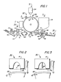
- Figure 1 is a schematic elevational view of an electrophotographic copying machine incorporating the features of the present invention.
- Figure 2 is an enlarged side view of an embodiment of the self limiting scorotron unit that comprises the present invention.
- Figure 3 is an enlarged side view of another embodiment of the self limiting scorotron unit of the present invention.
- While the invention will be described hereinafter in connection with a preferred embodiment, it will be understood that it is not intended to limit the invention to that embodiment.
- For a general understanding of an electrophotographic printing machine in which the features of the present invention may be incorporated, reference is made to Figure 1 which depicts schematically the various components thereof. Hereinafter, like reference numerals will be employed throughout to designate identical elements. Although the apparatus of the present invention is disclosed as a means for charging a photosensitive member, it should be understood that the invention could be used in an electrophotographic environment as a pre-cleaning, transfer or detack device or any other apparatus in which uniform surface potential is desired or required.
- Since the practice of electrophotographic copying is well known in the art, the various processing stations for producing a copy of an original document are represented in Figure 1 schematically. Each process station will be briefly described hereinafter.
- As in all electrophotographic copying machines of the type illustrated, a
drum 20 having aphotoconductive surface 22 entrained about and secured to the exterior circumferential surface of a conductive substrate is rotated in the direction of arrow 10 through the various processing stations. By way of example,photoconductive surface 22 may be made from selenium of the type described in U.S. Patent 2,970,906. A suitable conductive substrate is made from aluminum. - Initially,
drum 20 rotates a portion ofphotoconductive surface 22 through charging station A. Charging station A employs a corona generating device in accordance with the present invention, indicated generally by thereference numeral 80, to chargephotoconductive surface 22 to a relatively high substantially uniform potential. - Thereafter
drum 20 rotates the charged portion ofphotoconductive surface 22 to exposure station B. Exposure station B includes an exposure mechanism, indicated generally by thereference numeral 24, having a stationary, transparent platen, such as a glass plate or the like for supporting an original document thereon. Lamps illuminate the original document. Scanning of the original document is achieved by oscillating a mirror in a timed relationship with the movement ofdrum 20 or by translating the lamps and lens across the original document so as to create incremental light images which are projected through an apertured slit onto the charged portion ofphotoconductive surface 22. Irradiation of the charged portion ofphotoconductive surface 22 records an electrostatic latent image corresponding to the information areas contained within the original document. -
Drum 20 rotates the electrostatic latent image recorded onphotoconductive surface 22 to development station C. Development station C includes a developer unit, indicated generally by thereference numeral 25, having a housing with a supply of developer mix contained therein. The developer mix comprises carrier granules with toner particles adhering triboelectrically thereto. Preferably, the carrier granules are formed from a magnetic material with the toner particles being made from a heat settable plastic.Developer unit 25 is preferably a magnetic brush development system. A system of this type moves the developer mix through a directional flux field to form a brush thereof. The electrostatic latent image recorded onphotoconductive surface 22 is developed by bringing the brush of developer mix into contact therewith. In this manner, the toner particles are attracted electrostatically from the carrier granules to the latent image forming a toner powder image onphotoconductive surface 22. - With continued reference to Figure 1, a copy sheet is advanced by
sheet feeding apparatus 30 to transfer station D.Sheet feed apparatus 30 advances successive copy sheets to forwardingregistration rollers Forwarding registration roller 40 is driven conventionally by a motor (not shown) in the direction of arrow 45 thereby also rotatingidler roller 41 which is in contact therewith in the direction ofarrow 46. In operation,feed device 30 operates to advance the uppermost substrate or sheet from stack 31 intoregistration rollers registration fingers 42.Fingers 42 are actuated by conventional means in timed relation to an image ondrum 20 such that the sheet resting against the fingers is forwarded toward the drum in synchronism with the image on the drum. A conventional registration finger control system is shown in U.S. Patent 3,902,715. After the sheet is released byfinger 42, it is advanced through a chute formed byguides 43 and 44 to transfer station D. - Continuing now with the various processing stations, transfer station D also includes an efficient
corona generating device 50 in accordance with the present invention which applies a spray of ions to the back side of the copy sheet. This attracts the toner powder image fromphotoconductive surface 22 to the copy sheet. - After transfer of the toner powder image to the copy sheet, the sheet is advanced by
endless belt conveyor 60, in the direction of arrow 61, to fusing station E. - Fusing station E includes a fuser assembly indicated generally by the
reference numeral 70.Fuser assembly 70 includes afuser roll 72 and abackup roll 73 defining a nip therebetween through which the copy sheet passes. After the fusing process is completed, the copy sheet is advanced byconventional rollers 75 to catchtray 78. - Invariably, after the copy sheet is separated from
photoconductive surface 22, some residual toner particles remain adhering thereto. Those toner particles are removed fromphotoconductive surface 22 at cleaning station F. Cleaning station F includes a corona generating device (not shown) adapted to neutralize the remaining electrostatic charge on photo-conductive surface 22 and that of the residual toner particles. The neutralized toner particles are then cleaned fromphotoconductive surface 22 by a rotatably mounted fibrous brush (not shown) in contact therewith. Subsequent to cleaning, a discharge lamp (not shown) floodsphotoconductive surface 22 with light to dissipate any residual electrostatic charge remaining thereon prior to the charging thereof for the next successive imaging cycle. - It is believed that the foregoing description is sufficient for purposes of the present application to illustrate the general operation of an electrophotographic copying machine. Referring now to the subject matter of the present invention, Figure 2 depicts the corona generating
device 80 in greater detail. - Referring specifically to Figure 2, the detailed structure and operation of an aspect of the present invention will be described. The corona generating scorotron unit, generally referred to as 80, is positioned above the
photosensitive surface 22 and is arranged to deposit an electrical charge thereon as thesurface 22 moves in a clockwise direction. Thecorona unit 80 includes an insulating shield 81 which partially encircles a substantial portion ofcorona generating electrode 85 that preferably comprises a 37 µm wire mounted transverse to the direction of movement ofphotoreceptor 20. Acontrol screen 82 encloses thecorona emitting wire 85 and is spaced fromphotoreceptor surface 22. The corona electrode utilized in the present embodiment is connected to the negative terminal of the power source through a limiting resistor, whereby negative ion charges are placed on thephotosensitive surface 22. However, it should be clear that an opposite polarity can be employed to obtain positive charge. Conventionally, as in U.S. Patent 2,836,725 corona generators have been designed with a cross sectional area of 6 cm² and use thin wire (90 µm) located about 6mm from a shield surrounding the wire and about 12mm from the receiver surface. Large power supplies for high charging voltages of new 7kV with a 40 cm long wire are required for such devices in order to get a current of 88 µA or 2.2 µA/cm. In prior art scorotron devices, i.e., corona generators with control screens positioned between the corona wire and receiver, the screens are spaced a great distance (e.g. 12mm) from the wire as well as the receiver surface. - An advantage of the close spacings (see below) of the present device is being able to employ reduced high voltages (≃5 kV).
Thin wires 85 are employed, spaced frommesh screen 82 by about 3 to 5mm. This compact scorotron system is successful at charging photoreceptors uniformly at speeds up to 25 cm/sec for each wire or channel. With 1.5 mm between the receiver and screen, electrometer measurements show -900 to -920 volts DC output range along a 25cm length scorotron. The final surface potential at all points along the receiver surface indicates a totally stable -920 volts, the applied grid voltage, for a 25cm/sec receiver speed. The device has the combination of a low radius corona emission surface, a tight screen for control (30 -80% open, but preferably 65% open), and small screen-to-receiver spacing with sufficient impedance to the coronode to prevent arcing. An insulating shield is also included with the aforementioned structure to provide uniform and efficient charging of a receiver surface.Screen 82 has a thickness of between 3 to 25 mils (75 - 635µm) and preferably 3 to 5 mils (75 - 127µm). It has been found that screen efficiency shows excellent inverse correlation with thickness. - The low radius coronode with voltage control (scorotron) screen is placed close enough to photoreceptor 20 that fringing fields between
screen 82 andphotoreceptor surface 22 contribute to efficient ion pumping or flow as well as potential leveling onphotoreceptor surface 22. It has been found that 1.5mm is a good trade-off between better "pumping action" (fringing fields) and critical spacing tolerances. This charging device is capable of AC charge or discharge and is ideal for color copying where a maximum charging speed can be compromised in order to obtain a very precise, uniform level of potential, and where tone reproduction makes charge uniformity even more critical. - The scorotron device of the present invention is adapted to be highly efficient. The plastic non-conductive shield 81 allows ions from the high voltage coronode to go toward
screen 82 which is at the desired charging potential of thephotoreceptor surface 22. As a result, the ions fromcoronode 85 are not conducted by the shield but emitted toward the screen, instead. As they approach the plane of the screen, the ions are driven by more localized fringing fields through the holes of the screen and onto the photoreceptor surface. As the potential of the photoreceptor surface builds up to the voltage applied to the screen, the fringing fields collapse and the field lines from the coronode terminate on the screen, thereby driving the ions to the screen and limiting the photoreceptor surface to that potential. This gives an efficiency of between 30 - 50% and at times up to 80%. Using this scorotron system with positive charging is considered within the scope of the present invention, although it is not as essential in most positive charging applications, since corona emission from positive wire coronodes tends to be more uniform by nature. In the past, the relatively large scorotron units have employed a high percentage of open areas within the screen. Conductive shields were required because of the large spacing and high percentage openings, to keep the corona wires above threshold. However, withcorona generator 80 the coronode is separated from a 65% open screen by approximately 3mm. The screen has a fixed voltage applied to it so the coronode can be kept above threshold due to the proximity and area of the biased screen; therefore a conductive shield is not necessary to maintain corona. For example, a charging unit such as 80 that has a 12mm wide channel operated without change in coronode current, as an insulating shield was brought to within 6mm above the coronode wire, and with the wire spaced 3mm above the screen. - In Figure 3, an embodiment of the present invention is shown that comprises
sawteeth 86 of Beryllium copper on 3mm centers. The sawteeth are spaced frommesh screen 83 by about 5mm. The spacing between the mesh screen andphotoreceptor 22 is about 1.5mm. This embodiment substantially reduces ozone production when charging takes place. The sawteeth are enclosed in an insulating housing 81 and are energized by a conventional electrical potential source, as isscreen 83.Voltage control screen 83 is positioned close enough to the receiver to produce fringing fields until the receiver potential reaches that of the screen, thereby providing high efficiency and good control of the potential on the photoreceptor surface. - While the invention has been described with reference to the structure herein disclosed, it is not confined to the details as set forth and is intended to cover any modifications and changes that may come within the scope of the following claims.
Claims (7)
- A scorotron device for applying a charge to a photoconductive surface (22), the device comprising a shield (81); a corona-emitting electrode (85) positioned within said shield and adapted to give off corona emissions when energized; a power source adapted to supply energy to said electrode; and a screen (82) placed between said electrode and said photoconductive surface, characterized in that the shield is non-conductive; in that the screen is between 30 and 80% open and is separated from the electrode by a distance within the range of from 3 to 5mm and from the photoconductive surface by a distance within the range of 1.5 to 2mm; and in that impedance means is connected to the electrode to prevent arcing.
- A device as claimed in claim 1, wherein said screen is about 65% open.
- A device as claimed in claim 1 or claim 2, wherein said screen has a thickness of between 75 - 635µm (3 -25 mils) and preferably between 75 - 127µm (3 - 5 mils).
- A device as claimed in any one of the preceding claims, wherein said electrode is separated from said screen by 4 - 5mm.
- A device a claimed in any one of the preceding claims, wherein said electrode is at least one coronode wire.
- A device as claimed in any one of claims 1 to 4, wherein said electrode comprises a sawtooth coronode.
- A device as claimed in any one of the preceding claims, including means for applying a control potential to the screen so that ions from said electrode are emitted toward said screen and as they approach the plane of the screen are driven by fringing fields through said screen and onto said photoconductive surface, until the potential of the photoconductive surface reaches that of the screen.
Applications Claiming Priority (2)
| Application Number | Priority Date | Filing Date | Title |
|---|---|---|---|
| US06/567,717 US4591713A (en) | 1984-01-03 | 1984-01-03 | Efficient, self-limiting corona device for positive or negative charging |
| US567717 | 2000-05-10 |
Publications (3)
| Publication Number | Publication Date |
|---|---|
| EP0147985A2 EP0147985A2 (en) | 1985-07-10 |
| EP0147985A3 EP0147985A3 (en) | 1987-07-01 |
| EP0147985B1 true EP0147985B1 (en) | 1991-10-30 |
Family
ID=24268356
Family Applications (1)
| Application Number | Title | Priority Date | Filing Date |
|---|---|---|---|
| EP84308732A Expired EP0147985B1 (en) | 1984-01-03 | 1984-12-14 | Corona device |
Country Status (5)
| Country | Link |
|---|---|
| US (1) | US4591713A (en) |
| EP (1) | EP0147985B1 (en) |
| JP (1) | JPS60158582A (en) |
| CA (1) | CA1235731A (en) |
| DE (1) | DE3485226D1 (en) |
Families Citing this family (23)
| Publication number | Priority date | Publication date | Assignee | Title |
|---|---|---|---|---|
| US4638397A (en) * | 1984-12-21 | 1987-01-20 | Xerox Corporation | Self-biased scorotron and control therefor |
| US4739363A (en) * | 1985-03-26 | 1988-04-19 | Canon Kabushiki Kaisha | Image forming apparatus |
| US4725731A (en) * | 1986-07-02 | 1988-02-16 | Xerox Corporation | Photoreceptor deletion control by utilization of corona wind |
| US4725732A (en) * | 1986-07-02 | 1988-02-16 | Xerox Corporation | Pin corotron and scorotron assembly |
| US4963738A (en) * | 1986-12-22 | 1990-10-16 | Xerox Corporation | Flat comb-like scorotron charging device |
| US4792680A (en) * | 1987-01-12 | 1988-12-20 | Xerox Corporation | Corona device having a beryllium copper screen |
| US4841146A (en) * | 1987-08-03 | 1989-06-20 | Xerox Corporation | Self-cleaning scorotron with focused ion beam |
| US4775915A (en) * | 1987-10-05 | 1988-10-04 | Eastman Kodak Company | Focussed corona charger |
| US4910400A (en) * | 1987-10-23 | 1990-03-20 | Eastman Kodak Company | Programmable focussed corona charger |
| US4868611A (en) * | 1987-12-10 | 1989-09-19 | Xerox Corporation | Highlight color imaging with first image neutralization using a scorotron |
| US4899186A (en) * | 1989-06-19 | 1990-02-06 | Xerox Corporation | Ionographic device with pin array coronode |
| US5105223A (en) * | 1991-05-01 | 1992-04-14 | Xerox Corporation | Screened blade scorotron |
| EP0573758B1 (en) * | 1992-06-04 | 1998-02-25 | Sharp Kabushiki Kaisha | Charger |
| JP2810590B2 (en) * | 1992-06-26 | 1998-10-15 | シャープ株式会社 | Charging device |
| US6208499B1 (en) | 1993-07-12 | 2001-03-27 | Minolta Co., Ltd. | Corona discharge device |
| US5466938A (en) * | 1993-09-30 | 1995-11-14 | Minolta Co., Ltd. | Corona discharge device |
| WO1996013085A1 (en) * | 1994-10-19 | 1996-05-02 | Haug Gmbh & Co. Kg | Device for applying unipolar electrical charges |
| US5907468A (en) * | 1994-10-19 | 1999-05-25 | Haug Gmbh & Co. Kg | Device for applying unipolar electrical charges to a moving electrically-insulated surface using a corona electrode |
| US7647014B2 (en) * | 2006-02-13 | 2010-01-12 | Sharp Kabushiki Kaisha | Pretransfer charging device and image forming apparatus including same |
| CN100485542C (en) * | 2006-02-13 | 2009-05-06 | 夏普株式会社 | Charged device and image forming device |
| JP2007241244A (en) * | 2006-02-13 | 2007-09-20 | Sharp Corp | Charging device, image forming apparatus, and charging method |
| DE102007046610B4 (en) * | 2007-09-28 | 2009-06-10 | OCé PRINTING SYSTEMS GMBH | Device for adjusting the electric potential in a moving band-shaped carrier of semiconductor material for color particles in an electrographic printing or copying machine |
| US20130343781A1 (en) * | 2012-06-20 | 2013-12-26 | Xerox Corporation | Titanium scorotron grid |
Family Cites Families (17)
| Publication number | Priority date | Publication date | Assignee | Title |
|---|---|---|---|---|
| US2588699A (en) * | 1943-08-27 | 1952-03-11 | Chester F Carlson | Electrophotographic apparatus |
| US2777957A (en) * | 1950-04-06 | 1957-01-15 | Haloid Co | Corona discharge device |
| US2970906A (en) * | 1955-08-05 | 1961-02-07 | Haloid Xerox Inc | Xerographic plate and a process of copy-making |
| US2836725A (en) * | 1956-11-19 | 1958-05-27 | Haloid Co | Corona charging device |
| US3396308A (en) * | 1965-07-02 | 1968-08-06 | Eastman Kodak Co | Web treating device |
| US3456109A (en) * | 1966-11-07 | 1969-07-15 | Addressograph Multigraph | Method and means for photoelectrostatic charging |
| US3691373A (en) * | 1970-04-20 | 1972-09-12 | First City National Bank Of Ho | Corona device |
| US3959690A (en) * | 1972-03-20 | 1976-05-25 | Hoechst Aktiengesellschaft | Corona discharge element |
| US3902715A (en) * | 1972-08-30 | 1975-09-02 | Xerox Corp | Sheet registration for paper handling apparatus |
| GB1451647A (en) * | 1973-12-21 | 1976-10-06 | ||
| GB1554266A (en) * | 1975-07-14 | 1979-10-17 | Xerox Corp | Corona charging device |
| JPS5252641A (en) * | 1975-10-25 | 1977-04-27 | Mita Ind Co Ltd | Corona discharge device |
| JPS5343537A (en) * | 1976-10-01 | 1978-04-19 | Olympus Optical Co Ltd | Corona charger |
| US4156141A (en) * | 1978-01-16 | 1979-05-22 | Pitney-Bowes, Inc. | Corona wire damage control resistor |
| FR2415528A1 (en) * | 1978-01-25 | 1979-08-24 | Cellophane Sa | IMPROVEMENT OF THE MANUFACTURING PROCESSES OF FILMS BY ELECTROSTATIC PLATING |
| JPS5577761A (en) * | 1978-12-07 | 1980-06-11 | Canon Inc | Corona discharger |
| US4322156A (en) * | 1979-08-14 | 1982-03-30 | Tokyo Shibaura Denki Kabushiki Kaisha | Charging apparatus for copying machine |
-
1984
- 1984-01-03 US US06/567,717 patent/US4591713A/en not_active Expired - Lifetime
- 1984-12-14 EP EP84308732A patent/EP0147985B1/en not_active Expired
- 1984-12-14 DE DE8484308732T patent/DE3485226D1/en not_active Expired - Fee Related
- 1984-12-26 JP JP59282058A patent/JPS60158582A/en active Pending
-
1985
- 1985-01-02 CA CA000471329A patent/CA1235731A/en not_active Expired
Also Published As
| Publication number | Publication date |
|---|---|
| EP0147985A2 (en) | 1985-07-10 |
| JPS60158582A (en) | 1985-08-19 |
| US4591713A (en) | 1986-05-27 |
| DE3485226D1 (en) | 1991-12-05 |
| CA1235731A (en) | 1988-04-26 |
| EP0147985A3 (en) | 1987-07-01 |
Similar Documents
| Publication | Publication Date | Title |
|---|---|---|
| EP0147985B1 (en) | Corona device | |
| US3496352A (en) | Self-cleaning corona generating apparatus | |
| US3382360A (en) | Xerographic charging system having means for providing an air cushion between the charging device and the xerographic drum | |
| US3324291A (en) | Corona generating device with means to cause air flow therethrough to maintain the parts free of dust accumulation | |
| US3944356A (en) | Charging apparatus | |
| US2965756A (en) | Electrostatic charging apparatus | |
| US4697914A (en) | Toner containment method and apparatus | |
| JPS61100771A (en) | Scorotron for charging photosensitive substance | |
| US3611074A (en) | Corona discharge device | |
| US3794839A (en) | Corona generating apparatus | |
| CA1247694A (en) | Corona charging device | |
| US4351603A (en) | Electronic copying apparatus | |
| US4533230A (en) | Pin charging device for use in xerography | |
| IL31765A (en) | Method and device for the electrostatic charging of surfaces | |
| US4558221A (en) | Self limiting mini-corotron | |
| US4762997A (en) | Fluid jet assisted ion projection charging method | |
| CA1230915A (en) | Method and apparatus of electrophotography | |
| US4248951A (en) | Method of image formation with a screen element and charging means | |
| US4105320A (en) | Transfer of conductive particles | |
| EP0147206A2 (en) | Segmented coronode scorotron | |
| US5563688A (en) | Charging device for charging in one of a plurality of predefined image areas on a surface of an imaging member | |
| US5666601A (en) | Resistive ion source charging device | |
| US4448512A (en) | Light means for exposing and light means for discharging in a electrophotographic printing machine | |
| EP0816933B1 (en) | Xerographic device and method of charging and transfer | |
| US3945725A (en) | Flat screen electrostatic copier |
Legal Events
| Date | Code | Title | Description |
|---|---|---|---|
| PUAI | Public reference made under article 153(3) epc to a published international application that has entered the european phase |
Free format text: ORIGINAL CODE: 0009012 |
|
| AK | Designated contracting states |
Designated state(s): DE FR GB |
|
| PUAL | Search report despatched |
Free format text: ORIGINAL CODE: 0009013 |
|
| AK | Designated contracting states |
Kind code of ref document: A3 Designated state(s): DE FR GB |
|
| 17P | Request for examination filed |
Effective date: 19871222 |
|
| 17Q | First examination report despatched |
Effective date: 19890505 |
|
| GRAA | (expected) grant |
Free format text: ORIGINAL CODE: 0009210 |
|
| AK | Designated contracting states |
Kind code of ref document: B1 Designated state(s): DE FR GB |
|
| REF | Corresponds to: |
Ref document number: 3485226 Country of ref document: DE Date of ref document: 19911205 |
|
| ET | Fr: translation filed | ||
| PLBE | No opposition filed within time limit |
Free format text: ORIGINAL CODE: 0009261 |
|
| STAA | Information on the status of an ep patent application or granted ep patent |
Free format text: STATUS: NO OPPOSITION FILED WITHIN TIME LIMIT |
|
| 26N | No opposition filed | ||
| PGFP | Annual fee paid to national office [announced via postgrant information from national office to epo] |
Ref country code: DE Payment date: 20001204 Year of fee payment: 17 |
|
| PGFP | Annual fee paid to national office [announced via postgrant information from national office to epo] |
Ref country code: FR Payment date: 20001212 Year of fee payment: 17 |
|
| PGFP | Annual fee paid to national office [announced via postgrant information from national office to epo] |
Ref country code: GB Payment date: 20001213 Year of fee payment: 17 |
|
| PG25 | Lapsed in a contracting state [announced via postgrant information from national office to epo] |
Ref country code: GB Free format text: LAPSE BECAUSE OF NON-PAYMENT OF DUE FEES Effective date: 20011214 |
|
| REG | Reference to a national code |
Ref country code: GB Ref legal event code: IF02 |
|
| PG25 | Lapsed in a contracting state [announced via postgrant information from national office to epo] |
Ref country code: DE Free format text: LAPSE BECAUSE OF NON-PAYMENT OF DUE FEES Effective date: 20020702 |
|
| GBPC | Gb: european patent ceased through non-payment of renewal fee |
Effective date: 20011214 |
|
| PG25 | Lapsed in a contracting state [announced via postgrant information from national office to epo] |
Ref country code: FR Free format text: LAPSE BECAUSE OF NON-PAYMENT OF DUE FEES Effective date: 20020830 |
|
| REG | Reference to a national code |
Ref country code: FR Ref legal event code: ST |