EP0146197A2 - Removal of semiconductor wafers from dicing film - Google Patents
Removal of semiconductor wafers from dicing film Download PDFInfo
- Publication number
- EP0146197A2 EP0146197A2 EP84201904A EP84201904A EP0146197A2 EP 0146197 A2 EP0146197 A2 EP 0146197A2 EP 84201904 A EP84201904 A EP 84201904A EP 84201904 A EP84201904 A EP 84201904A EP 0146197 A2 EP0146197 A2 EP 0146197A2
- Authority
- EP
- European Patent Office
- Prior art keywords
- adhesive
- film
- support film
- wafer
- microns
- Prior art date
- Legal status (The legal status is an assumption and is not a legal conclusion. Google has not performed a legal analysis and makes no representation as to the accuracy of the status listed.)
- Withdrawn
Links
Images

Classifications
-
- H—ELECTRICITY
- H01—ELECTRIC ELEMENTS
- H01L—SEMICONDUCTOR DEVICES NOT COVERED BY CLASS H10
- H01L21/00—Processes or apparatus adapted for the manufacture or treatment of semiconductor or solid state devices or of parts thereof
- H01L21/67—Apparatus specially adapted for handling semiconductor or electric solid state devices during manufacture or treatment thereof; Apparatus specially adapted for handling wafers during manufacture or treatment of semiconductor or electric solid state devices or components ; Apparatus not specifically provided for elsewhere
- H01L21/67005—Apparatus not specifically provided for elsewhere
- H01L21/67011—Apparatus for manufacture or treatment
- H01L21/67132—Apparatus for placing on an insulating substrate, e.g. tape
-
- H—ELECTRICITY
- H01—ELECTRIC ELEMENTS
- H01L—SEMICONDUCTOR DEVICES NOT COVERED BY CLASS H10
- H01L21/00—Processes or apparatus adapted for the manufacture or treatment of semiconductor or solid state devices or of parts thereof
- H01L21/02—Manufacture or treatment of semiconductor devices or of parts thereof
- H01L21/04—Manufacture or treatment of semiconductor devices or of parts thereof the devices having at least one potential-jump barrier or surface barrier, e.g. PN junction, depletion layer or carrier concentration layer
- H01L21/18—Manufacture or treatment of semiconductor devices or of parts thereof the devices having at least one potential-jump barrier or surface barrier, e.g. PN junction, depletion layer or carrier concentration layer the devices having semiconductor bodies comprising elements of Group IV of the Periodic System or AIIIBV compounds with or without impurities, e.g. doping materials
- H01L21/28—Manufacture of electrodes on semiconductor bodies using processes or apparatus not provided for in groups H01L21/20 - H01L21/268
- H01L21/283—Deposition of conductive or insulating materials for electrodes conducting electric current
- H01L21/288—Deposition of conductive or insulating materials for electrodes conducting electric current from a liquid, e.g. electrolytic deposition
-
- B—PERFORMING OPERATIONS; TRANSPORTING
- B28—WORKING CEMENT, CLAY, OR STONE
- B28D—WORKING STONE OR STONE-LIKE MATERIALS
- B28D5/00—Fine working of gems, jewels, crystals, e.g. of semiconductor material; apparatus or devices therefor
- B28D5/0058—Accessories specially adapted for use with machines for fine working of gems, jewels, crystals, e.g. of semiconductor material
- B28D5/0082—Accessories specially adapted for use with machines for fine working of gems, jewels, crystals, e.g. of semiconductor material for supporting, holding, feeding, conveying or discharging work
-
- H—ELECTRICITY
- H01—ELECTRIC ELEMENTS
- H01L—SEMICONDUCTOR DEVICES NOT COVERED BY CLASS H10
- H01L21/00—Processes or apparatus adapted for the manufacture or treatment of semiconductor or solid state devices or of parts thereof
- H01L21/02—Manufacture or treatment of semiconductor devices or of parts thereof
- H01L21/04—Manufacture or treatment of semiconductor devices or of parts thereof the devices having at least one potential-jump barrier or surface barrier, e.g. PN junction, depletion layer or carrier concentration layer
- H01L21/18—Manufacture or treatment of semiconductor devices or of parts thereof the devices having at least one potential-jump barrier or surface barrier, e.g. PN junction, depletion layer or carrier concentration layer the devices having semiconductor bodies comprising elements of Group IV of the Periodic System or AIIIBV compounds with or without impurities, e.g. doping materials
- H01L21/30—Treatment of semiconductor bodies using processes or apparatus not provided for in groups H01L21/20 - H01L21/26
- H01L21/302—Treatment of semiconductor bodies using processes or apparatus not provided for in groups H01L21/20 - H01L21/26 to change their surface-physical characteristics or shape, e.g. etching, polishing, cutting
-
- H—ELECTRICITY
- H01—ELECTRIC ELEMENTS
- H01L—SEMICONDUCTOR DEVICES NOT COVERED BY CLASS H10
- H01L21/00—Processes or apparatus adapted for the manufacture or treatment of semiconductor or solid state devices or of parts thereof
- H01L21/67—Apparatus specially adapted for handling semiconductor or electric solid state devices during manufacture or treatment thereof; Apparatus specially adapted for handling wafers during manufacture or treatment of semiconductor or electric solid state devices or components ; Apparatus not specifically provided for elsewhere
- H01L21/68—Apparatus specially adapted for handling semiconductor or electric solid state devices during manufacture or treatment thereof; Apparatus specially adapted for handling wafers during manufacture or treatment of semiconductor or electric solid state devices or components ; Apparatus not specifically provided for elsewhere for positioning, orientation or alignment
-
- H—ELECTRICITY
- H01—ELECTRIC ELEMENTS
- H01L—SEMICONDUCTOR DEVICES NOT COVERED BY CLASS H10
- H01L21/00—Processes or apparatus adapted for the manufacture or treatment of semiconductor or solid state devices or of parts thereof
- H01L21/67—Apparatus specially adapted for handling semiconductor or electric solid state devices during manufacture or treatment thereof; Apparatus specially adapted for handling wafers during manufacture or treatment of semiconductor or electric solid state devices or components ; Apparatus not specifically provided for elsewhere
- H01L21/683—Apparatus specially adapted for handling semiconductor or electric solid state devices during manufacture or treatment thereof; Apparatus specially adapted for handling wafers during manufacture or treatment of semiconductor or electric solid state devices or components ; Apparatus not specifically provided for elsewhere for supporting or gripping
- H01L21/6835—Apparatus specially adapted for handling semiconductor or electric solid state devices during manufacture or treatment thereof; Apparatus specially adapted for handling wafers during manufacture or treatment of semiconductor or electric solid state devices or components ; Apparatus not specifically provided for elsewhere for supporting or gripping using temporarily an auxiliary support
- H01L21/6836—Wafer tapes, e.g. grinding or dicing support tapes
-
- H—ELECTRICITY
- H01—ELECTRIC ELEMENTS
- H01L—SEMICONDUCTOR DEVICES NOT COVERED BY CLASS H10
- H01L23/00—Details of semiconductor or other solid state devices
- H01L23/544—Marks applied to semiconductor devices or parts, e.g. registration marks, alignment structures, wafer maps
-
- H—ELECTRICITY
- H01—ELECTRIC ELEMENTS
- H01L—SEMICONDUCTOR DEVICES NOT COVERED BY CLASS H10
- H01L2221/00—Processes or apparatus adapted for the manufacture or treatment of semiconductor or solid state devices or of parts thereof covered by H01L21/00
- H01L2221/67—Apparatus for handling semiconductor or electric solid state devices during manufacture or treatment thereof; Apparatus for handling wafers during manufacture or treatment of semiconductor or electric solid state devices or components; Apparatus not specifically provided for elsewhere
- H01L2221/683—Apparatus for handling semiconductor or electric solid state devices during manufacture or treatment thereof; Apparatus for handling wafers during manufacture or treatment of semiconductor or electric solid state devices or components; Apparatus not specifically provided for elsewhere for supporting or gripping
- H01L2221/68304—Apparatus for handling semiconductor or electric solid state devices during manufacture or treatment thereof; Apparatus for handling wafers during manufacture or treatment of semiconductor or electric solid state devices or components; Apparatus not specifically provided for elsewhere for supporting or gripping using temporarily an auxiliary support
- H01L2221/68327—Apparatus for handling semiconductor or electric solid state devices during manufacture or treatment thereof; Apparatus for handling wafers during manufacture or treatment of semiconductor or electric solid state devices or components; Apparatus not specifically provided for elsewhere for supporting or gripping using temporarily an auxiliary support used during dicing or grinding
-
- H—ELECTRICITY
- H01—ELECTRIC ELEMENTS
- H01L—SEMICONDUCTOR DEVICES NOT COVERED BY CLASS H10
- H01L2924/00—Indexing scheme for arrangements or methods for connecting or disconnecting semiconductor or solid-state bodies as covered by H01L24/00
- H01L2924/0001—Technical content checked by a classifier
- H01L2924/0002—Not covered by any one of groups H01L24/00, H01L24/00 and H01L2224/00
-
- Y—GENERAL TAGGING OF NEW TECHNOLOGICAL DEVELOPMENTS; GENERAL TAGGING OF CROSS-SECTIONAL TECHNOLOGIES SPANNING OVER SEVERAL SECTIONS OF THE IPC; TECHNICAL SUBJECTS COVERED BY FORMER USPC CROSS-REFERENCE ART COLLECTIONS [XRACs] AND DIGESTS
- Y10—TECHNICAL SUBJECTS COVERED BY FORMER USPC
- Y10S—TECHNICAL SUBJECTS COVERED BY FORMER USPC CROSS-REFERENCE ART COLLECTIONS [XRACs] AND DIGESTS
- Y10S156/00—Adhesive bonding and miscellaneous chemical manufacture
- Y10S156/918—Delaminating processes adapted for specified product, e.g. delaminating medical specimen slide
- Y10S156/93—Semiconductive product delaminating, e.g. delaminating emiconductive wafer from underlayer
-
- Y—GENERAL TAGGING OF NEW TECHNOLOGICAL DEVELOPMENTS; GENERAL TAGGING OF CROSS-SECTIONAL TECHNOLOGIES SPANNING OVER SEVERAL SECTIONS OF THE IPC; TECHNICAL SUBJECTS COVERED BY FORMER USPC CROSS-REFERENCE ART COLLECTIONS [XRACs] AND DIGESTS
- Y10—TECHNICAL SUBJECTS COVERED BY FORMER USPC
- Y10T—TECHNICAL SUBJECTS COVERED BY FORMER US CLASSIFICATION
- Y10T156/00—Adhesive bonding and miscellaneous chemical manufacture
- Y10T156/10—Methods of surface bonding and/or assembly therefor
- Y10T156/1052—Methods of surface bonding and/or assembly therefor with cutting, punching, tearing or severing
- Y10T156/1062—Prior to assembly
- Y10T156/1075—Prior to assembly of plural laminae from single stock and assembling to each other or to additional lamina
-
- Y—GENERAL TAGGING OF NEW TECHNOLOGICAL DEVELOPMENTS; GENERAL TAGGING OF CROSS-SECTIONAL TECHNOLOGIES SPANNING OVER SEVERAL SECTIONS OF THE IPC; TECHNICAL SUBJECTS COVERED BY FORMER USPC CROSS-REFERENCE ART COLLECTIONS [XRACs] AND DIGESTS
- Y10—TECHNICAL SUBJECTS COVERED BY FORMER USPC
- Y10T—TECHNICAL SUBJECTS COVERED BY FORMER US CLASSIFICATION
- Y10T156/00—Adhesive bonding and miscellaneous chemical manufacture
- Y10T156/11—Methods of delaminating, per se; i.e., separating at bonding face
-
- Y—GENERAL TAGGING OF NEW TECHNOLOGICAL DEVELOPMENTS; GENERAL TAGGING OF CROSS-SECTIONAL TECHNOLOGIES SPANNING OVER SEVERAL SECTIONS OF THE IPC; TECHNICAL SUBJECTS COVERED BY FORMER USPC CROSS-REFERENCE ART COLLECTIONS [XRACs] AND DIGESTS
- Y10—TECHNICAL SUBJECTS COVERED BY FORMER USPC
- Y10T—TECHNICAL SUBJECTS COVERED BY FORMER US CLASSIFICATION
- Y10T156/00—Adhesive bonding and miscellaneous chemical manufacture
- Y10T156/19—Delaminating means
Definitions
- the present invention relates to a process which is useful in the fabrication of semiconductor chips.
- the present invention relates to removal of a chip/ adhesive combination from the polymer support film without residual adhesive remaining on the support film. Substantially all of the conductive adhesive remains with the chip for use in later bonding steps if a heating step precedes the dicing operation. The heating step improves the adhesive/wafer attachment, thereby providing the desired release characteristics between the film and the adhesive.
- the dicing film 11 of the present invention comprises a polymer support film 12 with one surface 13 which is substantially free of a release coating, and, attached to the surface 13, a suitable pattern of conductive adhesive 14 to receive semiconductor wafers 15 for later dicing (not shown).
- the carrier film 12 needs to have sufficient support for the selected adhesive pattern while allowing such operations as oven drying. It needs to provide support, for example, for the cut chip after the dicing operation.
- the surface 13 must allow for pick-up of the conductive adhesive/chip combination after the dicing operation without causing injury to the adhesive.
- the conductive adhesive 14 must have a sufficient level of conductivity, should have good smoothness to allow for full surface contact between it and the wafer and needs to be either dried or partially cured to a suitably tacky state and held in such a state for use at the wafer attachment stage. It needs to have a sufficient degree of co- hesiveness to allow for its stripping from the support film without destruction of its physical integrity and also to allow stripping of an optional cover film therefrom.
- the conductive adhesive should have a suitable degree of thickness, e.g., from about 6 to about 40 microns to impart proper adhesion and electrical requirements for grounding the chip to the ground plane.
- the present invention enables one to place the chip/adhesive combination in a chip carrier such that the adhesive supports the chip but does not cover any substantial area outside its support area. This allows for a more compact configuration for the necessary wires bonding the chip to the carrier, without increasing the possibility of short circuits arising due to close proximity of wire and conductive adhesive.
- the polymer forming support film 12 must also, upon heating as will be described later, have an enhanced release characteristic between it and the conductive adhesive so as to allow for clean separation of adhesive and polymer film without any appreciable residual adhesive remaining on the film.
- Polyolefin films such as polypropylene, are one preferred choice.
- the thickness of the support film can range from about 25 to about 150 microns, with a thickness of 75 - 150 microns being preferred. Films having the preferred, greater thicknesses of 75 -150 microns allow for a somewhat greater degree of safety in view of possible variation in the actual manufacturing tolerances in the dicing operation. An excessively thin film, if cut entirely through due to inherent variations in the manufacturing process, would not provide the needed support for the wafer.
- Attached to the exposed surface 13 of the support film is a suitable pattern of conductive adhesive 14 to form a point of attachment for the semiconductor wafers 15 that are to be diced.
- the conductive adhesive pattern can comprise a series of circular adhesive marks of a suitable size (e.g., about 2.54 - 15.2 cm.) to approximate the diameter of the wafer to be mounted thereon.
- the thickness of the adhesive can range from about 5 microns to about 40 microns.
- Suitable conductive adhesive compositions which can be utilized include those adhesive materials which are loaded with fillers to meet.conductivity requirements (e.g., 2% to about 75%, by weight of a suitable conductive material).
- Representative conductive materials include finely divided conductive metals (e.g., aluminum, copper, silver, gold, palladium), or carbon black.
- Representative adhesive materials which can form a matrix for the conductive materials include polyimide, acrylic, epoxy, silicones, and various modified polymeric materials to meet desired thermal and conductivity requirements.
- the dicing film product 11 of the present invention also includes a suitable release liner 16 over the exposed surface of the adhesive to protect it from contamination and/or damage (e.g., inadvertent destruction of the preferred, substantially flat upper surface).
- a suitable release liner 16 over the exposed surface of the adhesive to protect it from contamination and/or damage (e.g., inadvertent destruction of the preferred, substantially flat upper surface).
- release coated paper can be employed as the release liner material.
- the release liner can have a lesser release characteristic than the surface 13.
- Figures 4-6 illustrate in a schematic manner in which the dicing film of the present invention can be used.
- Figure 4 shows a pivotal vacuum plate assembly about to pick up a semiconductor wafer from an array 19 of stacked wafers 15.
- Figure 5 illustrates the configuration of an electric eye 20 guided vacuum plate 21 in aligning wafer and adhesive in response to the registration mark 22 on the film 12.
- Figure 6 illustrates the wafer attachment step and also illustrates the prior stripping of the release liner 16 from the conductive adhesive 14/dicing film 12 combination.
- a suitable commercially available wafer mounter e.g., Model 366 from Kulicke and Soffa Industries, Inc.).
- the dicing film of the present invention can be formed using conventional lamination and printing operations.
- the pattern of conductive adhesive can be applied to the dried release layer surface by appropriate printing procedures (e.g., rotary or flat bed screen printing) and then the adhesive is transferred to the support film 12 by lamination. If a release liner is desired over the exposed surface of the adhesive, it can also be applied by conventional lamination procedures.
- the heating step of the present process which improves the release characteristics at the support film surface 13/conductive adhesive 14 interface, is carried out on the wafer/adhesive/film composite prior to the dicing step.
- This heating step can take place for about 0.25 min. to about 3 min. at temperatures of from about 45°C. to about 70°C.
- cool air can be used on the carrier film side to optimize die release.
- the heating step which is described for use herein aids in wetting out of the adhesive and improves the adhesion between the wafer and the adhesive so that the adhesive will bond substantially more aggressively to the wafer than to the support film. This will insure clean removal of the adhesive with the wafer, as desired.
- This Example illustrates the inferior results obtained when the process of the present invention is not followed.
- the general procedure used to form each of the samples that were tested involved screen printing of a suitable adhesive pattern (i.e., a succession of circles having a diameter of about 7.6 cm. and a thickness of about 25.4 microns)onto release coated paper.
- the release coated paper was 42 pound weight semi-bleached kraft paper.
- the adhesive was a silver modified polyimide (P-1011 brand from Epoxy Technology, Inc.). The resulting laminate was then oven dried for 25 minutes at about 67.2°C. and then cooled to room temperature.
- the laminate made by the foregoing procedure was passed through a pressure nip with the selected support film such that the adhesive pattern faced the support film to laminate the adhesive pattern thereto. Sufficient pressure was used to effect such transfer and the composite was heated to about 67.2°C. for one minute.
- the support film selected for use in this Example was 127 micron thick polypropylene (N-400 brand from Hercules) that contained no release coating on the side to which the adhesive pattern was laminated.
- the same type of paper originally used in the screen printing of the adhesive was used as a cover sheet for the exposed surface of the adhesive pattern.
- This cover sheet was fed with the adhesive/ support film laminate through two pressure nips so that the release coating and exposed surface of the adhesive pattern were brought together under sufficient pressure to bond the release paper and laminate.
- the type of laminate described above was then tested (after removal of the cover sheet) to determine if the adhesive separated readily from the support film.
- the following procedure was used. A silicon wafer was affixed to the adhesive by action of a squeegee to eliminate air entrapment. After attachment had been completed, an attempt was made by hand to remove the wafer and its attached adhesive cleanly from the support film.
- This Example illustrates the process of the present invention.
- Comparative Example 1 The procedure described in Comparative Example 1 was utilized with the exception that the bonded combination of wafer and adhesive/support film laminate was heated for one minute at about 67.2°C. prior to attempting to remove the wafer from the adhesive pattern. When the attempt to remove the wafer was made, substantially all of the adhesive cleanly released from the support film with the wafer.
Abstract
Description
- The present invention relates to a process which is useful in the fabrication of semiconductor chips.
- In applicant's copending U. S. Patent Application Serial No. 519,936, filed August 3, 1983,entitled "Carrier Film with Conductive Adhesive for Dicing of Semiconductor Wafers", a carrier film with conductive adhesive for the dicing (or sawing) of semiconductor wafers containing multiple printed circuitry into individual circuits (chips) is shown. The product contained a release coating on the polymer support film in order to allow for clean release of the conductive adhesive layer with the chip when the latter was removed from the support film after dicing of the wafer.
- The present invention relates to removal of a chip/ adhesive combination from the polymer support film without residual adhesive remaining on the support film. Substantially all of the conductive adhesive remains with the chip for use in later bonding steps if a heating step precedes the dicing operation. The heating step improves the adhesive/wafer attachment, thereby providing the desired release characteristics between the film and the adhesive.
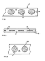
- The present invention is further understood by the Drawings, which form a portion of the present specification, wherein:
- Figure 1 is a perspective view showing the dicing film and its adherent conductive adhesive patterns for contact with the printed wafer;
- Figure 2 is an enlarged cross-sectional view of a section of an embodiment of the dicing film suitable for use with the process of the present invention;
- Figure 3 is an overhead view of a dicing film embodiment suitable for use with the process of the present invention;
- Figure 4 shows an embodiment in which a wafer is about to be picked up for transfer to the dicing film;
- Figure 5 illustrates alignment of the wafer and adhesive pattern preparatory to attachment of wafer and adhesive; and
- Figure 6 shows the wafer/adhesive attachment procedure.
- The dicing film 11 of the present invention comprises a
polymer support film 12 with onesurface 13 which is substantially free of a release coating, and, attached to thesurface 13, a suitable pattern ofconductive adhesive 14 to receivesemiconductor wafers 15 for later dicing (not shown). Thecarrier film 12 needs to have sufficient support for the selected adhesive pattern while allowing such operations as oven drying. It needs to provide support, for example, for the cut chip after the dicing operation. Thesurface 13 must allow for pick-up of the conductive adhesive/chip combination after the dicing operation without causing injury to the adhesive. Theconductive adhesive 14 must have a sufficient level of conductivity, should have good smoothness to allow for full surface contact between it and the wafer and needs to be either dried or partially cured to a suitably tacky state and held in such a state for use at the wafer attachment stage. It needs to have a sufficient degree of co- hesiveness to allow for its stripping from the support film without destruction of its physical integrity and also to allow stripping of an optional cover film therefrom. The conductive adhesive should have a suitable degree of thickness, e.g., from about 6 to about 40 microns to impart proper adhesion and electrical requirements for grounding the chip to the ground plane. The present invention enables one to place the chip/adhesive combination in a chip carrier such that the adhesive supports the chip but does not cover any substantial area outside its support area. This allows for a more compact configuration for the necessary wires bonding the chip to the carrier, without increasing the possibility of short circuits arising due to close proximity of wire and conductive adhesive. - The polymer forming
support film 12 must also, upon heating as will be described later, have an enhanced release characteristic between it and the conductive adhesive so as to allow for clean separation of adhesive and polymer film without any appreciable residual adhesive remaining on the film. Polyolefin films, such as polypropylene, are one preferred choice. The thickness of the support film can range from about 25 to about 150 microns, with a thickness of 75 - 150 microns being preferred. Films having the preferred, greater thicknesses of 75 -150 microns allow for a somewhat greater degree of safety in view of possible variation in the actual manufacturing tolerances in the dicing operation. An excessively thin film, if cut entirely through due to inherent variations in the manufacturing process, would not provide the needed support for the wafer. - Attached to the exposed
surface 13 of the support film is a suitable pattern ofconductive adhesive 14 to form a point of attachment for thesemiconductor wafers 15 that are to be diced. Generally, the conductive adhesive pattern can comprise a series of circular adhesive marks of a suitable size (e.g., about 2.54 - 15.2 cm.) to approximate the diameter of the wafer to be mounted thereon. The thickness of the adhesive can range from about 5 microns to about 40 microns. Suitable conductive adhesive compositions which can be utilized include those adhesive materials which are loaded with fillers to meet.conductivity requirements (e.g., 2% to about 75%, by weight of a suitable conductive material). Representative conductive materials include finely divided conductive metals (e.g., aluminum, copper, silver, gold, palladium), or carbon black. Representative adhesive materials which can form a matrix for the conductive materials include polyimide, acrylic, epoxy, silicones, and various modified polymeric materials to meet desired thermal and conductivity requirements. - In a preferred embodiment, the dicing film product 11 of the present invention also includes a
suitable release liner 16 over the exposed surface of the adhesive to protect it from contamination and/or damage (e.g., inadvertent destruction of the preferred, substantially flat upper surface). For example, release coated paper can be employed as the release liner material. The release liner can have a lesser release characteristic than thesurface 13. - Figures 4-6 illustrate in a schematic manner in which the dicing film of the present invention can be used. Figure 4 shows a pivotal vacuum plate assembly about to pick up a semiconductor wafer from an
array 19 ofstacked wafers 15. Figure 5 illustrates the configuration of an electric eye 20 guided vacuum plate 21 in aligning wafer and adhesive in response to theregistration mark 22 on thefilm 12. Figure 6 illustrates the wafer attachment step and also illustrates the prior stripping of therelease liner 16 from the conductive adhesive 14/dicing film 12 combination. In actual commercial practice,it is preferred to use a suitable commercially available wafer mounter (e.g., Model 366 from Kulicke and Soffa Industries, Inc.). - The dicing film of the present invention can be formed using conventional lamination and printing operations. The pattern of conductive adhesive can be applied to the dried release layer surface by appropriate printing procedures (e.g., rotary or flat bed screen printing) and then the adhesive is transferred to the
support film 12 by lamination. If a release liner is desired over the exposed surface of the adhesive, it can also be applied by conventional lamination procedures. - The heating step of the present process, which improves the release characteristics at the
support film surface 13/conductive adhesive 14 interface, is carried out on the wafer/adhesive/film composite prior to the dicing step. This heating step can take place for about 0.25 min. to about 3 min. at temperatures of from about 45°C. to about 70°C. After dicing, cool air can be used on the carrier film side to optimize die release. By use of the heating step and optional cool air steps, non-release coated, polymeric materials can be more effectively used as support films in dicing films of the general type originally disclosed in my pending U. S. application Serial No. 519,936. - The heating step which is described for use herein aids in wetting out of the adhesive and improves the adhesion between the wafer and the adhesive so that the adhesive will bond substantially more aggressively to the wafer than to the support film. This will insure clean removal of the adhesive with the wafer, as desired.
- The present invention is further illustrated by the Examples which follow.
- This Example illustrates the inferior results obtained when the process of the present invention is not followed.
- The general procedure used to form each of the samples that were tested involved screen printing of a suitable adhesive pattern (i.e., a succession of circles having a diameter of about 7.6 cm. and a thickness of about 25.4 microns)onto release coated paper. The release coated paper was 42 pound weight semi-bleached kraft paper. The adhesive was a silver modified polyimide (P-1011 brand from Epoxy Technology, Inc.). The resulting laminate was then oven dried for 25 minutes at about 67.2°C. and then cooled to room temperature.
- The laminate made by the foregoing procedure was passed through a pressure nip with the selected support film such that the adhesive pattern faced the support film to laminate the adhesive pattern thereto. Sufficient pressure was used to effect such transfer and the composite was heated to about 67.2°C. for one minute.
- The support film selected for use in this Example was 127 micron thick polypropylene (N-400 brand from Hercules) that contained no release coating on the side to which the adhesive pattern was laminated.
- After the adhesive pattern had been transferred to the support films, the same type of paper originally used in the screen printing of the adhesive was used as a cover sheet for the exposed surface of the adhesive pattern. This cover sheet was fed with the adhesive/ support film laminate through two pressure nips so that the release coating and exposed surface of the adhesive pattern were brought together under sufficient pressure to bond the release paper and laminate.
- The type of laminate described above was then tested (after removal of the cover sheet) to determine if the adhesive separated readily from the support film. The following procedure was used. A silicon wafer was affixed to the adhesive by action of a squeegee to eliminate air entrapment. After attachment had been completed, an attempt was made by hand to remove the wafer and its attached adhesive cleanly from the support film.
- One half dozen samples were prepared using the above procedure. When attempts were made to remove the wafer from the support film from each of the samples, it was found that only from about 50% to about 90% of the adhesive transferred cleanly from the support film to the wafer.
- This Example illustrates the process of the present invention.
- The procedure described in Comparative Example 1 was utilized with the exception that the bonded combination of wafer and adhesive/support film laminate was heated for one minute at about 67.2°C. prior to attempting to remove the wafer from the adhesive pattern. When the attempt to remove the wafer was made, substantially all of the adhesive cleanly released from the support film with the wafer.
- The foregoing Examples serve to illustrate certain embodiments of the present invention and should not be construed in a limiting sense. The scope of protection which is sought is given in the claims which follow.
Claims (13)
Applications Claiming Priority (2)
| Application Number | Priority Date | Filing Date | Title |
|---|---|---|---|
| US562899 | 1983-12-19 | ||
| US06/562,899 US4664739A (en) | 1983-12-19 | 1983-12-19 | Removal of semiconductor wafers from dicing film |
Publications (2)
| Publication Number | Publication Date |
|---|---|
| EP0146197A2 true EP0146197A2 (en) | 1985-06-26 |
| EP0146197A3 EP0146197A3 (en) | 1986-12-30 |
Family
ID=24248262
Family Applications (1)
| Application Number | Title | Priority Date | Filing Date |
|---|---|---|---|
| EP84201904A Withdrawn EP0146197A3 (en) | 1983-12-19 | 1984-12-18 | Removal of semiconductor wafers from dicing film |
Country Status (5)
| Country | Link |
|---|---|
| US (1) | US4664739A (en) |
| EP (1) | EP0146197A3 (en) |
| JP (1) | JPS60136331A (en) |
| KR (1) | KR850005148A (en) |
| PH (1) | PH21462A (en) |
Cited By (7)
| Publication number | Priority date | Publication date | Assignee | Title |
|---|---|---|---|---|
| EP0412741A2 (en) * | 1989-08-08 | 1991-02-13 | Nec Corporation | Conductive adhesive sheet used in semiconductor device manufacture |
| EP0423648A1 (en) * | 1989-10-20 | 1991-04-24 | Fujitsu Limited | Wafer processing |
| WO1992007455A1 (en) * | 1990-10-15 | 1992-04-30 | Miroslav Tresky | Device for removing faulty components from circuits |
| EP0510706A2 (en) * | 1991-04-26 | 1992-10-28 | Sumitomo Electric Industries, Ltd. | Apparatus for peeling semiconductor substrate |
| WO2003085702A1 (en) * | 2002-04-04 | 2003-10-16 | Georg Rudolf Sillner | Method for processing electrical components, especially semiconductor chips, and device for carrying out the method |
| CN107442943A (en) * | 2016-05-16 | 2017-12-08 | 株式会社迪思科 | Extend piece |
| CN111217140A (en) * | 2020-01-08 | 2020-06-02 | 歌尔股份有限公司 | Induction material taking device and material taking method thereof |
Families Citing this family (29)
| Publication number | Priority date | Publication date | Assignee | Title |
|---|---|---|---|---|
| PH25206A (en) * | 1985-12-12 | 1991-03-27 | Lintec K K | Control apparatus for reducing adhesive force of adhesive agent adhering between semiconductor wafer and substrate |
| US5030308A (en) * | 1986-07-14 | 1991-07-09 | National Starch And Chemical Investment Holding Corporation | Method of bonding a semiconductor chip to a substrate |
| US4793883A (en) * | 1986-07-14 | 1988-12-27 | National Starch And Chemical Corporation | Method of bonding a semiconductor chip to a substrate |
| US4826553A (en) * | 1987-06-18 | 1989-05-02 | The United States Of America As Represented By The Secretary Of The Air Force | Method for replicating an optical element |
| US4921564A (en) * | 1988-05-23 | 1990-05-01 | Semiconductor Equipment Corp. | Method and apparatus for removing circuit chips from wafer handling tape |
| US5154793A (en) * | 1988-09-27 | 1992-10-13 | General Electric Company | Method and apparatus for removing components bonded to a substrate |
| US5123986A (en) * | 1989-08-10 | 1992-06-23 | Casio Computer Co., Ltd. | Conductive connecting method |
| US5106450A (en) * | 1990-12-20 | 1992-04-21 | International Business Machines Corporation | Dry film resist transport and lamination system for semiconductor wafers |
| US5258236A (en) * | 1991-05-03 | 1993-11-02 | Ibm Corporation | Multi-layer thin film structure and parallel processing method for fabricating same |
| JP3467611B2 (en) * | 1995-09-29 | 2003-11-17 | 日本テキサス・インスツルメンツ株式会社 | Method for manufacturing semiconductor device |
| KR100471936B1 (en) * | 1996-06-04 | 2005-09-09 | 미쓰비시 마테리알 가부시키가이샤 | Wafer cleaning and peeling method and apparatus |
| US5757073A (en) * | 1996-12-13 | 1998-05-26 | International Business Machines Corporation | Heatsink and package structure for wirebond chip rework and replacement |
| JP2000349101A (en) * | 1999-06-07 | 2000-12-15 | Lintec Corp | Transfer tape and use method thereof |
| US6723620B1 (en) * | 1999-11-24 | 2004-04-20 | International Rectifier Corporation | Power semiconductor die attach process using conductive adhesive film |
| US6426552B1 (en) | 2000-05-19 | 2002-07-30 | Micron Technology, Inc. | Methods employing hybrid adhesive materials to secure components of semiconductor device assemblies and packages to one another and assemblies and packages including components secured to one another with such hybrid adhesive materials |
| DE10140827B4 (en) * | 2001-08-21 | 2004-07-29 | Infineon Technologies Ag | Device for debonding thin wafers |
| US6652707B2 (en) | 2002-04-29 | 2003-11-25 | Applied Optoelectronics, Inc. | Method and apparatus for demounting workpieces from adhesive film |
| US6806544B2 (en) | 2002-11-05 | 2004-10-19 | New Wave Research | Method and apparatus for cutting devices from conductive substrates secured during cutting by vacuum pressure |
| US6960813B2 (en) * | 2002-06-10 | 2005-11-01 | New Wave Research | Method and apparatus for cutting devices from substrates |
| US6580054B1 (en) * | 2002-06-10 | 2003-06-17 | New Wave Research | Scribing sapphire substrates with a solid state UV laser |
| JP4107417B2 (en) * | 2002-10-15 | 2008-06-25 | 日東電工株式会社 | Tip workpiece fixing method |
| TWI248244B (en) * | 2003-02-19 | 2006-01-21 | J P Sercel Associates Inc | System and method for cutting using a variable astigmatic focal beam spot |
| JP4283596B2 (en) * | 2003-05-29 | 2009-06-24 | 日東電工株式会社 | Tip workpiece fixing method |
| JPWO2005061227A1 (en) * | 2003-12-24 | 2007-12-13 | 帝人株式会社 | Laminate |
| JP4275522B2 (en) * | 2003-12-26 | 2009-06-10 | 日東電工株式会社 | Dicing die bond film |
| JP4443962B2 (en) * | 2004-03-17 | 2010-03-31 | 日東電工株式会社 | Dicing die bond film |
| EP2063460A4 (en) * | 2006-09-12 | 2011-08-03 | Nitto Denko Corp | Dicing/die bonding film |
| US20130256286A1 (en) * | 2009-12-07 | 2013-10-03 | Ipg Microsystems Llc | Laser processing using an astigmatic elongated beam spot and using ultrashort pulses and/or longer wavelengths |
| US20110132885A1 (en) * | 2009-12-07 | 2011-06-09 | J.P. Sercel Associates, Inc. | Laser machining and scribing systems and methods |
Citations (2)
| Publication number | Priority date | Publication date | Assignee | Title |
|---|---|---|---|---|
| FR2081250A1 (en) * | 1970-03-23 | 1971-12-03 | Silec Semi Conducteurs | Abrasive jet cutting of semiconductor slices - using resin mask |
| US3963551A (en) * | 1974-03-05 | 1976-06-15 | Stromberg-Carlson Corporation | Method for bonding semiconductor chips |
Family Cites Families (4)
| Publication number | Priority date | Publication date | Assignee | Title |
|---|---|---|---|---|
| US3600246A (en) * | 1968-05-17 | 1971-08-17 | Rca Corp | Method of making laminated semiconductor devices |
| GB1299177A (en) * | 1969-01-17 | 1972-12-06 | Ciba Geigy Uk Ltd | Reinforced composites |
| JPS5542326U (en) * | 1978-09-12 | 1980-03-18 | ||
| JPS59105327A (en) * | 1982-12-08 | 1984-06-18 | Toshiba Corp | Soldering method of semiconductor element |
-
1983
- 1983-12-19 US US06/562,899 patent/US4664739A/en not_active Expired - Fee Related
-
1984
- 1984-11-06 KR KR1019840006939A patent/KR850005148A/en not_active IP Right Cessation
- 1984-11-27 JP JP59248846A patent/JPS60136331A/en active Granted
- 1984-12-05 PH PH31535A patent/PH21462A/en unknown
- 1984-12-18 EP EP84201904A patent/EP0146197A3/en not_active Withdrawn
Patent Citations (2)
| Publication number | Priority date | Publication date | Assignee | Title |
|---|---|---|---|---|
| FR2081250A1 (en) * | 1970-03-23 | 1971-12-03 | Silec Semi Conducteurs | Abrasive jet cutting of semiconductor slices - using resin mask |
| US3963551A (en) * | 1974-03-05 | 1976-06-15 | Stromberg-Carlson Corporation | Method for bonding semiconductor chips |
Cited By (10)
| Publication number | Priority date | Publication date | Assignee | Title |
|---|---|---|---|---|
| EP0412741A2 (en) * | 1989-08-08 | 1991-02-13 | Nec Corporation | Conductive adhesive sheet used in semiconductor device manufacture |
| EP0412741A3 (en) * | 1989-08-08 | 1991-11-27 | Nec Corporation | Conductive adhesive sheet used in semiconductor device manufacture |
| EP0423648A1 (en) * | 1989-10-20 | 1991-04-24 | Fujitsu Limited | Wafer processing |
| WO1992007455A1 (en) * | 1990-10-15 | 1992-04-30 | Miroslav Tresky | Device for removing faulty components from circuits |
| EP0510706A2 (en) * | 1991-04-26 | 1992-10-28 | Sumitomo Electric Industries, Ltd. | Apparatus for peeling semiconductor substrate |
| EP0510706A3 (en) * | 1991-04-26 | 1993-01-20 | Sumitomo Electric Industries, Ltd. | Apparatus for peeling semiconductor substrate |
| US5240546A (en) * | 1991-04-26 | 1993-08-31 | Sumitomo Electric Industries, Ltd. | Apparatus for peeling semiconductor substrate |
| WO2003085702A1 (en) * | 2002-04-04 | 2003-10-16 | Georg Rudolf Sillner | Method for processing electrical components, especially semiconductor chips, and device for carrying out the method |
| CN107442943A (en) * | 2016-05-16 | 2017-12-08 | 株式会社迪思科 | Extend piece |
| CN111217140A (en) * | 2020-01-08 | 2020-06-02 | 歌尔股份有限公司 | Induction material taking device and material taking method thereof |
Also Published As
| Publication number | Publication date |
|---|---|
| PH21462A (en) | 1987-10-28 |
| JPS60136331A (en) | 1985-07-19 |
| JPH0334853B2 (en) | 1991-05-24 |
| US4664739A (en) | 1987-05-12 |
| EP0146197A3 (en) | 1986-12-30 |
| KR850005148A (en) | 1985-08-21 |
Similar Documents
| Publication | Publication Date | Title |
|---|---|---|
| US4664739A (en) | Removal of semiconductor wafers from dicing film | |
| US4961804A (en) | Carrier film with conductive adhesive for dicing of semiconductor wafers and dicing method employing same | |
| EP0134606B1 (en) | Carrier film with conductive adhesive for dicing of semiconductor wafers | |
| US5158818A (en) | Conductive die attach tape | |
| US5049434A (en) | Pre-patterned device substrate device-attach adhesive transfer system | |
| US4959008A (en) | Pre-patterned circuit board device-attach adhesive transfer system | |
| US5882956A (en) | Process for producing semiconductor device | |
| US6007920A (en) | Wafer dicing/bonding sheet and process for producing semiconductor device | |
| KR970009574B1 (en) | Adhesive tapes for die bonding | |
| JP3521099B2 (en) | Adhesive sheet for preventing adhesion of adhesive to dicing ring frame and wafer processing sheet provided with the adhesive sheet | |
| EP0253444B1 (en) | Method of bonding a semiconductor chip to a substrate | |
| KR100655035B1 (en) | Process for producing semiconductor device | |
| JP2005507172A (en) | Adhesive wafer for die attach applications | |
| JP4180206B2 (en) | Manufacturing method of semiconductor device | |
| KR19980064239A (en) | Chip manufacturing method and adhesive sheet for manufacturing the chip | |
| JP3592018B2 (en) | Polyimide adhesive sheet and process film for polyimide | |
| JP3744927B2 (en) | Method for manufacturing encapsulated electronic components, in particular integrated circuits | |
| JP5597422B2 (en) | Method for manufacturing electronic component with adhesive film and method for manufacturing mounting body | |
| EP0150882B1 (en) | Conductive die attach tape | |
| US7262114B2 (en) | Die attaching method of semiconductor chip using warpage prevention material | |
| US20070166500A1 (en) | Dicing/die bonding film and method of manufacturing the same | |
| JP4343493B2 (en) | Method for stacking semiconductor chips | |
| CN103305138A (en) | Pressure-sensitive adhesive tape for resin sealing and production method for resin sealing type semiconductor device | |
| JPH10233373A (en) | Manufacture of chip body and adhesive sheet used in the manufacture | |
| JP4045674B2 (en) | IC chip connection method |
Legal Events
| Date | Code | Title | Description |
|---|---|---|---|
| PUAI | Public reference made under article 153(3) epc to a published international application that has entered the european phase |
Free format text: ORIGINAL CODE: 0009012 |
|
| AK | Designated contracting states |
Designated state(s): DE FR GB IT NL |
|
| PUAL | Search report despatched |
Free format text: ORIGINAL CODE: 0009013 |
|
| AK | Designated contracting states |
Kind code of ref document: A3 Designated state(s): DE FR GB IT NL |
|
| 17P | Request for examination filed |
Effective date: 19870629 |
|
| RAP1 | Party data changed (applicant data changed or rights of an application transferred) |
Owner name: NATIONAL STARCH AND CHEMICAL CORPORATION |
|
| 17Q | First examination report despatched |
Effective date: 19900730 |
|
| STAA | Information on the status of an ep patent application or granted ep patent |
Free format text: STATUS: THE APPLICATION IS DEEMED TO BE WITHDRAWN |
|
| 18D | Application deemed to be withdrawn |
Effective date: 19910703 |
|
| RIN1 | Information on inventor provided before grant (corrected) |
Inventor name: AURICHIO, JOSEPH ANTHONY |