EP0144683B1 - Alignment layer orientation in liquid crystal displays - Google Patents
Alignment layer orientation in liquid crystal displays Download PDFInfo
- Publication number
- EP0144683B1 EP0144683B1 EP84112874A EP84112874A EP0144683B1 EP 0144683 B1 EP0144683 B1 EP 0144683B1 EP 84112874 A EP84112874 A EP 84112874A EP 84112874 A EP84112874 A EP 84112874A EP 0144683 B1 EP0144683 B1 EP 0144683B1
- Authority
- EP
- European Patent Office
- Prior art keywords
- layer
- substrate
- liquid crystal
- alignment
- antireflectance
- Prior art date
- Legal status (The legal status is an assumption and is not a legal conclusion. Google has not performed a legal analysis and makes no representation as to the accuracy of the status listed.)
- Expired
Links
- 239000004973 liquid crystal related substance Substances 0.000 title claims description 33
- 239000000758 substrate Substances 0.000 claims description 26
- VYPSYNLAJGMNEJ-UHFFFAOYSA-N silicon dioxide Inorganic materials O=[Si]=O VYPSYNLAJGMNEJ-UHFFFAOYSA-N 0.000 claims description 8
- 239000000463 material Substances 0.000 claims description 7
- GLGZJMAYDWXROS-UHFFFAOYSA-N 4-(4-decylphenyl)benzonitrile Chemical group C1=CC(CCCCCCCCCC)=CC=C1C1=CC=C(C#N)C=C1 GLGZJMAYDWXROS-UHFFFAOYSA-N 0.000 claims description 5
- GPGGNNIMKOVSAG-UHFFFAOYSA-N 4-(4-octoxyphenyl)benzonitrile Chemical group C1=CC(OCCCCCCCC)=CC=C1C1=CC=C(C#N)C=C1 GPGGNNIMKOVSAG-UHFFFAOYSA-N 0.000 claims description 4
- YIJBPYUXIFSTAP-UHFFFAOYSA-N 4-(4-undecylphenyl)benzonitrile Chemical group C1=CC(CCCCCCCCCCC)=CC=C1C1=CC=C(C#N)C=C1 YIJBPYUXIFSTAP-UHFFFAOYSA-N 0.000 claims description 4
- 239000004020 conductor Substances 0.000 claims description 3
- 239000000203 mixture Substances 0.000 description 12
- 210000004027 cell Anatomy 0.000 description 5
- 239000011248 coating agent Substances 0.000 description 5
- 238000000576 coating method Methods 0.000 description 5
- 210000002858 crystal cell Anatomy 0.000 description 5
- 239000004990 Smectic liquid crystal Substances 0.000 description 2
- 239000004411 aluminium Substances 0.000 description 2
- 229910052782 aluminium Inorganic materials 0.000 description 2
- XAGFODPZIPBFFR-UHFFFAOYSA-N aluminium Chemical compound [Al] XAGFODPZIPBFFR-UHFFFAOYSA-N 0.000 description 2
- 230000002457 bidirectional effect Effects 0.000 description 2
- 239000005388 borosilicate glass Substances 0.000 description 2
- 238000001704 evaporation Methods 0.000 description 2
- 230000008020 evaporation Effects 0.000 description 2
- 229910052751 metal Inorganic materials 0.000 description 2
- 239000002184 metal Substances 0.000 description 2
- 230000003595 spectral effect Effects 0.000 description 2
- CSQPODPWWMOTIY-UHFFFAOYSA-N 4-(4-octylphenyl)benzonitrile Chemical group C1=CC(CCCCCCCC)=CC=C1C1=CC=C(C#N)C=C1 CSQPODPWWMOTIY-UHFFFAOYSA-N 0.000 description 1
- VYZAMTAEIAYCRO-UHFFFAOYSA-N Chromium Chemical compound [Cr] VYZAMTAEIAYCRO-UHFFFAOYSA-N 0.000 description 1
- 230000015572 biosynthetic process Effects 0.000 description 1
- 229910052804 chromium Inorganic materials 0.000 description 1
- 239000011651 chromium Substances 0.000 description 1
- 210000001787 dendrite Anatomy 0.000 description 1
- 230000001419 dependent effect Effects 0.000 description 1
- 230000008021 deposition Effects 0.000 description 1
- 239000011521 glass Substances 0.000 description 1
- AMGQUBHHOARCQH-UHFFFAOYSA-N indium;oxotin Chemical compound [In].[Sn]=O AMGQUBHHOARCQH-UHFFFAOYSA-N 0.000 description 1
- 229910010272 inorganic material Inorganic materials 0.000 description 1
- 239000011147 inorganic material Substances 0.000 description 1
- 238000004519 manufacturing process Methods 0.000 description 1
- 238000000034 method Methods 0.000 description 1
- 238000012827 research and development Methods 0.000 description 1
- 235000012239 silicon dioxide Nutrition 0.000 description 1
- 239000000377 silicon dioxide Substances 0.000 description 1
- 238000007738 vacuum evaporation Methods 0.000 description 1
- 238000001429 visible spectrum Methods 0.000 description 1
Images

Classifications
-
- G—PHYSICS
- G02—OPTICS
- G02F—OPTICAL DEVICES OR ARRANGEMENTS FOR THE CONTROL OF LIGHT BY MODIFICATION OF THE OPTICAL PROPERTIES OF THE MEDIA OF THE ELEMENTS INVOLVED THEREIN; NON-LINEAR OPTICS; FREQUENCY-CHANGING OF LIGHT; OPTICAL LOGIC ELEMENTS; OPTICAL ANALOGUE/DIGITAL CONVERTERS
- G02F1/00—Devices or arrangements for the control of the intensity, colour, phase, polarisation or direction of light arriving from an independent light source, e.g. switching, gating or modulating; Non-linear optics
- G02F1/01—Devices or arrangements for the control of the intensity, colour, phase, polarisation or direction of light arriving from an independent light source, e.g. switching, gating or modulating; Non-linear optics for the control of the intensity, phase, polarisation or colour
- G02F1/13—Devices or arrangements for the control of the intensity, colour, phase, polarisation or direction of light arriving from an independent light source, e.g. switching, gating or modulating; Non-linear optics for the control of the intensity, phase, polarisation or colour based on liquid crystals, e.g. single liquid crystal display cells
- G02F1/132—Thermal activation of liquid crystals exhibiting a thermo-optic effect
-
- G—PHYSICS
- G02—OPTICS
- G02F—OPTICAL DEVICES OR ARRANGEMENTS FOR THE CONTROL OF LIGHT BY MODIFICATION OF THE OPTICAL PROPERTIES OF THE MEDIA OF THE ELEMENTS INVOLVED THEREIN; NON-LINEAR OPTICS; FREQUENCY-CHANGING OF LIGHT; OPTICAL LOGIC ELEMENTS; OPTICAL ANALOGUE/DIGITAL CONVERTERS
- G02F1/00—Devices or arrangements for the control of the intensity, colour, phase, polarisation or direction of light arriving from an independent light source, e.g. switching, gating or modulating; Non-linear optics
- G02F1/01—Devices or arrangements for the control of the intensity, colour, phase, polarisation or direction of light arriving from an independent light source, e.g. switching, gating or modulating; Non-linear optics for the control of the intensity, phase, polarisation or colour
- G02F1/13—Devices or arrangements for the control of the intensity, colour, phase, polarisation or direction of light arriving from an independent light source, e.g. switching, gating or modulating; Non-linear optics for the control of the intensity, phase, polarisation or colour based on liquid crystals, e.g. single liquid crystal display cells
- G02F1/133—Constructional arrangements; Operation of liquid crystal cells; Circuit arrangements
- G02F1/1333—Constructional arrangements; Manufacturing methods
- G02F1/1335—Structural association of cells with optical devices, e.g. polarisers or reflectors
- G02F1/133502—Antiglare, refractive index matching layers
-
- G—PHYSICS
- G02—OPTICS
- G02F—OPTICAL DEVICES OR ARRANGEMENTS FOR THE CONTROL OF LIGHT BY MODIFICATION OF THE OPTICAL PROPERTIES OF THE MEDIA OF THE ELEMENTS INVOLVED THEREIN; NON-LINEAR OPTICS; FREQUENCY-CHANGING OF LIGHT; OPTICAL LOGIC ELEMENTS; OPTICAL ANALOGUE/DIGITAL CONVERTERS
- G02F1/00—Devices or arrangements for the control of the intensity, colour, phase, polarisation or direction of light arriving from an independent light source, e.g. switching, gating or modulating; Non-linear optics
- G02F1/01—Devices or arrangements for the control of the intensity, colour, phase, polarisation or direction of light arriving from an independent light source, e.g. switching, gating or modulating; Non-linear optics for the control of the intensity, phase, polarisation or colour
- G02F1/13—Devices or arrangements for the control of the intensity, colour, phase, polarisation or direction of light arriving from an independent light source, e.g. switching, gating or modulating; Non-linear optics for the control of the intensity, phase, polarisation or colour based on liquid crystals, e.g. single liquid crystal display cells
- G02F1/133—Constructional arrangements; Operation of liquid crystal cells; Circuit arrangements
- G02F1/1333—Constructional arrangements; Manufacturing methods
- G02F1/1337—Surface-induced orientation of the liquid crystal molecules, e.g. by alignment layers
Definitions
- This invention relates to alignment layer orientation in liquid crystal displays and is more particularly concerned with reflective raster scanned laser addressed liquid crystal displays.
- the alignment of liquid crystal molecules in liquid crystal devices is important for obtaining a high contrast ratio.
- the purpose of the alignment layers is to give a preferred direction to the liquid crystal molecules in the neighbourhood of the surface. That is, it determines the angle the liquid crystal director makes with the plane of the alignment layer.
- the patent to Sprokel, U.S. 4,261,650 describes a method for producing uniform parallel alignment in liquid crystal cells and discusses random in-plane alignment as shown in Figure 1A, alignment with the molecules being tilted out of the plane of the substrate surface as shown in Figure 1B and parallel alignment in the plane of the substrate surface as shown in Figure 1C. This patent did not discuss the angle between the raster scan direction and the liquid crystal director as projected onto the plane of the alignment layer.
- Liquid crystal mixtures have been used for display devices. Liquid crystal mixtures are described in the IBM Technical Disclosure Bulletin Vol. 19, No. 4, September 1976, page 1401 in which a mixture of 4 - octyl - 4' - cyanobiphenyl, and 4 - n - decyl - 4' - cyanobiphenyl is disclosed. Another mixture is described containing 4 - n - octyloxy - 4' - cyanobiphenyl, 4 - n - decyl - 4' - cyanobiphenyl, and 4 - n - undecyl - 4' - cyanobiphenyl. No percentages of this composition were disclosed.
- the invention provides a reflective raster scanned laser addressed liquid crystal display device having first and second substrates separated by a spacing member to form a cavity, said device comprising an alignment layer on said first substrate, and being characterised in that said alignment layer is oriented in a direction perpendicular, parallel or antiparallel to the direction of the scanning raster whereby the orientation direction of the alignment layer determines the characteristics of the written image and wherein the cell includes a liquid crystal material in the cavity, said material comprising
- the orientation of the alignment layer in the thermally addressed smectic liquid crystal display device is chosen relative to the writing orientation to accentuate a selected characteristic.
- the orientation of the alignment layer in a thermally addressed smectic liquid crystal device is chosen relative to the writing direction to accentuate a selected characteristic.
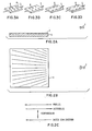
- the alignment layer may be formed by vacuum evaporation of an inert inorganic material at a shallow oblique angle such as described in the patent to Janning, U.S. 3,834,792. This technique usually results in the formation of a textured dendritic structure with the axes of the dendrites formed in the general direction of the evaporation source 1 as shown in Figure 2A.
- the microscopic structure of the alignment layer 2 is related to the source 1-to-substrate 3 orientation during deposition. This directionality is shown schematically in Figure 2B for the special case of a point source aligned with the centreline of the substrate. In practice the lines are in fact more parallel than shown in Figure 2B. If a rectilinear coordinate system coincident with the sides 4 of a rectangular (or square) substrate is imposed on the cell, there are three significantly different directions, shown in Figure 2C as perpendicular, parallel and antiparallel.
- the direction of the raster scan 5 forms an angle ⁇ with the direction of the projection of the liquid crystal director 6 onto the plane of the alignment layer.
- the angle 8 may vary from 0 to 180°C.
- the angle 8 is restricted to be an angle of 90° as shown in Figure 3B, an angle of 0° as shown in Figure 3C and/or an angle of 180° as shown in Figure 3D.
- a liquid crystal display cell suitable for use of this invention is shown in Figure 4.
- a write laser beam 7 strikes an antireflectance coating 8, designed to match the spectral output of the laser, which consists of a top layer of Si0 2 and a bottom layer of Ti0 2 directly on the substrate surface 10B of substrate 10.
- Substrate 10 is typically a borosilicate glass.
- On substrate surface 10A is a three-layer antireflectance coating 13 designed to match the spectral output of the laser which consists of two layers of Ti0 2 on either side of the middle layer of Si0 2 .
- Layer 18 is a conductive metallic absorbing layer which is typically a metal such as chromium.
- a layer 20 is a reflective conductive electrode, for example, of aluminium.
- Layer 19 is an insulating layer of Si0 2 .
- the alignment layer 22 is evaporated at an angle to the substrate to provide the alignment described in either Figure 3B, 3C or 3D.
- Layer 27 is an insulating layer put down at 90°.
- Layer 24 is a transparent conductor electrode layer of a material such as indium tin oxide.
- Substrate 12 is a borosilicate glass and layer 21 is a broad band antireflectance coating for the visible spectrum that consists of a number of layers, for example, 7 to 9 layers, consisting of materials such as TiO 1 , Si0 2 , MgF and the like.
- FIG. 4 shows an LC cell comprising glass substrates 10, 12 having an outer anti-reflection coating 8, 21.
- the substrate 10 carries a second anti-reflection coating 10A, a conductive, metal, light absorbing layer 18, the reflective aluminium layer 20, an insulating silicon dioxide layer 19 and the alignment layer 22.
- the substrate 12 carries the second alignment layer 27 and a transparent conductor layer 24.
- the laser beam 7 sweeps in a direction perpendicular to the plane of the paper and increments vertically.
- the alignment layers 22, 27 are put down so that the liquid crystal directors are orientated parallel to the plane of the layers 22, 27 and perpendicular to the sweep direction of the laser beam.
- the liquid crystal composition in the cavity 14 consists of a mixture of 37.5 ⁇ 0.5 weight% 4 - octyloxy - 4' - cyanobiphenyl, 36.8 ⁇ 0.5 weight percent 4 - decyl - 4' - cyanobiphenyl and 25.7 ⁇ 0.5 weight percent 4 - undecyl - 4' - cyanobiphenyl.
- the following table shows the criticality of the liquid crystal mixture composition.
- the three components of the composition cannot vary by more than ⁇ 0.5 weight percent. Concentrations that vary by more than that amount tend to give poor cell performance as far as the contrast and the presence of a ghost image are concerned.
Landscapes
- Physics & Mathematics (AREA)
- Nonlinear Science (AREA)
- Chemical & Material Sciences (AREA)
- Crystallography & Structural Chemistry (AREA)
- General Physics & Mathematics (AREA)
- Optics & Photonics (AREA)
- Mathematical Physics (AREA)
- Spectroscopy & Molecular Physics (AREA)
- Liquid Crystal (AREA)
- Liquid Crystal Substances (AREA)
Description
- This invention relates to alignment layer orientation in liquid crystal displays and is more particularly concerned with reflective raster scanned laser addressed liquid crystal displays.
- The alignment of liquid crystal molecules in liquid crystal devices is important for obtaining a high contrast ratio. The purpose of the alignment layers is to give a preferred direction to the liquid crystal molecules in the neighbourhood of the surface. That is, it determines the angle the liquid crystal director makes with the plane of the alignment layer. The patent to Sprokel, U.S. 4,261,650, describes a method for producing uniform parallel alignment in liquid crystal cells and discusses random in-plane alignment as shown in Figure 1A, alignment with the molecules being tilted out of the plane of the substrate surface as shown in Figure 1B and parallel alignment in the plane of the substrate surface as shown in Figure 1C. This patent did not discuss the angle between the raster scan direction and the liquid crystal director as projected onto the plane of the alignment layer.
- Dewey et al in the IBM Journal of Research and Development, Vol. 26 No. 2, March 1982, pages 177-185 describes reflective raster-scanned laser addressed liquid crystal cells. In this paper the purpose of the alignment layer was to give a preferred direction of the liquid crystal molecules in the neighbourhood of the surface in a manner similar to that described in the patent above. This article points out that the performance of the liquid crystal cell is highly dependent upon these aligning forces and that a strong uniform alignment such as shown in Figures 1 B and 1 C tend to realign the written scattered texture thereby giving excellent bulk erase properties. This article does not address the angle between the raster scan direction and the liquid crystal director as projected onto the plane of the alignment layer.
- Numerous liquid crystal mixtures have been used for display devices. Liquid crystal mixtures are described in the IBM Technical Disclosure Bulletin Vol. 19, No. 4, September 1976, page 1401 in which a mixture of 4 - octyl - 4' - cyanobiphenyl, and 4 - n - decyl - 4' - cyanobiphenyl is disclosed. Another mixture is described containing 4 - n - octyloxy - 4' - cyanobiphenyl, 4 - n - decyl - 4' - cyanobiphenyl, and 4 - n - undecyl - 4' - cyanobiphenyl. No percentages of this composition were disclosed.
- We have found that there is an important relationship between the raster sweep scan direction during writing and the preferred direction assumed by the liquid crystal medium. In particular a perpendicular alignment with respect to the scan direction produces uniformly written images in both scan directions to allow high quality bidirectional writing. Parallel alignment maximizes the contrast in unidirectional writing. Antiparallel alignment increases the selective erase window and improves the resolution in unidirectionally written pages.
- It is the object of this invention to provide an improved raster-scanned thermally addressed liquid crystal display device having improved contrast in the written image, the written images either being produced uniformly in both scan directions, or having maximized contrast in unidirectional writing.
- Accordingly the invention provides a reflective raster scanned laser addressed liquid crystal display device having first and second substrates separated by a spacing member to form a cavity, said device comprising an alignment layer on said first substrate, and being characterised in that said alignment layer is oriented in a direction perpendicular, parallel or antiparallel to the direction of the scanning raster whereby the orientation direction of the alignment layer determines the characteristics of the written image and wherein the cell includes a liquid crystal material in the cavity, said material comprising
- 4-octyloxy-4'-cyanobiphenyl, 37.5%±0.5 weight percent,
- 4-decyl-4'-cyanobiphenyl 36.8±0.5 weight percent and
- 4-undecyl-4'-cyanobiphenyl 25.7±0.5 weight percent.
- The orientation of the alignment layer in the thermally addressed smectic liquid crystal display device is chosen relative to the writing orientation to accentuate a selected characteristic.
- The invention will now be further described with reference to the accompanying drawings, in which:-
- Figures 1A, B and C are prior art liquid crystal cells showing random in-plane, uniform tilted and uniform in-plane alignment;
- Figures 2A-C show the relationship between the evaporation source and the alignment layer;
- Figures 3A-3D show the relationship between the raster-scanned direction and the orientation of the liquid crystal directors;
- Figure 4 is a liquid crystal cell in accordance with this invention.
- The orientation of the alignment layer in a thermally addressed smectic liquid crystal device, is chosen relative to the writing direction to accentuate a selected characteristic.
- The alignment layer may be formed by vacuum evaporation of an inert inorganic material at a shallow oblique angle such as described in the patent to Janning, U.S. 3,834,792. This technique usually results in the formation of a textured dendritic structure with the axes of the dendrites formed in the general direction of the evaporation source 1 as shown in Figure 2A. The microscopic structure of the
alignment layer 2 is related to the source 1-to-substrate 3 orientation during deposition. This directionality is shown schematically in Figure 2B for the special case of a point source aligned with the centreline of the substrate. In practice the lines are in fact more parallel than shown in Figure 2B. If a rectilinear coordinate system coincident with thesides 4 of a rectangular (or square) substrate is imposed on the cell, there are three significantly different directions, shown in Figure 2C as perpendicular, parallel and antiparallel. - As shown in Figure 3A, the direction of the
raster scan 5 forms an angle θ with the direction of the projection of theliquid crystal director 6 onto the plane of the alignment layer. Theangle 8 may vary from 0 to 180°C. In accordance with this invention, theangle 8 is restricted to be an angle of 90° as shown in Figure 3B, an angle of 0° as shown in Figure 3C and/or an angle of 180° as shown in Figure 3D. - When the alignment layer is oriented so that the
liquid crystal directors 6 are positioned perpendicular to the scan direction of theraster 5 as shown in Figure 3B, uniformly written images in both scan directions allows high quality bidirectional writing thereby improving display performance by reducing writing time. - The parallel alignment where 8=0° as shown in Figure 3C, maximized the contrast in unidirectional writing. An antiparallel alignment that is, where r is 180° as shown in Figure 3C increases the selective erase window and improves the resolution in unidirectional written images. Parallel and antiparallel alignments can be combined in a single image if the display can write bidirectionally. One application of this capability would be to mix text and images with the text written in the high contrast mode and the pictures written in the high resolution mode.
- A liquid crystal display cell suitable for use of this invention is shown in Figure 4. A write laser beam 7 strikes an
antireflectance coating 8, designed to match the spectral output of the laser, which consists of a top layer of Si02 and a bottom layer of Ti02 directly on the substrate surface 10B ofsubstrate 10.Substrate 10 is typically a borosilicate glass. Onsubstrate surface 10A is a three-layer antireflectance coating 13 designed to match the spectral output of the laser which consists of two layers of Ti02 on either side of the middle layer of Si02.Layer 18 is a conductive metallic absorbing layer which is typically a metal such as chromium. Alayer 20 is a reflective conductive electrode, for example, of aluminium.Layer 19 is an insulating layer of Si02. - The
alignment layer 22 is evaporated at an angle to the substrate to provide the alignment described in either Figure 3B, 3C or 3D. Aspacing layer 28 of material such as Mylarforms acavity 14 which is filled with a liquid crystal mixture as will be hereinafter more fully described.Layer 27 is an insulating layer put down at 90°.Layer 24 is a transparent conductor electrode layer of a material such as indium tin oxide.Substrate 12 is a borosilicate glass andlayer 21 is a broad band antireflectance coating for the visible spectrum that consists of a number of layers, for example, 7 to 9 layers, consisting of materials such as TiO1, Si02, MgF and the like. - To reiterate Figure 4 shows an LC cell comprising
glass substrates anti-reflection coating substrate 10 carries a secondanti-reflection coating 10A, a conductive, metal,light absorbing layer 18, thereflective aluminium layer 20, an insulatingsilicon dioxide layer 19 and thealignment layer 22. Thesubstrate 12 carries thesecond alignment layer 27 and atransparent conductor layer 24. The laser beam 7 sweeps in a direction perpendicular to the plane of the paper and increments vertically. Thealignment layers layers - The liquid crystal composition in the
cavity 14 consists of a mixture of 37.5±0.5 weight% 4 - octyloxy - 4' - cyanobiphenyl, 36.8±0.5 weight percent 4 - decyl - 4' - cyanobiphenyl and 25.7±0.5 weight percent 4 - undecyl - 4' - cyanobiphenyl. The following table shows the criticality of the liquid crystal mixture composition. The three components of the composition cannot vary by more than ±0.5 weight percent. Concentrations that vary by more than that amount tend to give poor cell performance as far as the contrast and the presence of a ghost image are concerned. -

Claims (4)
Applications Claiming Priority (2)
| Application Number | Priority Date | Filing Date | Title |
|---|---|---|---|
| US06/560,475 US4585310A (en) | 1983-12-12 | 1983-12-12 | Alignment layer orientation in raster scan thermally addressed smectic liquid crystal displays |
| US560475 | 1983-12-12 |
Publications (3)
| Publication Number | Publication Date |
|---|---|
| EP0144683A2 EP0144683A2 (en) | 1985-06-19 |
| EP0144683A3 EP0144683A3 (en) | 1986-01-08 |
| EP0144683B1 true EP0144683B1 (en) | 1990-01-03 |
Family
ID=24237972
Family Applications (1)
| Application Number | Title | Priority Date | Filing Date |
|---|---|---|---|
| EP84112874A Expired EP0144683B1 (en) | 1983-12-12 | 1984-10-26 | Alignment layer orientation in liquid crystal displays |
Country Status (5)
| Country | Link |
|---|---|
| US (1) | US4585310A (en) |
| EP (1) | EP0144683B1 (en) |
| JP (1) | JPS6117122A (en) |
| CA (1) | CA1247726A (en) |
| DE (1) | DE3480956D1 (en) |
Families Citing this family (9)
| Publication number | Priority date | Publication date | Assignee | Title |
|---|---|---|---|---|
| JPS60262130A (en) * | 1984-06-09 | 1985-12-25 | Sony Corp | Liquid-crystal display device |
| GB2177227B (en) * | 1985-06-14 | 1989-12-28 | Semiconductor Energy Lab | Optical non-volatile liquid crystal memory |
| US4787713A (en) * | 1987-05-22 | 1988-11-29 | The Mead Corporation | Transparent laser-addressed liquid crystal light modulator cell |
| CA2123658C (en) * | 1993-05-19 | 1999-01-19 | Willis H. Smith, Jr. | Inducing tilted parallel alignment in liquid crystals |
| US6929953B1 (en) * | 1998-03-07 | 2005-08-16 | Robert A. Levine | Apparatus for analyzing biologic fluids |
| US6587097B1 (en) | 2000-11-28 | 2003-07-01 | 3M Innovative Properties Co. | Display system |
| US6798189B2 (en) | 2001-06-14 | 2004-09-28 | Koa Corporation | Current detection resistor, mounting structure thereof and method of measuring effective inductance |
| DE10329439A1 (en) * | 2003-07-01 | 2005-01-27 | Daimlerchrysler Ag | Cabriolet vehicle with a hardtop |
| US20060215095A1 (en) * | 2005-03-26 | 2006-09-28 | Qin Liu | Laser-writing alignment marks on alignment layer to align liquid crystals |
Family Cites Families (13)
| Publication number | Priority date | Publication date | Assignee | Title |
|---|---|---|---|---|
| US3655269A (en) * | 1971-01-25 | 1972-04-11 | Rca Corp | Liquid crystal display assembly having independent contrast and speed of response controls |
| US3834729A (en) * | 1971-09-23 | 1974-09-10 | Nissan Motor | Sealing unit for pressurized gas generator of automotive safety device |
| GB1452826A (en) * | 1973-10-17 | 1976-10-20 | Secr Defence | Liquid crystal compositions |
| JPS49122748A (en) * | 1973-03-24 | 1974-11-25 | ||
| FR2292253A1 (en) * | 1974-11-21 | 1976-06-18 | Thomson Csf | METHOD AND DEVICE USING A THERMO-OPTICAL EFFECT IN A LIQUID CRYSTAL FOR THE REPRODUCTION OF IMAGES IN REAL TIME AND WITHOUT MEMORY |
| US4221471A (en) * | 1977-06-24 | 1980-09-09 | Motorola, Inc. | Liquid crystal memory device and method of utilizing same |
| US4291948A (en) * | 1977-11-10 | 1981-09-29 | International Standard Electric Corporation | Liquid crystal display incorporating positive and negative smectic material |
| US4261650A (en) * | 1978-12-18 | 1981-04-14 | International Business Machines Corporation | Method for producing uniform parallel alignment in liquid crystal cells |
| US4277147A (en) * | 1979-01-15 | 1981-07-07 | General Motors Corporation | Display device having reduced electrochromic film dissolution |
| JPS5624318A (en) * | 1979-08-02 | 1981-03-07 | Seiko Epson Corp | Liquid crystal matrix display panel |
| US4367924A (en) * | 1980-01-08 | 1983-01-11 | Clark Noel A | Chiral smectic C or H liquid crystal electro-optical device |
| US4422732A (en) * | 1981-06-08 | 1983-12-27 | Ditzik Richard J | Beam addressed electrooptic display system |
| FR2507802A1 (en) * | 1981-06-10 | 1982-12-17 | Thomson Csf | LIQUID CRYSTAL DISPLAY DEVICE HAVING TWO ADDRESSING MODES |
-
1983
- 1983-12-12 US US06/560,475 patent/US4585310A/en not_active Expired - Fee Related
-
1984
- 1984-09-26 CA CA000464051A patent/CA1247726A/en not_active Expired
- 1984-10-20 JP JP59219413A patent/JPS6117122A/en active Granted
- 1984-10-26 EP EP84112874A patent/EP0144683B1/en not_active Expired
- 1984-10-26 DE DE8484112874T patent/DE3480956D1/en not_active Expired - Lifetime
Also Published As
| Publication number | Publication date |
|---|---|
| EP0144683A2 (en) | 1985-06-19 |
| JPS6117122A (en) | 1986-01-25 |
| JPS647365B2 (en) | 1989-02-08 |
| US4585310A (en) | 1986-04-29 |
| DE3480956D1 (en) | 1990-02-08 |
| EP0144683A3 (en) | 1986-01-08 |
| CA1247726A (en) | 1988-12-28 |
Similar Documents
| Publication | Publication Date | Title |
|---|---|---|
| CA1130486A (en) | Bistable liquid crystal twist cell | |
| US5446339A (en) | Cathode ray tube having antistatic/anti-reflection film-covered transparent material laminated body | |
| US4585310A (en) | Alignment layer orientation in raster scan thermally addressed smectic liquid crystal displays | |
| JPH0643461A (en) | Liquid crystal display device | |
| JPH0656459B2 (en) | Liquid crystal display element | |
| GB2230105A (en) | Method of manufacturing ferroelectric liquid crystal display element | |
| KR20010072055A (en) | Improving the angle of view of a lcd screen by novel birefringent film stacking | |
| US4882207A (en) | Ferroelectric liquid crystal cells | |
| KR0159969B1 (en) | Liquid crystal element and liquid crystal device for driving the same | |
| EP0371506A2 (en) | Liquid crystal display device | |
| Sotta | Equilibrium shape of lyotropic cubic monocrystals | |
| Pozhidaev et al. | Low voltage and high optical quality polymer dispersed FLC films | |
| JPH0213926A (en) | liquid crystal device | |
| JP2983724B2 (en) | Alignment treatment method for ferroelectric liquid crystal devices | |
| JP3252294B2 (en) | Liquid crystal display device | |
| JP2645754B2 (en) | Liquid crystal element | |
| JPH05232476A (en) | Liquid crystal display element | |
| JPS61236523A (en) | Smectic liquid crystal display panel | |
| KR950011957B1 (en) | Rubbing method of liquid crystal display device | |
| Dewey | Projection Storage Displays Using Laser-Addressed Smectic Liquid Crystals | |
| JP3029179B2 (en) | Liquid crystal element | |
| JP3060146B2 (en) | Liquid crystal element and liquid crystal display | |
| RU2024103C1 (en) | Optical-relay tube target | |
| JPH06194695A (en) | Optical deflector | |
| JPS6230224A (en) | Smectic liquid crystal device |
Legal Events
| Date | Code | Title | Description |
|---|---|---|---|
| PUAI | Public reference made under article 153(3) epc to a published international application that has entered the european phase |
Free format text: ORIGINAL CODE: 0009012 |
|
| 17P | Request for examination filed |
Effective date: 19841214 |
|
| AK | Designated contracting states |
Designated state(s): DE FR GB IT |
|
| PUAL | Search report despatched |
Free format text: ORIGINAL CODE: 0009013 |
|
| AK | Designated contracting states |
Designated state(s): DE FR GB IT |
|
| 17Q | First examination report despatched |
Effective date: 19870714 |
|
| GRAA | (expected) grant |
Free format text: ORIGINAL CODE: 0009210 |
|
| AK | Designated contracting states |
Kind code of ref document: B1 Designated state(s): DE FR GB IT |
|
| REF | Corresponds to: |
Ref document number: 3480956 Country of ref document: DE Date of ref document: 19900208 |
|
| ET | Fr: translation filed | ||
| ITF | It: translation for a ep patent filed | ||
| PLBE | No opposition filed within time limit |
Free format text: ORIGINAL CODE: 0009261 |
|
| STAA | Information on the status of an ep patent application or granted ep patent |
Free format text: STATUS: NO OPPOSITION FILED WITHIN TIME LIMIT |
|
| 26N | No opposition filed | ||
| ITTA | It: last paid annual fee | ||
| PGFP | Annual fee paid to national office [announced via postgrant information from national office to epo] |
Ref country code: GB Payment date: 19950926 Year of fee payment: 12 |
|
| PGFP | Annual fee paid to national office [announced via postgrant information from national office to epo] |
Ref country code: FR Payment date: 19951009 Year of fee payment: 12 |
|
| PGFP | Annual fee paid to national office [announced via postgrant information from national office to epo] |
Ref country code: DE Payment date: 19951030 Year of fee payment: 12 |
|
| PG25 | Lapsed in a contracting state [announced via postgrant information from national office to epo] |
Ref country code: GB Effective date: 19961026 |
|
| GBPC | Gb: european patent ceased through non-payment of renewal fee |
Effective date: 19961026 |
|
| PG25 | Lapsed in a contracting state [announced via postgrant information from national office to epo] |
Ref country code: FR Effective date: 19970630 |
|
| PG25 | Lapsed in a contracting state [announced via postgrant information from national office to epo] |
Ref country code: DE Effective date: 19970701 |
|
| REG | Reference to a national code |
Ref country code: FR Ref legal event code: ST |