EP0142737B1 - Elektrochemische Technik für die Herstellung einer dielektrischen Isolationsstruktur - Google Patents
Elektrochemische Technik für die Herstellung einer dielektrischen Isolationsstruktur Download PDFInfo
- Publication number
- EP0142737B1 EP0142737B1 EP19840112839 EP84112839A EP0142737B1 EP 0142737 B1 EP0142737 B1 EP 0142737B1 EP 19840112839 EP19840112839 EP 19840112839 EP 84112839 A EP84112839 A EP 84112839A EP 0142737 B1 EP0142737 B1 EP 0142737B1
- Authority
- EP
- European Patent Office
- Prior art keywords
- layer
- moats
- etching
- conductivity type
- depth
- Prior art date
- Legal status (The legal status is an assumption and is not a legal conclusion. Google has not performed a legal analysis and makes no representation as to the accuracy of the status listed.)
- Expired - Lifetime
Links
- 238000000034 method Methods 0.000 title claims description 40
- 238000002955 isolation Methods 0.000 title description 12
- 238000005530 etching Methods 0.000 claims description 45
- 239000012535 impurity Substances 0.000 claims description 20
- 239000000463 material Substances 0.000 claims description 17
- 239000002131 composite material Substances 0.000 claims description 12
- 239000004065 semiconductor Substances 0.000 claims description 7
- 230000008021 deposition Effects 0.000 claims description 6
- 238000004519 manufacturing process Methods 0.000 claims description 5
- 239000000758 substrate Substances 0.000 description 15
- 230000008569 process Effects 0.000 description 12
- 238000009792 diffusion process Methods 0.000 description 11
- 238000000227 grinding Methods 0.000 description 7
- 230000000873 masking effect Effects 0.000 description 6
- KRHYYFGTRYWZRS-UHFFFAOYSA-N Fluorane Chemical compound F KRHYYFGTRYWZRS-UHFFFAOYSA-N 0.000 description 4
- BASFCYQUMIYNBI-UHFFFAOYSA-N platinum Chemical compound [Pt] BASFCYQUMIYNBI-UHFFFAOYSA-N 0.000 description 4
- 238000005498 polishing Methods 0.000 description 4
- ZOXJGFHDIHLPTG-UHFFFAOYSA-N Boron Chemical compound [B] ZOXJGFHDIHLPTG-UHFFFAOYSA-N 0.000 description 3
- 230000015572 biosynthetic process Effects 0.000 description 3
- 229910052796 boron Inorganic materials 0.000 description 3
- 230000000694 effects Effects 0.000 description 3
- 239000007858 starting material Substances 0.000 description 3
- 239000002019 doping agent Substances 0.000 description 2
- 239000012530 fluid Substances 0.000 description 2
- 239000007943 implant Substances 0.000 description 2
- 238000003780 insertion Methods 0.000 description 2
- 230000037431 insertion Effects 0.000 description 2
- 230000004048 modification Effects 0.000 description 2
- 238000012986 modification Methods 0.000 description 2
- 230000003647 oxidation Effects 0.000 description 2
- 238000007254 oxidation reaction Methods 0.000 description 2
- 238000012856 packing Methods 0.000 description 2
- 229910052697 platinum Inorganic materials 0.000 description 2
- XLYOFNOQVPJJNP-UHFFFAOYSA-N water Substances O XLYOFNOQVPJJNP-UHFFFAOYSA-N 0.000 description 2
- LFQSCWFLJHTTHZ-UHFFFAOYSA-N Ethanol Chemical compound CCO LFQSCWFLJHTTHZ-UHFFFAOYSA-N 0.000 description 1
- KWYUFKZDYYNOTN-UHFFFAOYSA-M Potassium hydroxide Chemical compound [OH-].[K+] KWYUFKZDYYNOTN-UHFFFAOYSA-M 0.000 description 1
- 229910052581 Si3N4 Inorganic materials 0.000 description 1
- 230000001154 acute effect Effects 0.000 description 1
- 230000002411 adverse Effects 0.000 description 1
- XAGFODPZIPBFFR-UHFFFAOYSA-N aluminium Chemical compound [Al] XAGFODPZIPBFFR-UHFFFAOYSA-N 0.000 description 1
- 229910052782 aluminium Inorganic materials 0.000 description 1
- 229910052787 antimony Inorganic materials 0.000 description 1
- WATWJIUSRGPENY-UHFFFAOYSA-N antimony atom Chemical compound [Sb] WATWJIUSRGPENY-UHFFFAOYSA-N 0.000 description 1
- 230000008859 change Effects 0.000 description 1
- 230000005465 channeling Effects 0.000 description 1
- 238000002050 diffraction method Methods 0.000 description 1
- 238000010438 heat treatment Methods 0.000 description 1
- 230000007246 mechanism Effects 0.000 description 1
- 229910021420 polycrystalline silicon Inorganic materials 0.000 description 1
- 238000012545 processing Methods 0.000 description 1
- HQVNEWCFYHHQES-UHFFFAOYSA-N silicon nitride Chemical compound N12[Si]34N5[Si]62N3[Si]51N64 HQVNEWCFYHHQES-UHFFFAOYSA-N 0.000 description 1
Images

Classifications
-
- H—ELECTRICITY
- H01—ELECTRIC ELEMENTS
- H01L—SEMICONDUCTOR DEVICES NOT COVERED BY CLASS H10
- H01L21/00—Processes or apparatus adapted for the manufacture or treatment of semiconductor or solid state devices or of parts thereof
- H01L21/70—Manufacture or treatment of devices consisting of a plurality of solid state components formed in or on a common substrate or of parts thereof; Manufacture of integrated circuit devices or of parts thereof
- H01L21/71—Manufacture of specific parts of devices defined in group H01L21/70
- H01L21/76—Making of isolation regions between components
- H01L21/762—Dielectric regions, e.g. EPIC dielectric isolation, LOCOS; Trench refilling techniques, SOI technology, use of channel stoppers
- H01L21/76297—Dielectric isolation using EPIC techniques, i.e. epitaxial passivated integrated circuit
Definitions
- the present invention relates to a method of fabricating dielectrically isolated islands according to the introductory part of claim 1.
- Dielectrically isolated integrated circuits generally include a plurality of islands separated from a support on its side and bottom by a dielectric isolation.
- One of the earlier processes for forming these dielectric isolated islands included an anisotropically etching of a first surface of a substrate to form moats, covering the first surface and the moats with a dielectric isolation layer, followed by forming a support layer thereon.
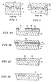
- the structure is illustrated in Figure 1 as having the original substrate 10 with dielectric isolation layer 12 and support layer 14.
- a second surface 16 is mechanically removed down to a line 18 so as to expose the support layer 14 thereby forming dielectrically isolated islands.
- Devices are built in the surface along line 18.
- the second surface 16 is used as a reference plane for the grinding and polishing, any mismatch between surface 16 and the original surface 20 in which the floats are formed will result in the top surface 18 being non-parallel to the bottom surface 20. Since the original substrate 10 must be thick enough to be handled after etching without breaking and subsequently removed by grinding, control of the final thickness and parallelism of surfaces is reduced by grinding tolerances. Thus, the depth of the islands formed must be increased to increase the tolerance to compensate for any mismatching planarity. This unnecessarily increases the surface area of the islands and therefore adversely affects the density on the chip. Since the starting material 10 is also the regions which form the island, different starting resistivity materials must be used depending upon the circuit requirement.
- FIG. 2 Another method of forming dielectric isolation regions is electrochemical etching.
- This method is illustrated in Figure 2 and includes epitaxially forming a second layer 22 on a first layer 24 wherein the first layer 24 has a lower resistivity than the second layer 22.
- the process is continued as in Figure 1 wherein moats are anisotropically formed in the epitaxial layer 22 terminating within the second layer 22 followed by formation of a dielectric isolation layer 26 and a support layer 28.
- the composite structure is then placed in an etching bath and layer 24 is removed by electrochemical etching. This removes the layer 24 down to the interface 30 between the first and second layers 24 and 22.
- Layer 22 is then mechanically removed down to the dash line 32 exposing portions of the support layer 28 to form dielectrically isolated regions.
- Electrochemical etching also has its problems. As noted in U.S. Patent 3,536,600, a tapering effect can be produced and must be corrected. Similarly, because of the subsequent high temperature processing steps, impurities from layer 24 diffuse into layer 22 and consequently the interface layer 30 is not well defined. This induces additional errors in the removal of layer 24 to form a surface 30 which will be mechanically removed. The depth of the final resulting structure between planes 32 and 34 is increased by 10% to account for epitaxial growth errors. By increasing the depth, the lateral surface errors also increase and thereby reduces packing density.
- An object of the present invention to provide a method of forming dielectrically isolated islands wherein a final resulting surface is as parallel as possible to the bottom of the islands and therefore minimizing the depth error or tolerance which will substantially increase density.
- Another object of the present invention is to provide a method of forming dielectrically isolated islands having increased depth accuracy. . -l
- Still another object of the present invention is to provide a method of fabricating dielectrically isolated regions which is capable of tailoring the resulting island resistivity and type while starting with a common substrate.
- the surface in which the moats are etched may be exposed to an introduction of impurities to form buried regions at the surface or to change the conductivity type or impurity concentration of the total resulting dielectrically isolated regions.
- the surface may also be etched and filled by epitaxial deposition of material of opposite conductivity type or increased impurity concentration.
- Figure 1 is a cross-sectional view of a wafer at a stage of fabrication using mechanical removal of the prior art.
- Figure 2 is a cross-sectional view of a wafer using elecromechanical removal of the prior art.
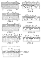
- Figures 3 through 11 are cross-sectional views of a wafer illustrating the method of fabrication incorporating the principles of the present invention.
- Figures 12, 13 and 14 are cross-sectional views illustrating the electrochemical etching step.
- Figures 15, 16 and 17 are cross-sectional views illustrating a wafer during a modified step of the process of Figures 3-11.
- Figure 18 is a cross-sectional view of a wafer which is a further modification of the method of Figures 15-17.
- the process begins with the formation of an epitaxial layer 42 on a substrate 40 having an interface 44 therebetween.
- the original substrate 40 is a relatively high doped material, for example, antimony doped to have a resistance less than 0.05 ohm centimeters and having a [100] oriented parallel faces 44 and 48 parallel to approximately plus or minus two microns.
- the control of the parallelism is not as critical as in prior dielectric isolation processes as will be evident from the following description.
- the epitaxial layer 42 has a resistivity in the range of 0.1 to 100 ohm centimeters depending upon the desired parameters of the resulting structure. The important point being that the difference of resistivity of the substrate 40 and layer 42 should be at least one half an order of magnitude. This is important due to the electrochemical etching step to be described below.
- the epitaxial layer 42 is grown to have a thickness in the range of 7 to 75 microns depending upon the desired island depth. The resulting structure is illustrated in Figure 3.
- a mask layer is formed on exposed surface 46 of the epitaxial layer 42 having openings for the second type island locations.
- Opposite conductivity type impurities for example, P type dopants of, for example, boron or aluminum are then introduced and diffused down to a depth approaching the depth of the epitaxial layer 42.
- the resulting structure is illustrated in Figure 4 wherein a P type impurity region 50 is formed in the epitaxial layer 42.
- a masking step may be performed to introduce N type impurities in the N-epitaxial layer 42 to form a lower resistivity region than the epitaxial layer 42 but not as low as the N+ substrate 40 (not illustrated). This allows an integrated circuit having both analog devices formed in high resistivity region and digital devices are formed in the low resistivity device islands.
- the masking layer is removed and a new masking layer is formed by, for example, oxidation and patterned to form high impurity concentration buried layers.
- N type impurities for example, are introduced and diffused to the required sheet resistivity and penatration. This is illustrated in Figure 5 as N+ region 52.
- the formation of the P region 50 may be eliminated and the surface 46 may be non-selectively subjected to an N+ implant and diffusion. This would result in all the dielectrically isolated islands having a buried N+ layer.
- a buried layer may be formed in P region by introducing P+ impurities through a separate masking step using a boron deposition or implant and diffusion cycle.
- a mask layer 54 is formed on the surface 46 of the epitaxial layer 42 and patterned for openings to form the moats for the isolation walls as well as the scribe lines. Moats are anisotropically etched through the pattern using, for example, a water, alcohol, potasium hydroxide solution. Moats between the dielectrically isolated islands are allowed to V-out and the scribe line moats which encircle the eventually to be formed circuit chips are allowed to etch deeper. As is well known, the depth of the V is a function of the cross-section of the aperture. As illustrated in Figure 6, the island moats terminate within the epitaxial layer 42 while the scribe line moats 58 extend through the epitaxial layer and into the original starting material 40.
- the scribe line moats 58 are shown not to V-out, they may be allowed to V-out if desired. It is preferential that they do not V-out and form a flat surface 60 at the bottom thereof. By the crystallography, the flat surface 60 is parallel to the original surface 46 of the epitaxial layer 42. As will be explained more fully with reference to Figures 12, 13 and 14, the moats 56 terminate a sufficient distance from interface 44 such that the electrochemical etching will not reach the minimum island V-out. As discussed previously, N type impurities from substrate 40 diffuse into epitaxial layer 42 thereby moving the interface of impurities 44 from the original epitaxial interface. Thus, the deeper moats 58 need not extend into the original substrate 40, but only past the lower impurity concentration portion of epitaxial layer 42.
- the masking layer 54 is removed and the surface of the moats 56 and 58 and surface 46 of the epitaxial layer are clean and a dielectric layer 61 is formed thereon.
- this layer may be an oxide layer formed by thermal oxidation or may be a deposited layer.
- this dielectric layer may be silicon nitride, or an oxide-nitride combination.
- a polycrystalline silicon layer is then deposited to a thickness applicable to providing a final, specified, dielectrically isolated slice thickness.
- the polycrystalline layer forms a support 62 illustrated in Figure 7.
- the exposed polycrystalline surface is ground to thicknesses compatible to final dielectric isolation wafer thickness and to remove the top surface grooves caused by the deposition in the moat pattern. While the planarity of this surface and the parallelism to the surface of the original substrate are important, namely to be within the plus or minus two micron range, they are not nearly as critical as in the prior dielectric isolation material processes.
- the slice is inverted and the N+ substrate region 40 is mechanically ground to approximately 35 micron thickness from the epitaxial interface 44. This grinding step is also much less critical than the corresponding grind or lap or etch using prior dielectric isolation material processes.
- the resulting structure is illustrated in Figure 8. As will be discussed below, the thickness of the N+ layer 40 must be sufficient depending upon its resistivity, electric potential, and the etching bath to support electrochemical etching.
- the composite structure of Figure 8 is moved in a dilute bath of hydrofluoric acid, less than approximately 10% by volume, while a current is applied through the N+ layer 40.
- the slice may be moved relative to the bath or the bath may be moved relative to the slice to provide a narrow etching interface.
- Contact electrodes are on the N+ layer and a platinum screen suspended parallel to the slice in the hydrofluoric etchant.
- the level of etchant moves relative to the slice, the N+ layer is etched away until the low-conductive, higher resistive epitaxial layer 42 is exposed or the total current is pinched off by the encircling oxide scribe line moats 58.
- the best control of the final island dimensions is achieved by using the pinch-off mechanism since it reduces the criticality of the epitaxial thickness variations on the final island dimension control.
- the resulting structure is illustrated in Figure 9 and shows the bottom portion 60 of the moat 58 exposed and a surface 64 of the epitaxial layer 42 exposed.
- the tips of the moats 56 are not exposed.
- a thin polish is performed to remove the updiffused region from the heavily doped substrate 40 which has been removed, to remove the etch stain, and to isolate the island regions to a specific thickness depth. The depth is sufficient such that the polycrystalline layer 62 is exposed at a new surface 66 as illustrated in Figure 10.
- the exposed portions of the scribe line moat 60 provided a plane parallel to the bottom of the moat 46.
- the mechanical removal of the portions of the epitaxial layer 42 will be more parallel to the bottom of the moat than the prior art methods.
- the critical control parameter which limits tolerance variation of the final island dimension is the scribe line moat depth. With only this variation plus the minimal tolerance due to the thin polish, the final island thicknesses can then be controlled to within plus or minus one micron.
- the composite structure of Figure 8 is inserted into the electrochemical bath 70 at a small angle as illustrated in Figure 12. Preferably, this angle is 20° or less.
- the insertion motion is vertical.
- the first N+ layer 40 is etched substantially along the surface of the bath 70 and at a very small angle relative to the interface line 44 between the N+ layer 40 and the N- epitaxial layer 42.
- the phantom line in the figures indicates the original interface prior art etching of layer 40.
- the etching continues. As illustrated in Figure 13, at the far right corner, the etching surface 64 extends into the N- layer 42 below the interface 44. Thus, the portion between the scribe lines 60 tends to dish out with the electrochemical etching surface not being planar. At the point. illustrated in Figure 13, the portion of the layer 40 in the fluid 70 has been reduced thereby increasing the resistance thereof to a value which terminates the electrochemical etching. The net result, as illustrated in Figure 14, is that a portion of the layer 40 remains as a shadow. Thus, not only has the portion of the N- epitaxial region 42 been etched out and dished, but portions of the original layer 40 remain due to the pinch-off of the current flow.
- an N+ region 40 having a resistance below 0.02 ohm centimeters and a thickness of 35 microns was placed in a dilute solution of less than 10% of hydrofluoric acid in water.
- the N+ layer 40 and a platinum screen suspended in the etchant were biased to a voltage of 10 volts and the composite structure was inserted at an angle of 15 and lowered into the bath at a rate of 0.5 inches per hour.
- the extra material or portions of the original layer 40 remaining behind are not a serious problem.
- a more serious problem is the dishing out or etching of the N- layer 42. Not only should there be enough of the layer 42 between the interface 44 and the bottom of the moats 56 such that the dish out etching does not go within the area defined by the bottom of the moats 56, but is has been found that the deep moats 58 should be placed no greater than 1000 microns apart. This minimizes the dishing out effect for the angle of repose described above.
- the P region 50 may be formed by other than diffusion.
- a masking layer 72 is provided on the surface 46 of the epitaxial layer 42 and a window is opened therein and used as an etching mask to etch down to the N+ layer 40.
- the resulting opening 74 is then filled with, for example, P type material 78 by epitaxial growth.
- the P type material and the mask layer 72 are removed by well known processes to result in the planar structure illustrated in Figure 17.
- N type material may be epitaxially grown having an impurity concentration greater than the epitaxial layer 42 but less than the N+ layer 40. This allows the electrochemical etching to differentiate between the two layers.
Landscapes
- Engineering & Computer Science (AREA)
- Microelectronics & Electronic Packaging (AREA)
- Condensed Matter Physics & Semiconductors (AREA)
- General Physics & Mathematics (AREA)
- Manufacturing & Machinery (AREA)
- Computer Hardware Design (AREA)
- Physics & Mathematics (AREA)
- Power Engineering (AREA)
- Element Separation (AREA)
- Weting (AREA)
- Metal-Oxide And Bipolar Metal-Oxide Semiconductor Integrated Circuits (AREA)
- Bipolar Integrated Circuits (AREA)
- Drying Of Semiconductors (AREA)
- Pressure Sensors (AREA)
Claims (20)
- Verfahren zum Herstellen dielektrisch isolierter Inseln, das einschließt:
die Bildung einer zweiten Schicht eines Halbleitermaterials auf einer ersten Schicht Halbleitermaterials, wobei die erste Schicht einen niedrigeren spezifischen Widerstand als die zweite Schicht hat;
das Ätzen der zweiten Schicht, um Gräben zu formen, die sich von einer ersten Oberfläche der Schicht herab erstrecken;
die Bildung einer dielektrischen Schicht auf der ersten Oberfläche der zweiten Schicht und der Gräben;
die Bildung einer Trägerschicht auf der dielektrischen Schicht, wodurch sich eine Verbundstruktur ergibt;
gekennzeichnet durch das Einführen der Verbundstruktur in ein Ätzbad, während die erste Schicht und das Bad vorgespannt werden, um die erste Schicht bis zu der dielektrischen Schicht der Gräben im wesentlichen an der Oberfläche des Ätzbades abzuätzen wahrend sich das Niveau des Ätzmittels relativ zu der Verbundstruktur bewegt;
wobei die Verbundstruktur in das Ätzbad mit genügend langsamer Geschwindigkeit eingeführt wird, so daß das Ätzen aufgrund des Abschnürens des Stromflusses durch nacheinander freigelegte dielektrische Schichten aufeinanderfolgender Gräben beendet wird. - Verfahren nach Anspruch 1, wobei das Ätzen durch Vorspannen der ersten Schicht durchgeführt wird, um elektrischen Strom zu leiten und fortschreitend Teile der ersten Schicht wegzuätzen bis der Stromfluß durch jeden Teil der ersten Schicht durch die nacheinander freigelegten dielektrischen Schichten in den Gräben abgeschnürt ist.
- Verfahren nach Anspruch 1, das weiter einschließt:
Ätzen der zweiten Schicht, um erste Gräben zu formen, die sich von der ersten Oberfläche herab bis zu einer ersten Tiefe erstrecken, und uni zweite Gräben zu formen, die sich von der ersten Oberfläche herab bis zu einer zweiten Tiefe erstrecken, die geringer als die erste Tiefe ist; elektrochemisches Ätzen der ersten Schicht, um die dielektrische Schicht auf den ersten Gräben freizulegen; und Abtragen der dielektrischen Schicht und der zweiten Schicht bis zu einer Ebene herab, die die zweiten Gräben freilegt, und Benutzen der freigelegten Abschnitte der zweiten Gräben als Referenzebene. - Verfahren nach Anspruch 1, wobei das Ätzen durch langsames und kontinuierliches Einführen der Verbundstruktur in das Ätzbad durchgeführt wird, wobei die Oberfläche der ersten Schicht zum Ätzbad zeigt, und einen Winkel mit der Oberfläche des Ätzbades bildet, um eingetauchte Teile der ersten Schicht bis zur Abschnürung durch nacheinander freigelegte dielektrische Schichten von Gräben abzuätzen.
- Verfahren nach Anspruch 4, wobei der flache Winkel weniger als 20 Grad in bezug auf die die Oberfläche des Ätzbades beträgt.
- Verfahren nach Anspruch 2 bis 3, wobei die niedrigeren Gräben so geätzt werden, daß sie innerhalb der zweiten Schicht, in genügender Entfernung von der Grenzfläche der ersten und zweiten Schicht enden, so daß sie nicht durch den elektrochemischen Ätzschritt freigelegt werden.
- Verfahren nach Anspruch 2, 3, 4, 5 oder 6, wobei die tieferen Gräben so geformt sind, daß sie eine Tiefe und seitlichen Abstand in der ersten Schicht haben, um elektrochemisches Ätzen der zweiten Schicht von der Grenzfläche aus zu einer Tiefe unterhalb einer Ebene, die durch die Begrenzungen der niedrigeren Gräben gebildet wird, zu verhindern.
- Verfahren nach einem der Ansprüche 1 bis 7, wobei die Gräben durch anisotropes Ätzen geformt werden.
- Verfahren nach Anspruch 8, wobei der tiefere Graben zu einer Tiefe geätzt wird, die geringer ist als eine voll V-förmig ausgeätzte Tiefe, so daß er eine ebene Begrenzung hat.
- Verfahren nach Anspruch 1, das ein Abtragen eines Teils der ersten Schicht einschließt, um ihre Dicke vor dem elektrochemischen Ätzen zu verringern.
- Verfahren nach Anspruch 1, wobei die zweite Schicht durch Epitaxie gebildet wird.
- Verfahren nach Anspruch 1, das ein Einbringen von Störstellen desselben Leitfähigkeitstyps wie die zweite Schicht in die erste Oberfläche der zweiten Schicht einschließt, um Bereiche reduzierten spezifischen Widerstands in der zweiten Schicht zu bilden bevor die Trägerschicht gebildet wird.
- Verfahren nach Anspruch 1, das ein Einbringen von Störstellen eines zweiten, einem ersten Leitfähigkeitstyp der zweiten Schicht entgegengesetzten Leitfähigkeitstyps, in wahlweise Gebiete der ersten Oberfläche der zweiten Schicht einschließt, um Bereiche des zweiten Leitfähigkeitstyps zu bilden, die sich von der ersten Oberfläche der zweiten Schicht zu der Grenzfläche der ersten und zweiten Schichten erstrecht, bevor die Trägerschicht gebildet wird.
- Verfahren nach Anspruch 13, das das Einbringen von Störstellen des ersten Leitfähigkeitstyps in ausgewählte Gebiete der ersten Oberfläche der zweiten Schicht einschließt, um Bereiche reduzierten spezifischen Widerstands in der zweiten Schicht zu bilden, bevor die Trägerschicht gebildet wird.
- Verfahren nach Anspruch 1, das ein Abtragen voll Teilen der Trägerschicht einschließt, um eine ebene Oberfläche zu schaffen.
- Verfahren nach Anspruch 1, das ein Ätzen der erster, Oberfläche der zweiter, Schicht einschließt, um eine Vertiefung zu formen, die sich von der ersten Oberfläche zu der Grenzfläche zwischen den ersten und zweiten Schichten erstreckt, sowie das Auffüllen der Vertiefung mit einem Halbleitermaterial mit anderen Eigenschaften als der zweiten Schicht, bevor die Trägerschicht gebildet wird.
- Verfahren nach Anspruch 16, wobei der Schritt des Auffüllens der Vertiefung das Aufbringen durch Epitaxie eines Halbleitermaterials mit einem zweiten Leitfähigkeitstyp einschließt, der einem ersten Leitfähigkeitstyp der zweiten Schicht entgegengesetzt ist.
- Verfahren nach Anspruch 16, wobei der Schritt des Auffüllens der Vertiefung das Aufbringen durch Epitaxie von Halbleitermaterial einschließt, das denselben Leitfähigkeitstyp wie die zweite Schicht und einen niedrigeren spezifischen Widerstand als die zweite Schicht und einen höheren spezifischen Widerstand als die erste Schicht besitzt.
- Verfahren nach Anspruch 1, wobei die Verbundstruktur langsam genug in das Ätzbad bewegt wird, so daß das elektrochemische Ätzen beendet wird, bevor die ganze erste Schicht weggeätzt ist.
- Verfahren nach Anspruch 2, wobei die tieferen Gräben einen genügend engen seitlichen Abstand haben, um das Ätzen der zweiten Schicht zu verhindern.
Applications Claiming Priority (2)
| Application Number | Priority Date | Filing Date | Title |
|---|---|---|---|
| US54863183A | 1983-11-04 | 1983-11-04 | |
| US548631 | 1983-11-04 |
Publications (3)
| Publication Number | Publication Date |
|---|---|
| EP0142737A2 EP0142737A2 (de) | 1985-05-29 |
| EP0142737A3 EP0142737A3 (en) | 1987-11-25 |
| EP0142737B1 true EP0142737B1 (de) | 1993-10-06 |
Family
ID=24189713
Family Applications (1)
| Application Number | Title | Priority Date | Filing Date |
|---|---|---|---|
| EP19840112839 Expired - Lifetime EP0142737B1 (de) | 1983-11-04 | 1984-10-25 | Elektrochemische Technik für die Herstellung einer dielektrischen Isolationsstruktur |
Country Status (3)
| Country | Link |
|---|---|
| EP (1) | EP0142737B1 (de) |
| JP (1) | JPH0758735B2 (de) |
| DE (1) | DE3486223T2 (de) |
Families Citing this family (1)
| Publication number | Priority date | Publication date | Assignee | Title |
|---|---|---|---|---|
| US4820653A (en) * | 1988-02-12 | 1989-04-11 | American Telephone And Telegraph Company | Technique for fabricating complementary dielectrically isolated wafer |
Family Cites Families (3)
| Publication number | Priority date | Publication date | Assignee | Title |
|---|---|---|---|---|
| GB1114798A (en) * | 1965-08-09 | 1968-05-22 | Westinghouse Electric Corp | Integrated circuit device with dielectric isolation and method of making the same |
| NL6703014A (de) * | 1967-02-25 | 1968-08-26 | ||
| GB1300710A (en) * | 1970-12-10 | 1972-12-20 | Signetics Corp | Complementary transistor structure and method |
-
1984
- 1984-10-25 EP EP19840112839 patent/EP0142737B1/de not_active Expired - Lifetime
- 1984-10-25 DE DE19843486223 patent/DE3486223T2/de not_active Expired - Fee Related
- 1984-11-05 JP JP59233009A patent/JPH0758735B2/ja not_active Expired - Fee Related
Also Published As
| Publication number | Publication date |
|---|---|
| DE3486223D1 (de) | 1993-11-11 |
| EP0142737A3 (en) | 1987-11-25 |
| JPS60175436A (ja) | 1985-09-09 |
| EP0142737A2 (de) | 1985-05-29 |
| DE3486223T2 (de) | 1994-03-31 |
| JPH0758735B2 (ja) | 1995-06-21 |
Similar Documents
| Publication | Publication Date | Title |
|---|---|---|
| EP0098374B1 (de) | Dielektrische Isolationsstruktur für integrierte Schaltungen und Verfahren zur Herstellung dieser Struktur | |
| US4897362A (en) | Double epitaxial method of fabricating semiconductor devices on bonded wafers | |
| US4211582A (en) | Process for making large area isolation trenches utilizing a two-step selective etching technique | |
| US4929566A (en) | Method of making dielectrically isolated integrated circuits using oxygen implantation and expitaxial growth | |
| EP0296754A2 (de) | Verfahren zur Herstellung von Halbleiteranordnungen mit Gräben als Isolationszonen | |
| EP0166207B1 (de) | Vereinfachtes Planarisationsverfahren für mit Polysilicium gefüllte Gräben | |
| US4554059A (en) | Electrochemical dielectric isolation technique | |
| EP0034910A1 (de) | Verfahren zur Herstellung einer Halbleitervorrichtung und so hergestellte Vorrichtung | |
| US4301588A (en) | Consumable amorphous or polysilicon emitter process | |
| US4965217A (en) | Method of making a lateral transistor | |
| US4900689A (en) | Method of fabrication of isolated islands for complementary bipolar devices | |
| JP3862294B2 (ja) | 半導体装置の製造方法 | |
| US4193836A (en) | Method for making semiconductor structure | |
| US5675173A (en) | Semiconductor device having a trench for isolating elements and a trench for applying a potential to a substrate | |
| US4050979A (en) | Process for thinning silicon with special application to producing silicon on insulator | |
| GB2082386A (en) | Zener diodes and their manufacture | |
| EP0113405B1 (de) | Verfahren zur Herstellung eines Halbleiterwiderstandes | |
| US3829889A (en) | Semiconductor structure | |
| US6486038B1 (en) | Method for and device having STI using partial etch trench bottom liner | |
| EP0142737B1 (de) | Elektrochemische Technik für die Herstellung einer dielektrischen Isolationsstruktur | |
| EP0337720B1 (de) | Verfahren zur Herstellung eines Bipolartransistors | |
| EP0488230B1 (de) | Verfahren zur Herstellung eines Halbleitersubstrates mit einer dielektrischen Isolationsstruktur | |
| US3566219A (en) | Pinched resistor semiconductor structure | |
| KR20000062591A (ko) | 개량된 반도체 트렌치 모스 디바이스 | |
| EP0137195B1 (de) | Dielektrisch isolierte Schaltung und Verfahren zur Herstellung |
Legal Events
| Date | Code | Title | Description |
|---|---|---|---|
| PUAI | Public reference made under article 153(3) epc to a published international application that has entered the european phase |
Free format text: ORIGINAL CODE: 0009012 |
|
| AK | Designated contracting states |
Designated state(s): DE FR GB NL SE |
|
| PUAL | Search report despatched |
Free format text: ORIGINAL CODE: 0009013 |
|
| AK | Designated contracting states |
Kind code of ref document: A3 Designated state(s): DE FR GB NL SE |
|
| 17P | Request for examination filed |
Effective date: 19880205 |
|
| 17Q | First examination report despatched |
Effective date: 19891003 |
|
| GRAA | (expected) grant |
Free format text: ORIGINAL CODE: 0009210 |
|
| AK | Designated contracting states |
Kind code of ref document: B1 Designated state(s): DE FR GB NL SE |
|
| PG25 | Lapsed in a contracting state [announced via postgrant information from national office to epo] |
Ref country code: SE Effective date: 19931006 Ref country code: NL Effective date: 19931006 |
|
| REF | Corresponds to: |
Ref document number: 3486223 Country of ref document: DE Date of ref document: 19931111 |
|
| ET | Fr: translation filed | ||
| NLV1 | Nl: lapsed or annulled due to failure to fulfill the requirements of art. 29p and 29m of the patents act | ||
| PLBE | No opposition filed within time limit |
Free format text: ORIGINAL CODE: 0009261 |
|
| STAA | Information on the status of an ep patent application or granted ep patent |
Free format text: STATUS: NO OPPOSITION FILED WITHIN TIME LIMIT |
|
| 26N | No opposition filed | ||
| REG | Reference to a national code |
Ref country code: GB Ref legal event code: IF02 |
|
| PGFP | Annual fee paid to national office [announced via postgrant information from national office to epo] |
Ref country code: FR Payment date: 20021002 Year of fee payment: 19 |
|
| PGFP | Annual fee paid to national office [announced via postgrant information from national office to epo] |
Ref country code: GB Payment date: 20021016 Year of fee payment: 19 |
|
| PGFP | Annual fee paid to national office [announced via postgrant information from national office to epo] |
Ref country code: DE Payment date: 20021031 Year of fee payment: 19 |
|
| PG25 | Lapsed in a contracting state [announced via postgrant information from national office to epo] |
Ref country code: GB Free format text: LAPSE BECAUSE OF NON-PAYMENT OF DUE FEES Effective date: 20031025 |
|
| PG25 | Lapsed in a contracting state [announced via postgrant information from national office to epo] |
Ref country code: DE Free format text: LAPSE BECAUSE OF NON-PAYMENT OF DUE FEES Effective date: 20040501 |
|
| GBPC | Gb: european patent ceased through non-payment of renewal fee |
Effective date: 20031025 |
|
| PG25 | Lapsed in a contracting state [announced via postgrant information from national office to epo] |
Ref country code: FR Free format text: LAPSE BECAUSE OF NON-PAYMENT OF DUE FEES Effective date: 20040630 |
|
| REG | Reference to a national code |
Ref country code: FR Ref legal event code: ST |