EP0139157A1 - Apparatus for growing single crystals of dissociative compounds - Google Patents
Apparatus for growing single crystals of dissociative compounds Download PDFInfo
- Publication number
- EP0139157A1 EP0139157A1 EP84109948A EP84109948A EP0139157A1 EP 0139157 A1 EP0139157 A1 EP 0139157A1 EP 84109948 A EP84109948 A EP 84109948A EP 84109948 A EP84109948 A EP 84109948A EP 0139157 A1 EP0139157 A1 EP 0139157A1
- Authority
- EP
- European Patent Office
- Prior art keywords
- chamber
- sealed
- pressure
- ceramic
- divided
- Prior art date
- Legal status (The legal status is an assumption and is not a legal conclusion. Google has not performed a legal analysis and makes no representation as to the accuracy of the status listed.)
- Granted
Links
Images

Classifications
-
- C—CHEMISTRY; METALLURGY
- C30—CRYSTAL GROWTH
- C30B—SINGLE-CRYSTAL GROWTH; UNIDIRECTIONAL SOLIDIFICATION OF EUTECTIC MATERIAL OR UNIDIRECTIONAL DEMIXING OF EUTECTOID MATERIAL; REFINING BY ZONE-MELTING OF MATERIAL; PRODUCTION OF A HOMOGENEOUS POLYCRYSTALLINE MATERIAL WITH DEFINED STRUCTURE; SINGLE CRYSTALS OR HOMOGENEOUS POLYCRYSTALLINE MATERIAL WITH DEFINED STRUCTURE; AFTER-TREATMENT OF SINGLE CRYSTALS OR A HOMOGENEOUS POLYCRYSTALLINE MATERIAL WITH DEFINED STRUCTURE; APPARATUS THEREFOR
- C30B15/00—Single-crystal growth by pulling from a melt, e.g. Czochralski method
- C30B15/10—Crucibles or containers for supporting the melt
-
- C—CHEMISTRY; METALLURGY
- C30—CRYSTAL GROWTH
- C30B—SINGLE-CRYSTAL GROWTH; UNIDIRECTIONAL SOLIDIFICATION OF EUTECTIC MATERIAL OR UNIDIRECTIONAL DEMIXING OF EUTECTOID MATERIAL; REFINING BY ZONE-MELTING OF MATERIAL; PRODUCTION OF A HOMOGENEOUS POLYCRYSTALLINE MATERIAL WITH DEFINED STRUCTURE; SINGLE CRYSTALS OR HOMOGENEOUS POLYCRYSTALLINE MATERIAL WITH DEFINED STRUCTURE; AFTER-TREATMENT OF SINGLE CRYSTALS OR A HOMOGENEOUS POLYCRYSTALLINE MATERIAL WITH DEFINED STRUCTURE; APPARATUS THEREFOR
- C30B29/00—Single crystals or homogeneous polycrystalline material with defined structure characterised by the material or by their shape
- C30B29/10—Inorganic compounds or compositions
- C30B29/40—AIIIBV compounds wherein A is B, Al, Ga, In or Tl and B is N, P, As, Sb or Bi
-
- Y—GENERAL TAGGING OF NEW TECHNOLOGICAL DEVELOPMENTS; GENERAL TAGGING OF CROSS-SECTIONAL TECHNOLOGIES SPANNING OVER SEVERAL SECTIONS OF THE IPC; TECHNICAL SUBJECTS COVERED BY FORMER USPC CROSS-REFERENCE ART COLLECTIONS [XRACs] AND DIGESTS
- Y10—TECHNICAL SUBJECTS COVERED BY FORMER USPC
- Y10S—TECHNICAL SUBJECTS COVERED BY FORMER USPC CROSS-REFERENCE ART COLLECTIONS [XRACs] AND DIGESTS
- Y10S117/00—Single-crystal, oriented-crystal, and epitaxy growth processes; non-coating apparatus therefor
- Y10S117/90—Apparatus characterized by composition or treatment thereof, e.g. surface finish, surface coating
-
- Y—GENERAL TAGGING OF NEW TECHNOLOGICAL DEVELOPMENTS; GENERAL TAGGING OF CROSS-SECTIONAL TECHNOLOGIES SPANNING OVER SEVERAL SECTIONS OF THE IPC; TECHNICAL SUBJECTS COVERED BY FORMER USPC CROSS-REFERENCE ART COLLECTIONS [XRACs] AND DIGESTS
- Y10—TECHNICAL SUBJECTS COVERED BY FORMER USPC
- Y10T—TECHNICAL SUBJECTS COVERED BY FORMER US CLASSIFICATION
- Y10T117/00—Single-crystal, oriented-crystal, and epitaxy growth processes; non-coating apparatus therefor
- Y10T117/10—Apparatus
- Y10T117/1004—Apparatus with means for measuring, testing, or sensing
- Y10T117/1012—Apparatus with means for measuring, testing, or sensing with a window or port for visual observation or examination
-
- Y—GENERAL TAGGING OF NEW TECHNOLOGICAL DEVELOPMENTS; GENERAL TAGGING OF CROSS-SECTIONAL TECHNOLOGIES SPANNING OVER SEVERAL SECTIONS OF THE IPC; TECHNICAL SUBJECTS COVERED BY FORMER USPC CROSS-REFERENCE ART COLLECTIONS [XRACs] AND DIGESTS
- Y10—TECHNICAL SUBJECTS COVERED BY FORMER USPC
- Y10T—TECHNICAL SUBJECTS COVERED BY FORMER US CLASSIFICATION
- Y10T117/00—Single-crystal, oriented-crystal, and epitaxy growth processes; non-coating apparatus therefor
- Y10T117/10—Apparatus
- Y10T117/1024—Apparatus for crystallization from liquid or supercritical state
- Y10T117/1032—Seed pulling
- Y10T117/106—Seed pulling including sealing means details
-
- Y—GENERAL TAGGING OF NEW TECHNOLOGICAL DEVELOPMENTS; GENERAL TAGGING OF CROSS-SECTIONAL TECHNOLOGIES SPANNING OVER SEVERAL SECTIONS OF THE IPC; TECHNICAL SUBJECTS COVERED BY FORMER USPC CROSS-REFERENCE ART COLLECTIONS [XRACs] AND DIGESTS
- Y10—TECHNICAL SUBJECTS COVERED BY FORMER USPC
- Y10T—TECHNICAL SUBJECTS COVERED BY FORMER US CLASSIFICATION
- Y10T117/00—Single-crystal, oriented-crystal, and epitaxy growth processes; non-coating apparatus therefor
- Y10T117/10—Apparatus
- Y10T117/1024—Apparatus for crystallization from liquid or supercritical state
- Y10T117/1032—Seed pulling
- Y10T117/1064—Seed pulling including a fully-sealed or vacuum-maintained crystallization chamber [e.g., ampoule]
Definitions
- the present invention relates to an apparatus for growing single crystals of dissociative semi-conducting compounds such as GaAs, InAs, GaP and InP, which are suitable for the production of the substrates of IC devices and optical devices.
- a technique of sealing the volatile component gas at high temperatures is supremely important.
- a dissociative compound, GaAs the importance of the technique will now be explained.
- a GaAs single crystal is produced by Horizontal Bridgman Method (hereinafter referred to as the HB method) or by Liquid Encapsulated Czochralski method (hereinafter referred to as the LEC method).
- the entire surface of the GaAs melt in a crucible is sealed with a B 2 0 3 liquid.
- this method it is difficult to optimize the crystal growth so as to minimize the density of point defects.
- the fraction of the constituent elements is decided by the composition of the source material synthesized, precise control of the melt stoichiometry during the crystal growth is impossible, so that a number of point defects are apt to be introduced into the crystal due to the non-stoichiometry.
- the inhomogeneity of the defect density is inevitable in the growth direction.
- the temperature gradient near the liquid-solid interface cannot be reduced significantly, since the dissociative loss of As from the crystal surface takes place. For this reason, the dislocation density increases due to the thermal strain during the cooling process.
- the method in the first report has the shortcoming that a growth chamber, in which an arsenic gas is sealed, must be cut after the growth process in order to take out the crystal therefrom as in the HB method.
- the growth chamber can be divided at a taper joint.
- a tight taper joint if it is applied to a seal portion with a large diameter, the joint will become very difficult to divide again.
- the growth chambers in the above reports are made of quartz which is softened when heated to 1240°C (the melting point of GaAs), the chamber may be unfavorably deformed if the - pressure difference becomes large across the chamber wall.
- the above-mentioned shortcomings make it difficult to scale up the size of the growth chamber so as to produce single crystals with a large diameter.
- Such an apparatus should have a growth chamber with the following features:
- Another object of the present invention is to provide an apparatus of the above type in which a solid or liquid sealing material or a combination of such sealing materials is applied to the joint of the divided portions of the apparatus and in order to exert a pressure to the joint, a pressure application mechanism for pushing one of the divided parts of the chamber is attached to the apparatus.
- a growth chamber in the present invention can be made of one or more materials selected from the following groups (A) through (D):
- the heat-resistant metals and ceramic-coated metals are less resistant against the arsenic atmosphere at high temperatures. However, they can easily be processed in a fine design. Therefore, those materials are suitable for making the upper and lower flanges of the chamber.
- the growth chamber is constructed.in such a way that it can be divided into two parts or more.
- liquid sealing materials such as B 2 0 3 and Ga can be employed. Since Ga reacts with a volatile component gas at high temperatures to form a compound layer (for instance, in the case of As gas, GaAs is formed by the reaction),,H 2 0 3 is more suitable than Ga for repeated use of the sealing material.
- Solid sealing materials such as an expanded graphite gasket can be advantageously applied to sealing portions, because it needs only a simple joint structure which can be formed with any chamber material listed above.
- the sealing operation with the solid sealing material becomes easier than in the case of the liquid sealing material which may be overflowed by large pressure difference across the chamber-wall. Furthermore, changing procedure of the sealing material becomes easier.
- sealing can be performed by a solid sealing material immersed in a liquid sealing material. In this case, sealing becomes more tight and at the same time, the growth process becomes free from contamination by impurities from the solid sealing material.
- the apparatus is equipped with a mechanism for applying appropriate pressure to the joint of the divided portion.
- the object of this mechanism is firstly to exert pressure to the joint in order to make the joint tight in the case of the solid sealing material or to make the joint close enough in the case of the liquid sealing material so as to prevent the liquid to flow rapidly out of the joint portion due to the pressure difference across the chamber wall.
- This mechanism is secondly for preventing the chamber from being broken by the thermal expansion of the chamber itself.
- An example of such mechanism is a pushing-up mechanism including a spring suspension by which the lower portion of the chamber is resiliently supported.
- the object of the machanism can be attained by using a spring having appropriate strength and by detecting the reduced length of the spring so as to apply appropriate pressure to the joint.
- the pressure to the joint can be automatically controlled by using a load cell instead of the spring.
- the chamber is made of opaque materials, a specially disposed optical window is necessary in order to observe the growing state of the crystal in the chamber.
- the optical window is of a rod or a plate shape of an optically transparent material like quartz, sealed to the growth chamber by a taper joint, or a gasket.
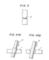
- Fig. 4(a) shows a taper joint to seal a junction between a quartz rod 9 and the flange 1 of the growth chamber. Mounting and demounting of the junction can be done from outside, so that the destruction of the rod due to the different thermal expansion of the rod and the flange material can be avoided.
- Fig. 4(b) shows another example in which a junction between the quartz rod 9 and the flange 1 is made by a solid sealing material. In these examples, a pressure necessary to make the junction tight can be applied by a screw mechanism (not shown) which is disposed on the outer chamber.
- a growing crystal and a crucible are turned in the desired directions and are moved in the longitudinal direction by shaft transmissions with the intention of proceeding a uniform crystal growth.
- Two seals for these turning shafts disposed on the flanges of the growth chamber consists of liquid B 2 0 3 .
- the rotating seal on the upper flange can be used as a pressure sensor.
- arsenic pressure in the growth chamber becomes a little higher than that outside the chamber, arsenic gas bubbles are formed at the narrow gap in the rotating seal.
- pressure balancing is attained by increasing the pressure outside the chamber so as to kill the bubbles.
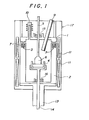
- Fig. 1 shows an embodiment of a crystal pulling apparatus in which a crystal is pulled in a sealed chamber.
- the chamber is divided into two parts 1 and 2 and the divided portions of the sealed chamber are sealed with liquid B 2 0 3 .
- the sealed chamber has two rotating seals 15 and 16 which consist of liquid B 2 0 3 .
- An upper flange 1, made of gas-tight carbon, and a lower chamber portion 2, made of gas-tight carbon, are jointed to each other by immersing the lower end portion of the upper flange 1 into the liquid B 2 0 3 7 in a groove 3.
- An expansion margin is carefully taken in the sealing portion 3 when the lower chamber portion 2 is lifted up by a driving shaft 13 which is linked with a chamber-driving mechanism (not shown).
- An optical window 9 is made of a quartz rod and a taper joint shown in Fig. 4(a) is adopted to make a seal between the optical window 9 and the upper flange portion 1.
- the temperature at the inner front of the window is maintained at an appropriate temperature between 610°C and 950°C.
- a projected portion 10 disposed on the upper flange 1 is an arsenic pressure controlling furnace.
- Reference numeral 11 represents a heater.
- Fig. 2 shows another embodiment of a crystal pulling apparatus in which a crystal is pulled in a sealed chamber.
- the chamber is divided into two portions 1 and 2 and the divided portions of the chamber are sealed with liquid B 2 0 3 .
- the chamber has two rotating seals 15 and 16 which consist of liquid B 2 0 3 .
- An upper flange 1, made of molybdenum, and a lower chamber portion 2, made of alumina, are jointed to each other by placing liquid B 2 0 3 7 in a groove 3 formed in the uppermost part of the lower chamber portion 2 and by immersing the lower end of the upper flange 1 into the sealing liquid.
- a spring 8 is inserted in the middle of the driving shaft 13 which is linked with a chamber-driving mechanism (not shown).
- the spring constant is chosen so as to apply a pressure of 20 - 30 kg/cm 2 to the contact portion between the upper flange 1 and the lower chamber portion 2.
- the spring 8 uniform and close contact of the divided chamber portions 1 and 2 is facilitated.
- a thermal expansion margin can be taken automatically with the sealed chamber even after the close contact of the divided chamber portions is completed.
- the pressure applied to the wall of the sealed chamber can be maintained in a sufficiently safe range by the spring 8 having an appropriate spring constant.
- reference numeral 9 represents an optical window made of quartz.
- the temperature at the inner front of the window is maintained at an appropriate temperature between 610°C and 950°C. Through this window the growing state of the single crystal in the chamber can be observed from outside.
- a projected part 10 on the upper flange is an arsenic pressure controlling furnace and reference numeral 11 represents a heater.
- a GaAs single crystal 6 was grown by pulling and turning the seed shaft 5 in accordance with the Czochralski method. Owing to a coil spring 8, the growth chamber was not destructed in spite of the thermal stress caused thereto by the heating-up process. The operation of balancing pressure across the chamber-wall became much easier than in the case of the apparatus shown in Fig. I., This is because the pressure difference across the growth chamber did not cause any immediate overflow of B 2 0 3 in the groove 3 due to the close contact of the divided portions of the growth chamber. The arsenic loss during the whole pulling operation was not more than 1 % of the source material. No blur was formed on the optical window 8.
- Fig. 3 shows a modified joint portion of the embodiment shown in Fig. 2 of an apparatus for growing single crystals of dissociative compounds according to the present invention, in which a solid sealing material 12 is employed for sealing the joint portion.
- a solid sealing material 12 As the solid sealing material 12, an expanded graphite plate is employed, which is flexible and free from reaction with As Gas at high temperatures and shows high sealing performance.
- a chamber driving mechanism (not shown) having the previously mentioned spring 8 as a stress-relaxation mechanism is employed for resiliently supporting the lower chamber portion 2 thereon, so that appropriate pressure is always exerted uniformly to the solid sealing material 12, whereby the destruction of the sealed chamber by its thermal expansion is avoided.
- the contact area of the two chamber-portions 1 and 2 be made small in order that the pressure applied to the chamber be effectively applied to the contact area.
- the lower end of the upper flange is made round in shape as shown in Fig. 3.
- GaAs was taken as a representative dissociative compound.
- the present invention is not limited to GaAs.
- Other dissociative compounds for instance, As compounds such as InAs, and P compounds such as InP or GaP, can also be employed.
- the sealed chamber for containing the volatile component gas is constructed so as to be capable of being divided and sealed, whereby a grown crystal is easily taken out and the growth chamber can be used repeatedly. Further, by pressing the joint containing a solid or liquid sealing material in the divided portion of the sealed chamber, highly close contact of the joint portions is attained, whereby the operation for balancing the pressure across the chamber wall is significantly improved and the arsenic dissociative loss can be extraordinarily reduced.
- the apparatus according to the present invention is made of materials sufficiently strong, at high temperatures at which single crystals are grown, highly resistive against the volatile component gas atmosphere, and can be used in repetition. Thus, single crystals of semi-conducting dissociative compounds with low dislocation density can be constantly obtained by the present invention.
Landscapes
- Chemical & Material Sciences (AREA)
- Engineering & Computer Science (AREA)
- Crystallography & Structural Chemistry (AREA)
- Materials Engineering (AREA)
- Metallurgy (AREA)
- Organic Chemistry (AREA)
- Inorganic Chemistry (AREA)
- Crystals, And After-Treatments Of Crystals (AREA)
- Liquid Deposition Of Substances Of Which Semiconductor Devices Are Composed (AREA)
Abstract
Description
- The present invention relates to an apparatus for growing single crystals of dissociative semi-conducting compounds such as GaAs, InAs, GaP and InP, which are suitable for the production of the substrates of IC devices and optical devices.
- In the production of single crystals of dissociative compounds, it is important to control the stoichiometry of the single crystals. If there is some deviation in the stoichiometry in the melt material for producing a single crystal, point defects are introduced into the crystal. The point defects aggregate and grow to dislocation loops in the crystal. Furthermore, the point defects may possibly reduce the resistance against plastic deformation of the crystal and also increase the dislocation density. It is known that the thus formed lattice defects have significant adverse effects, for instance, on the performance of IC devices using such single crystals. In order to most appropriately control the stoichiometry of the melt materials for producing a single crystal, it is considered to be effective to grow the single crystal, with the melt equilibrated with a volatile component gas at an optimum pressure. For an apparatus employed for this purpose, a technique of sealing the volatile component gas at high temperatures is supremely important. By taking as an example a dissociative compound, GaAs, the importance of the technique will now be explained. Conventionally, a GaAs single crystal is produced by Horizontal Bridgman Method (hereinafter referred to as the HB method) or by Liquid Encapsulated Czochralski method (hereinafter referred to as the LEC method). These conventional methods, however, have the following shortcomings and cannot sufficiently meet the following requirements. For instance, round semi-insulating wafers with (100) surfaces are required for use in IC substrates. The HB method in which a single crystal is grown in a boat with the GaAs melt equilibrated with an arsenic gas has the advantage that the defect density may be controlled. However, it has the shortcoming that since an ingot with a <111> direction is grown in a quartz boat in the method, the ingot must be cut into a wafer at an angle of 54.7° with respect to the growing direction of the crystal and then the wafer must be cut out into a round shape. These processes are not only extra ones to be removed, but also can cause an inhomogeneity of impurities and defects within the wafer. Furthermore, in the HB method, a quartz ampule containing the boat must be sealed by welding before the growth process and it must be then cut again in order to take out the crystal therefrom.
- In the LEC method, however, in order to avoid dissociative loss of As, the entire surface of the GaAs melt in a crucible is sealed with a B203 liquid. In this method, it is difficult to optimize the crystal growth so as to minimize the density of point defects. In other words, because the fraction of the constituent elements is decided by the composition of the source material synthesized, precise control of the melt stoichiometry during the crystal growth is impossible, so that a number of point defects are apt to be introduced into the crystal due to the non-stoichiometry. The inhomogeneity of the defect density is inevitable in the growth direction. Furthermore, in this method, the temperature gradient near the liquid-solid interface cannot be reduced significantly, since the dissociative loss of As from the crystal surface takes place. For this reason, the dislocation density increases due to the thermal strain during the cooling process.
- In order to eliminate the shortcomings of these conventional methods, it is necessary to adopt a pulling method which allows a single crystal to grow in a <100> direction at a controlled arsenic pressure. Methods to pull single crystals in a sealed chamber were reported by P. C. Leung and W. P. Allred in the Journal of Crystal Growth, Vol. 19 (1973), pages 356-358, by M. Moulin, M. Faure and G. Bichon in the Journal of Crystal Growth 24/25 (1974), pages 376-379 and by J. B. Mullin, W. R. Macewan, C. H. Holliday and A. E. V. Webb in the Journal of Crystal Growth 13/14 (1972), pages 629-634. The method in the first report, however, has the shortcoming that a growth chamber, in which an arsenic gas is sealed, must be cut after the growth process in order to take out the crystal therefrom as in the HB method. In the method described in the second and third reports, the growth chamber can be divided at a taper joint. However, a tight taper joint, if it is applied to a seal portion with a large diameter, the joint will become very difficult to divide again. Furthermore, since the growth chambers in the above reports are made of quartz which is softened when heated to 1240°C (the melting point of GaAs), the chamber may be unfavorably deformed if the - pressure difference becomes large across the chamber wall. The above-mentioned shortcomings make it difficult to scale up the size of the growth chamber so as to produce single crystals with a large diameter.
- It seems that these shortcomings hindered these apparatus from being developed to an industrial one, although these methods had-the advantage over the LEC method.
- Thus, there is a strong industrial demand for development of a crystal pulling apparatus which is capable of growing single crystals, semi-insulating or conductive and with a large diameter, at a controlled arsenic pressure. Such an apparatus should have a growth chamber with the following features:
- (1) It can retain its mechanical strength and gas- tightness at temperatures as high as 1300°C in a volatile component gas atmosphere.
- (2) It can be divided without destruction and the divided portion of the chamber can be sealed tightly without difficulty, so that the chamber can be used repeatedly.
- (3) It has an optical window through which the growing state of the crystal can be observed from outside during the course of the growth.
- (4) It has rotating seals through which rotation is transmitted to the growing crystal and the crucible.
- (5) It has a particular portion whose temperature is kept not only constant, but also lowest in the whole chamber-wall so that the arsenic pressure in the chamber may be controlled by the temperature of the particular portion.
- It is therefore an object of the present invention to provide an apparatus suitable for growing single crystals of dissociative compounds, with a volatile component gas sealed at a controlled pressure in a chamber in which a single crystal is pulled, wherein the chamber is made of one or more materials selected from the group consisting of ceramics, gas-tight carbon, heat-resistant metallic materials, ceramic-coated carbon, ceramic-coated heat-resistant metallic materials, ceramic-coated stainless steel, ceramic-coated nickel-based alloys and ceramic-coated cobalt-based alloys, the chamber can be divided and has a structure that the divided portions of the chamber can be sealed tightly, and an optical window is provided in the chamber through which the growing state of the crystal in the chamber can be observed.
- Another object of the present invention is to provide an apparatus of the above type in which a solid or liquid sealing material or a combination of such sealing materials is applied to the joint of the divided portions of the apparatus and in order to exert a pressure to the joint, a pressure application mechanism for pushing one of the divided parts of the chamber is attached to the apparatus.
- In the drawings,
- Fig. 1 shows a schematic cross-sectional view of an embodiment of an apparatus for growing single crystals of dissociative compounds according to the present invention.
- Fig. 2 shows a schematic cross-sectional view of an embodiment of an apparatus for growing single crystals of dissociative compounds according to the present invention with a coil spring inserted in a chamber-driving shaft.
- Fig. 3 shows a modified joint portion for the apparatus shown in Fig. 2 according to the present invention.
- Fig. 4(a) and Fig. 4(b) show preferred sealing methods of an optical window disposed on the flange of the growth chamber.
- A growth chamber in the present invention can be made of one or more materials selected from the following groups (A) through (D):
- (A) Ceramics (silicon carbide, silicon nitride, SIALON, boron nitride, aluminum nitride, alumina, zirconia, titanium carbide and titanium nitride)
- (B) Gas-tight carbon
- (C) Heat-resistant metallic materials (molybdenum, molybdenum alloys, tungsten and tungsten alloys)
- (D) Ceramic-coated carbon and ceramic-coated heat-resistant metallic materials including molybdenum, molybdenum alloys, tungsten, tungsten alloys, stainless steel, nickel-based alloys and cobalt-based alloys.
- In order to select the above materials, the following tests were carried out:
- Each test piece was placed in an As atmosphere at a pressure of 1 atm and at temperatures ranging from 600°C to 1250°C for about 20 hours.
- In this test, for instance, a heat-resistant steel (K-63), a cobalt-based alloy (HS 25) and a nickel-based alloy (Hastelloy) which are well-known as heat-resistant materials were easily attacked by the As atmosphere when they were in an untreated state, and were found unsuitable for use in the present invention. In contrast, the above test indicated that the above-listed materials were all suitable for use in the present invention. For instance, the above-mentioned ceramic materials are highly resistant against the As atmosphere at high temperatures and also resistant against creep, although they are difficult to process it in a fine design. Therefore, the ceramic materials are most suitable for making a pipe-formed part of the chamber which are subjected to extremely high temperatures and can be made in a simple design. On the other hand, the heat-resistant metals and ceramic-coated metals are less resistant against the arsenic atmosphere at high temperatures. However, they can easily be processed in a fine design. Therefore, those materials are suitable for making the upper and lower flanges of the chamber.
- The above materials were subjected to tests similar to the above, using phosphorus, another volatile element, instead of arsenic. The tests also indicated that the above materials can be used in a phosphorus atmosphere.
- The growth chamber is constructed.in such a way that it can be divided into two parts or more.
- To make the junction tight for the divided portions, liquid sealing materials such as B203 and Ga can be employed. Since Ga reacts with a volatile component gas at high temperatures to form a compound layer (for instance, in the case of As gas, GaAs is formed by the reaction),,H203 is more suitable than Ga for repeated use of the sealing material.
- Solid sealing materials such as an expanded graphite gasket can be advantageously applied to sealing portions, because it needs only a simple joint structure which can be formed with any chamber material listed above. The sealing operation with the solid sealing material becomes easier than in the case of the liquid sealing material which may be overflowed by large pressure difference across the chamber-wall. Furthermore, changing procedure of the sealing material becomes easier.
- It is also possible to use a solid sealing material and a liquid sealing material in combination. For instance, sealing can be performed by a solid sealing material immersed in a liquid sealing material. In this case, sealing becomes more tight and at the same time, the growth process becomes free from contamination by impurities from the solid sealing material.
- Furthermore, the apparatus is equipped with a mechanism for applying appropriate pressure to the joint of the divided portion. The object of this mechanism is firstly to exert pressure to the joint in order to make the joint tight in the case of the solid sealing material or to make the joint close enough in the case of the liquid sealing material so as to prevent the liquid to flow rapidly out of the joint portion due to the pressure difference across the chamber wall. This mechanism is secondly for preventing the chamber from being broken by the thermal expansion of the chamber itself.
- An example of such mechanism is a pushing-up mechanism including a spring suspension by which the lower portion of the chamber is resiliently supported. The object of the machanism can be attained by using a spring having appropriate strength and by detecting the reduced length of the spring so as to apply appropriate pressure to the joint. Alternatively, the pressure to the joint can be automatically controlled by using a load cell instead of the spring.
- Because the chamber is made of opaque materials, a specially disposed optical window is necessary in order to observe the growing state of the crystal in the chamber. The optical window is of a rod or a plate shape of an optically transparent material like quartz, sealed to the growth chamber by a taper joint, or a gasket.
- Fig. 4(a) shows a taper joint to seal a junction between a
quartz rod 9 and the flange 1 of the growth chamber. Mounting and demounting of the junction can be done from outside, so that the destruction of the rod due to the different thermal expansion of the rod and the flange material can be avoided. Fig. 4(b) shows another example in which a junction between thequartz rod 9 and the flange 1 is made by a solid sealing material. In these examples, a pressure necessary to make the junction tight can be applied by a screw mechanism (not shown) which is disposed on the outer chamber. - A growing crystal and a crucible are turned in the desired directions and are moved in the longitudinal direction by shaft transmissions with the intention of proceeding a uniform crystal growth. Two seals for these turning shafts disposed on the flanges of the growth chamber consists of liquid B203. The rotating seal on the upper flange can be used as a pressure sensor. In the arsenic pressure in the growth chamber becomes a little higher than that outside the chamber, arsenic gas bubbles are formed at the narrow gap in the rotating seal. Thus, pressure balancing is attained by increasing the pressure outside the chamber so as to kill the bubbles.
- Embodiments of an apparatus for growing single crystals of dissociative compounds according to the present invention will now be explained by referring to the accompanying drawings. Fig. 1 shows an embodiment of a crystal pulling apparatus in which a crystal is pulled in a sealed chamber. The chamber is divided into two
parts 1 and 2 and the divided portions of the sealed chamber are sealed with liquid B203. The sealed chamber has tworotating seals lower chamber portion 2, made of gas-tight carbon, are jointed to each other by immersing the lower end portion of the upper flange 1 into the liquid B203 7 in agroove 3. To prevent the growth chamber from being destructed due to the thermal expansion of the chamber itself, an expansion margin is carefully taken in the sealingportion 3 when thelower chamber portion 2 is lifted up by a drivingshaft 13 which is linked with a chamber-driving mechanism (not shown). Anoptical window 9 is made of a quartz rod and a taper joint shown in Fig. 4(a) is adopted to make a seal between theoptical window 9 and the upper flange portion 1. The temperature at the inner front of the window is maintained at an appropriate temperature between 610°C and 950°C. A projectedportion 10 disposed on the upper flange 1 is an arsenic pressure controlling furnace. Reference numeral 11 represents a heater. - In order to produce a GaAs single'crystal using the apparatus shown in Fig. 1, 2 kg of pre-synthesized GaAs, 15 g of surplus As and 0.6 g of Si were charged into a Si02 crucible 4. After the
whole apparatus 17 was evacuated and the B203 in thegroove 3 was melted by heating it up to about 450°C, the growth chamber was sealed by pushing thelower chamber portion 2 upwards. The As pressure in the growth chamber was maintained at a desired pressure by controlling the temperature of the Aspressure controlling furnace 10, while the crucible was heated so as to melt the source GaAs. Thecrucible 4 was rotated by ashaft 14 extending through arotating seal 16. Thereafter, a GaAssingle crystal 6 was grown by pulling and rotating theseed shaft 5 in accordance with the Czochralski method. - Fig. 2 shows another embodiment of a crystal pulling apparatus in which a crystal is pulled in a sealed chamber. The chamber is divided into two
portions 1 and 2 and the divided portions of the chamber are sealed with liquid B203. The chamber has tworotating seals lower chamber portion 2, made of alumina, are jointed to each other by placing liquid B203 7 in agroove 3 formed in the uppermost part of thelower chamber portion 2 and by immersing the lower end of the upper flange 1 into the sealing liquid. Aspring 8 is inserted in the middle of the drivingshaft 13 which is linked with a chamber-driving mechanism (not shown). The spring constant is chosen so as to apply a pressure of 20 - 30 kg/cm2 to the contact portion between the upper flange 1 and thelower chamber portion 2. By thespring 8, uniform and close contact of the dividedchamber portions 1 and 2 is facilitated. Furthermore, a thermal expansion margin can be taken automatically with the sealed chamber even after the close contact of the divided chamber portions is completed. In other words, the pressure applied to the wall of the sealed chamber can be maintained in a sufficiently safe range by thespring 8 having an appropriate spring constant. - In the figure,
reference numeral 9 represents an optical window made of quartz. The temperature at the inner front of the window is maintained at an appropriate temperature between 610°C and 950°C. Through this window the growing state of the single crystal in the chamber can be observed from outside. A projectedpart 10 on the upper flange is an arsenic pressure controlling furnace and reference numeral 11 represents a heater. - In order to produce a GaAs single crystal using the apparatus shown in figure 2, 1 kg of a mixture of Ga and As was charged into a
PBN crucible 4. After thewhole apparatus 17 was entirely evacuated and the B203 in thegroove 3 was melted by heating it up to about 450°C, the growth chamber was sealed by pushing up thelower chamber portion 2. The As pressure in the growth chamber was maintained at a desired pressure by controlling the temperature of an Aspressure controlling furnace 10. GaAs was then directly synthesized in the sealed chamber by heating the crucible up to 1240°C by the heater 11. Thecrucible 4 was rotated by ashaft 14 extending through arotating seal 16. Thereafter, a GaAssingle crystal 6 was grown by pulling and turning theseed shaft 5 in accordance with the Czochralski method. Owing to acoil spring 8, the growth chamber was not destructed in spite of the thermal stress caused thereto by the heating-up process. The operation of balancing pressure across the chamber-wall became much easier than in the case of the apparatus shown in Fig. I., This is because the pressure difference across the growth chamber did not cause any immediate overflow of B203 in thegroove 3 due to the close contact of the divided portions of the growth chamber. The arsenic loss during the whole pulling operation was not more than 1 % of the source material. No blur was formed on theoptical window 8. - Fig. 3 shows a modified joint portion of the embodiment shown in Fig. 2 of an apparatus for growing single crystals of dissociative compounds according to the present invention, in which a
solid sealing material 12 is employed for sealing the joint portion. As thesolid sealing material 12, an expanded graphite plate is employed, which is flexible and free from reaction with As Gas at high temperatures and shows high sealing performance. To make the seal tight, a chamber driving mechanism (not shown) having the previously mentionedspring 8 as a stress-relaxation mechanism is employed for resiliently supporting thelower chamber portion 2 thereon, so that appropriate pressure is always exerted uniformly to thesolid sealing material 12, whereby the destruction of the sealed chamber by its thermal expansion is avoided. It is preferable that the contact area of the two chamber-portions 1 and 2 be made small in order that the pressure applied to the chamber be effectively applied to the contact area. For this purpose, the lower end of the upper flange is made round in shape as shown in Fig. 3. - By applying the solid sealing material with an appropriate pressure exerted thereon, a tight seal of the divided chamber portions was realized and both the operation of balancing pressure across the chamber-wall during the growth process and the maintenance of the sealing material became significantly easier.
- In the above described embodiments, GaAs was taken as a representative dissociative compound. However, the present invention is not limited to GaAs. Other dissociative compounds, for instance, As compounds such as InAs, and P compounds such as InP or GaP, can also be employed.
- In the present invention, the sealed chamber for containing the volatile component gas is constructed so as to be capable of being divided and sealed, whereby a grown crystal is easily taken out and the growth chamber can be used repeatedly. Further, by pressing the joint containing a solid or liquid sealing material in the divided portion of the sealed chamber, highly close contact of the joint portions is attained, whereby the operation for balancing the pressure across the chamber wall is significantly improved and the arsenic dissociative loss can be extraordinarily reduced. The apparatus according to the present invention is made of materials sufficiently strong, at high temperatures at which single crystals are grown, highly resistive against the volatile component gas atmosphere, and can be used in repetition. Thus, single crystals of semi-conducting dissociative compounds with low dislocation density can be constantly obtained by the present invention.
Claims (2)
Applications Claiming Priority (4)
| Application Number | Priority Date | Filing Date | Title |
|---|---|---|---|
| JP157883/83 | 1983-08-31 | ||
| JP15788383A JPS6051698A (en) | 1983-08-31 | 1983-08-31 | Arsenic compound single crystal growing apparatus |
| JP10963284A JPS60255692A (en) | 1984-05-31 | 1984-05-31 | Apparatus for treating compound semiconductor single crystal having high dissociation pressure |
| JP109632/84 | 1984-05-31 |
Publications (2)
| Publication Number | Publication Date |
|---|---|
| EP0139157A1 true EP0139157A1 (en) | 1985-05-02 |
| EP0139157B1 EP0139157B1 (en) | 1988-07-06 |
Family
ID=26449368
Family Applications (1)
| Application Number | Title | Priority Date | Filing Date |
|---|---|---|---|
| EP84109948A Expired EP0139157B1 (en) | 1983-08-31 | 1984-08-21 | Apparatus for growing single crystals of dissociative compounds |
Country Status (3)
| Country | Link |
|---|---|
| US (1) | US4704257A (en) |
| EP (1) | EP0139157B1 (en) |
| DE (2) | DE139157T1 (en) |
Cited By (6)
| Publication number | Priority date | Publication date | Assignee | Title |
|---|---|---|---|---|
| EP0146002A3 (en) * | 1983-11-22 | 1985-12-27 | Sumitomo Electric Industries Limited | Apparatus for production of a single crystal and monitoring of the production |
| EP0174060A1 (en) * | 1984-06-08 | 1986-03-12 | Sumitomo Electric Industries Limited | Method for growing a single crystal |
| EP0355746A3 (en) * | 1988-08-19 | 1991-07-03 | Mitsubishi Materials Corporation | Method for monocrystalline growth of dissociative compound semiconductors |
| EP0355747A3 (en) * | 1988-08-19 | 1991-07-03 | Mitsubishi Materials Corporation | Method for monocrystalline growth of dissociative compound semiconductors |
| EP0559921A4 (en) * | 1991-09-19 | 1995-11-22 | Mitsubishi Materials Corp | Apparatus for and method of producing single crystal semiconductor of high dissociation pressure compound |
| EP1247882A1 (en) * | 2001-04-06 | 2002-10-09 | General Research Institute for Nonferrous Metals | Vapor controlled czochralski (VCZ) single crystal growth apparatus |
Families Citing this family (15)
| Publication number | Priority date | Publication date | Assignee | Title |
|---|---|---|---|---|
| US4936947A (en) * | 1987-05-05 | 1990-06-26 | Mobil Solar Energy Corporation | System for controlling apparatus for growing tubular crystalline bodies |
| USRE34375E (en) * | 1987-05-05 | 1993-09-14 | Mobil Solar Energy Corporation | System for controlling apparatus for growing tubular crystalline bodies |
| US5264189A (en) * | 1988-02-23 | 1993-11-23 | Mitsubishi Materials Corporation | Apparatus for growing silicon crystals |
| KR0140210B1 (en) * | 1989-03-30 | 1998-06-01 | 추네오 나카하라 | Sintering furnace for producing quartz base material |
| WO1998035074A1 (en) * | 1997-02-06 | 1998-08-13 | Crysteco, Inc. | Method and apparatus for growing crystals |
| US6019841A (en) * | 1997-03-24 | 2000-02-01 | G.T. Equuipment Technologies Inc. | Method and apparatus for synthesis and growth of semiconductor crystals |
| JP4135239B2 (en) * | 1997-12-26 | 2008-08-20 | 住友電気工業株式会社 | Semiconductor crystal, manufacturing method thereof and manufacturing apparatus |
| US6572700B2 (en) * | 1997-12-26 | 2003-06-03 | Sumitomo Electric Industries, Ltd. | Semiconductor crystal, and method and apparatus of production thereof |
| JP2003124235A (en) * | 2001-10-17 | 2003-04-25 | Sumitomo Electric Ind Ltd | II-VI compound semiconductor, heat treatment method therefor and heat treatment apparatus therefor |
| DE10204468C1 (en) * | 2002-02-05 | 2003-06-18 | Sgl Carbon Ag | Highly pure replaceable wear insert production from expanded graphite, used as insert for semiconductor manufacturing crucible comprises placing expanded graphite into pressing mold and subjecting to pressure |
| US7604240B2 (en) * | 2002-09-16 | 2009-10-20 | Hewlett-Packard Development Company, L.P. | Capillary seal for a burn chamber |
| DE102006002682A1 (en) * | 2006-01-19 | 2007-08-02 | Siltronic Ag | Apparatus and method for producing a single crystal, single crystal and semiconductor wafer |
| CN113308740B (en) * | 2021-06-03 | 2022-06-24 | 中国电子科技集团公司第十三研究所 | Preparation method of semi-insulating indium phosphide |
| US12559861B2 (en) | 2021-06-03 | 2026-02-24 | The 13Th Research Institute Of China Electronics Technology Group Corporation | Preparation device and method for semi-insulating indium phosphide |
| CN114688250B (en) * | 2022-04-19 | 2024-09-13 | 北京通美晶体技术股份有限公司 | Novel sealing structure for gallium arsenide crystal growth |
Family Cites Families (10)
| Publication number | Priority date | Publication date | Assignee | Title |
|---|---|---|---|---|
| US412702A (en) * | 1889-10-08 | Half to wilhelm thomas | ||
| US1646325A (en) * | 1924-05-31 | 1927-10-18 | Strassmann Paul Gerhard | Closure for vertical retorts |
| US2311349A (en) * | 1941-04-19 | 1943-02-16 | Puening Franz | Coke oven with movable walls |
| GB1113069A (en) * | 1964-07-29 | 1968-05-08 | Nat Res Dev | Crystalline material |
| NL6917398A (en) * | 1969-03-18 | 1970-09-22 | ||
| US3647389A (en) * | 1970-05-11 | 1972-03-07 | Bell Telephone Labor Inc | Method of group iii-v semiconductor crystal growth using getter dried boric oxide encapsulant |
| US3857679A (en) * | 1973-02-05 | 1974-12-31 | Univ Southern California | Crystal grower |
| DE2349736A1 (en) * | 1973-10-03 | 1975-04-24 | Siemens Ag | MONITORING DEVICE FOR A DEVICE FOR PULLING CRYSTALS FROM THE MELT |
| JPS5326280A (en) * | 1976-08-24 | 1978-03-10 | Handotai Kenkyu Shinkokai | Crystal growth for mixed crystals of compund semiconductor |
| DE3466785D1 (en) * | 1983-08-06 | 1987-11-19 | Sumitomo Electric Industries | Apparatus for the growth of single crystals |
-
1984
- 1984-08-21 EP EP84109948A patent/EP0139157B1/en not_active Expired
- 1984-08-21 DE DE198484109948T patent/DE139157T1/en active Pending
- 1984-08-21 DE DE8484109948T patent/DE3472577D1/en not_active Expired
- 1984-08-28 US US06/644,840 patent/US4704257A/en not_active Expired - Lifetime
Non-Patent Citations (2)
| Title |
|---|
| PATENTS ABSTRACTS OF JAPAN, vol. 3, no. 147(C-66), 5th December 1979, page 22C66; & JP - A - 54 123 585 (MITSUBISHI KINZOKU K.K.) 25-09-1979 * |
| PATENTS ABSTRACTS OF JAPAN, vol. 7, no. 201(C-184)(1346), 6th September 1983; & JP - A - 58 99195 (MITSUBISHI KINZOKU K.K.) 13-06-1983 * |
Cited By (6)
| Publication number | Priority date | Publication date | Assignee | Title |
|---|---|---|---|---|
| EP0146002A3 (en) * | 1983-11-22 | 1985-12-27 | Sumitomo Electric Industries Limited | Apparatus for production of a single crystal and monitoring of the production |
| EP0174060A1 (en) * | 1984-06-08 | 1986-03-12 | Sumitomo Electric Industries Limited | Method for growing a single crystal |
| EP0355746A3 (en) * | 1988-08-19 | 1991-07-03 | Mitsubishi Materials Corporation | Method for monocrystalline growth of dissociative compound semiconductors |
| EP0355747A3 (en) * | 1988-08-19 | 1991-07-03 | Mitsubishi Materials Corporation | Method for monocrystalline growth of dissociative compound semiconductors |
| EP0559921A4 (en) * | 1991-09-19 | 1995-11-22 | Mitsubishi Materials Corp | Apparatus for and method of producing single crystal semiconductor of high dissociation pressure compound |
| EP1247882A1 (en) * | 2001-04-06 | 2002-10-09 | General Research Institute for Nonferrous Metals | Vapor controlled czochralski (VCZ) single crystal growth apparatus |
Also Published As
| Publication number | Publication date |
|---|---|
| EP0139157B1 (en) | 1988-07-06 |
| US4704257A (en) | 1987-11-03 |
| DE3472577D1 (en) | 1988-08-11 |
| DE139157T1 (en) | 1985-11-07 |
Similar Documents
| Publication | Publication Date | Title |
|---|---|---|
| EP0139157B1 (en) | Apparatus for growing single crystals of dissociative compounds | |
| JP3491402B2 (en) | Single crystal manufacturing method and single crystal manufacturing apparatus | |
| EP0140509A1 (en) | An lec method and apparatus for growing single crystal | |
| US5047113A (en) | Method for directional solidification of single crystals | |
| Capper | Bulk crystal growth: methods and materials | |
| CA2478894A1 (en) | Apparatus for growing monocrystalline group ii-vi and iii-v compounds | |
| EP0162467B1 (en) | Device for growing single crystals of dissociative compounds | |
| US4944925A (en) | Apparatus for producing single crystals | |
| Trivich et al. | Preparation of Single Crystals of Cuprous Oxide in an Arc‐Image Furnace | |
| JPS6341879B2 (en) | ||
| EP0355833B1 (en) | Method of producing compound semiconductor single crystal | |
| WO2019053856A1 (en) | Gallium arsenide compound semiconductor crystal and wafer group | |
| JP2723249B2 (en) | Crystal growing method and crucible for crystal growing | |
| JP2734820B2 (en) | Method for manufacturing compound semiconductor single crystal | |
| JP2690420B2 (en) | Single crystal manufacturing equipment | |
| JP2612897B2 (en) | Single crystal growing equipment | |
| JP2576239B2 (en) | Compound semiconductor crystal growth equipment | |
| JP2611336B2 (en) | High dissociation pressure compound semiconductor processing equipment | |
| Austerman | Flux process for growth of large crystals with application to beryllia | |
| JP3938674B2 (en) | Method for producing compound semiconductor single crystal | |
| JPH0952789A (en) | Production of single crystal | |
| JPH0558772A (en) | Method for producing compound semiconductor single crystal | |
| JP2710429B2 (en) | High dissociation pressure compound semiconductor processing equipment | |
| JPH10182277A (en) | Single crystal manufacturing apparatus and single crystal manufacturing method using the same | |
| JPS6348837B2 (en) |
Legal Events
| Date | Code | Title | Description |
|---|---|---|---|
| PUAI | Public reference made under article 153(3) epc to a published international application that has entered the european phase |
Free format text: ORIGINAL CODE: 0009012 |
|
| AK | Designated contracting states |
Designated state(s): DE FR GB |
|
| EL | Fr: translation of claims filed | ||
| 17P | Request for examination filed |
Effective date: 19850808 |
|
| DET | De: translation of patent claims | ||
| 17Q | First examination report despatched |
Effective date: 19860613 |
|
| D17Q | First examination report despatched (deleted) | ||
| RAP1 | Party data changed (applicant data changed or rights of an application transferred) |
Owner name: MITSUBISHI METAL CORPORATION Owner name: RESEARCH DEVELOPMENT CORPORATION OF JAPAN |
|
| GRAA | (expected) grant |
Free format text: ORIGINAL CODE: 0009210 |
|
| AK | Designated contracting states |
Kind code of ref document: B1 Designated state(s): DE FR GB |
|
| REF | Corresponds to: |
Ref document number: 3472577 Country of ref document: DE Date of ref document: 19880811 |
|
| ET | Fr: translation filed | ||
| PLBE | No opposition filed within time limit |
Free format text: ORIGINAL CODE: 0009261 |
|
| STAA | Information on the status of an ep patent application or granted ep patent |
Free format text: STATUS: NO OPPOSITION FILED WITHIN TIME LIMIT |
|
| 26N | No opposition filed | ||
| REG | Reference to a national code |
Ref country code: FR Ref legal event code: CD Ref country code: FR Ref legal event code: CA |
|
| PGFP | Annual fee paid to national office [announced via postgrant information from national office to epo] |
Ref country code: GB Payment date: 19950731 Year of fee payment: 12 |
|
| PGFP | Annual fee paid to national office [announced via postgrant information from national office to epo] |
Ref country code: FR Payment date: 19950817 Year of fee payment: 12 |
|
| PGFP | Annual fee paid to national office [announced via postgrant information from national office to epo] |
Ref country code: DE Payment date: 19950928 Year of fee payment: 12 |
|
| PG25 | Lapsed in a contracting state [announced via postgrant information from national office to epo] |
Ref country code: GB Effective date: 19960821 |
|
| GBPC | Gb: european patent ceased through non-payment of renewal fee |
Effective date: 19960821 |
|
| PG25 | Lapsed in a contracting state [announced via postgrant information from national office to epo] |
Ref country code: FR Effective date: 19970430 |
|
| PG25 | Lapsed in a contracting state [announced via postgrant information from national office to epo] |
Ref country code: DE Effective date: 19970501 |
|
| REG | Reference to a national code |
Ref country code: FR Ref legal event code: ST |