EP0138277A2 - Apparatus for reproducing information from an optically readable record carrier - Google Patents
Apparatus for reproducing information from an optically readable record carrier Download PDFInfo
- Publication number
- EP0138277A2 EP0138277A2 EP84201457A EP84201457A EP0138277A2 EP 0138277 A2 EP0138277 A2 EP 0138277A2 EP 84201457 A EP84201457 A EP 84201457A EP 84201457 A EP84201457 A EP 84201457A EP 0138277 A2 EP0138277 A2 EP 0138277A2
- Authority
- EP
- European Patent Office
- Prior art keywords
- signal
- detectors
- detector
- zero
- tracking
- Prior art date
- Legal status (The legal status is an assumption and is not a legal conclusion. Google has not performed a legal analysis and makes no representation as to the accuracy of the status listed.)
- Granted
Links
Images


Classifications
-
- G—PHYSICS
- G11—INFORMATION STORAGE
- G11B—INFORMATION STORAGE BASED ON RELATIVE MOVEMENT BETWEEN RECORD CARRIER AND TRANSDUCER
- G11B7/00—Recording or reproducing by optical means, e.g. recording using a thermal beam of optical radiation by modifying optical properties or the physical structure, reproducing using an optical beam at lower power by sensing optical properties; Record carriers therefor
- G11B7/08—Disposition or mounting of heads or light sources relatively to record carriers
- G11B7/09—Disposition or mounting of heads or light sources relatively to record carriers with provision for moving the light beam or focus plane for the purpose of maintaining alignment of the light beam relative to the record carrier during transducing operation, e.g. to compensate for surface irregularities of the latter or for track following
- G11B7/095—Disposition or mounting of heads or light sources relatively to record carriers with provision for moving the light beam or focus plane for the purpose of maintaining alignment of the light beam relative to the record carrier during transducing operation, e.g. to compensate for surface irregularities of the latter or for track following specially adapted for discs, e.g. for compensation of eccentricity or wobble
-
- G—PHYSICS
- G11—INFORMATION STORAGE
- G11B—INFORMATION STORAGE BASED ON RELATIVE MOVEMENT BETWEEN RECORD CARRIER AND TRANSDUCER
- G11B7/00—Recording or reproducing by optical means, e.g. recording using a thermal beam of optical radiation by modifying optical properties or the physical structure, reproducing using an optical beam at lower power by sensing optical properties; Record carriers therefor
- G11B7/08—Disposition or mounting of heads or light sources relatively to record carriers
- G11B7/09—Disposition or mounting of heads or light sources relatively to record carriers with provision for moving the light beam or focus plane for the purpose of maintaining alignment of the light beam relative to the record carrier during transducing operation, e.g. to compensate for surface irregularities of the latter or for track following
- G11B7/0901—Disposition or mounting of heads or light sources relatively to record carriers with provision for moving the light beam or focus plane for the purpose of maintaining alignment of the light beam relative to the record carrier during transducing operation, e.g. to compensate for surface irregularities of the latter or for track following for track following only
-
- G—PHYSICS
- G11—INFORMATION STORAGE
- G11B—INFORMATION STORAGE BASED ON RELATIVE MOVEMENT BETWEEN RECORD CARRIER AND TRANSDUCER
- G11B7/00—Recording or reproducing by optical means, e.g. recording using a thermal beam of optical radiation by modifying optical properties or the physical structure, reproducing using an optical beam at lower power by sensing optical properties; Record carriers therefor
- G11B7/08—Disposition or mounting of heads or light sources relatively to record carriers
- G11B7/09—Disposition or mounting of heads or light sources relatively to record carriers with provision for moving the light beam or focus plane for the purpose of maintaining alignment of the light beam relative to the record carrier during transducing operation, e.g. to compensate for surface irregularities of the latter or for track following
Definitions
- the invention relates to an apparatus for reproducing information from an optically readable record carrier on which information is stored in the form of a track of optically detectable areas which alternate with intermediate areas, which apparatus comprises an optical system for projecting a light beam on an optical detector via the record carrier, which detector comprises four sub- detectors situated in separate quadrants of an imaginary X-Y-coordinate system whose origin is situated on the optical axis of the optical system and of which the X-axis extends effectively in the track direction and the Y-axis extends effectively transversely of the track direction, a first adder circuit for adding the signals supplied by diagonally disposed first and third sub-detectors to form a first signal, a second adder circuit for adding the signals supplied by at least the other two sub-detectors to form a second signal, and a tracking-error signal generator for driving a tracking-error signal from the first and the second signal.
- Such apparatus is known from Netherlands Patent Application no. 7600842 (PHN 8290) and may be employed in, inter alia "compact-disc digital audio" players.
- a tracking-error signal is obtained by shifting the phase of the second signal through 90 0 , multiplying said phase-shifted signal by the first signal, and subsequently passing it through a low-pass filter.
- the apparatus is characterized in that the tracking-error signal generator comprises means for measuring the time interval between corresponding zero crossings of the first and the second signal and generating a signal which depends on said time interval and forms the tracking-error signal.
- the apparatus in accordance with the invention meets the desired object because:
- An embodiment of the apparatus in accordance with the invention which is intended for reading a record carrier in which information of a substantially fixed bit frequency is stored, may be further characterized by first and second zero-crossing detectors for supplying first and second pulses respectively at the zero crossings of the first and the second signal respectively, first and second tuned circuits which are tuned to the bit frequency or upper harmonics thereof and which are excited by the first and the second zero-crossing detectors respectively, and a first phase detector for detecting the phase difference between the signals supplied by the first and the second tuned circuit.
- This embodiment may be further characterized by a third zero-crossing detector for supplying third pulses at zero crossings of the third signal, a third tuned circuit which is tuned to the bit frequency or an upper harmonic thereof, and which is excited by saif third zero-crossing detector, a second phase detector for detecting the phase difference between the signals supplied by the second and the third tuned circuits, and a summing device for adding the signals supplied by the first and the second phase detector.
- An alternative to this embodiment may be characterized in that the apparatus comprises means for generating a pulse-shaped signal of a duration corresponding to the interval between corresponding zero crossings of the first and the second signal, time-measurement means for determining the duration of the pulses of said pulse-shape signal, direction-detection means for detecting the sequence in which corresponding zero crossings of the first and the second signal occur and in response thereto inverting or not inverting the polarity of the output signal of the time-measurement means.
- this embodiment may be characterized in that the means for generating a pulse-shaped signal comprise first and second limiter means for converting the first and the second signal into a substantially rectangular signal, and a gate circuit with an exclusive-OR function to which said limited signals are applied, and with respect to the direction-detection means, in that the direction-detection means comprise a detector which determines the polarity of the first signal at the instant of a zero-crossing of the second signal.
- Fig. 1 shows a round disc-shaped record carrier 1 in radial cross-section.
- the information structure is assumed to be reflecting and comprises tracks of optically detectable areas alternating with intermediate areas.
- the information tracks bear the reference numeral 3.
- a mirror 9 reflects this beam to an objective system 11, which is schematically represented by a single lens.
- an auxiliary lens 7 is arranged, which ensures that the read beam fills the pupil of the objective system entirely.
- a radiation spot of minimal dimensions is then formed on the surface 2 of the information structure.
- the read beam is reflected by the information structure and, as the record carrier rotates about an spindle 5 which projects through a centre hole 4, this beam is time-modulated in conformity with the information stored in the track to be read.
- the modulated read beam again passes through the objective system and is reflected by the mirror 9 in the same direction as the beam emitted by the source.
- Elements for separating the paths of the modulated and the unmodulated read beams are arranged in the radiation path of the read beam. These elements may comprise, for example, an assembly of a polarization-sensitive beam-splitter prism and a /l/ 4 plate.
- the said means comprise a semi-transparent mirror 8. This mirror reflects a part of the modulated read beam to a radiation-sensitive detection system 12.
- the optical details of the information structure are very small.
- the read spot should therefore remain centred very accurately on the track to be read.
- the detection system 12 comprises, for example, four radiation-sensitive detectors, as is shown in Fig. 2.
- the four detectors 13, 14, 15 and 16 are disposed in four different quadrants of an X-Y-coordinate system.
- the longitudinal direction and the lateral direction of the track portion extend parallel to the X-axis and the Y-axis respectively.
- the output signals of the detectors 13 and 15 are added to each other by means of the adder circuit 17 and the output signals of the detectors 14 and 16 are added to each other by means of the adder circuit 18.
- the output signals S 1 and S 2 of the adder circuits 17 and 18 are subtracted from each other in the subtractor circuit 19.
- the output of this circuit is connected to one of the inputs of a multiplier circuit 22.
- the output signal of the circuit 22 is applied to a low-pass filter 23.
- the desired control signal is obtained on the output 28 of this filter.
- the output signals of the adder circuits 17 and 18 are added to each other in an adder circuit 24.
- the desired read signal then appears on the output of this adder circuit 24.
- the signal supplied by the subtractor circuit 19 which signal is the difference between the signals supplied by the two pairs of diagonally situated detectors 13, 15 and 14, 16 has a polarity which depends on the direction of the tracking error, i.e. the deviation of the spot formed by the laser beam b from the information track 3 to be followed, and varies when an optically detectable area or an intermediate area in the track 3 is scanned, the directional information is not available in the output signal of the subtractor circuit 19.
- the sum signal from the adder circuit 24 is 90° shifted in phase in the phase shifter 25 and applied to the other input of the multiplier 22, which thus operates as a synchronous detector.
- the directional information of the tracking error is then contained in said output signal as the polarity of the low-frequency component (which is passed by the filter 23).
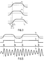
- Fig. 3 shows some waveform diagrams to illustrate the principle of the apparatus in accordance with the invention.
- the Figure shows an example of the variation of the signals S 1 , S 2 and So when an optically detectable areas passes the spot where the beam is incident.
- the signal So then intersects the zero axis at an instant t O .
- the spot formed by the beam has such a deviation from the track that the image of the optically detectable area situated above the X-axis in the Figure, assuming that owing to the displacement of the record carrier this image moves to the left in the Figure, the passage of optically detectable areas will be detected by the detectors 13 and 15 before the detectors 14 and 16, which can be seen in the diagrams of Figure 3 in that the signal S 1 intersects the zero axis at the instant t 1 , which appears a time ⁇ T before the instant t O , and in that the signal S 2 intersects the zero axis at the instant t 2 , which appears a time ⁇ T after the instant t O .
- the signal S 2 will intersect the zero axis at the instant t 1 and the signal S 1 at the instant t 2 .
- the magnitude of the time interval ⁇ T is then a measure of the deviation of this spot.
- a tracking signal can then be found by measuring said time ⁇ T, whilst it is possible to measure the time interval between the instants t 1 and t 21 i.e. between the zero crossings of the signals S 1 and S 2 or, alternatively, to measure the time interval between one of the instants t 1 and t 2 and the instant t O , i.e. between the zero crossings of the signal S or S 2 and the signal S 0 .
- Fig. 4 shows an embodiment of an apparatus in accordance with the invention which is intended in particular for use in conjunction with record carriers on which a digital signal (for example a digital audio signal) of fixed bit frequency is recorded, and in which the detectors 13 to 16 and the adder circuits 17, 24 and 18 are identical to those in Fig. 2.
- the signals S 1 , S 2 and So supplied by said adder circuits are applied to limiter circuits 30, 31 and 32 and subsequently to zero-crossing detectors 33, 34 and 35 which supply a pulse in the case of a zero crossing of their input signals, and which may comprise for example monostable multivibrators, differen- tiators and exclusive-or gates, to which the signal is applied directly and with a specific time delay.
- the zero-crossing detectors 33, 34 and 35 excite band-pass filters 36, 37 and 38 which are tuned to a frequency fo which corresponds to the bit frequency of the reproduced signal.
- the operation of this part of the apparatus shown in Fig. 4 will be described with reference to Fig.5. From top to bottom this Figure shows the signal S O on the output of the adder circuit 24, the signal S 3 on the output of the limiter circuit 31, the signal S 4 on an output of the zero-crossing detector 34, and the signal S 5 on the output of the band-pass filter 37.
- the signal S O is limited, so that a squarewave signal S 3 is obtained whose zero crossings coincide with the zero crossings of the signal S 0 .
- the signal S 4 then comprises pulses in synchronism with the zero crossings.
- the narrow-band band-pass filter 37 is then excited by these pulses. As this filter is tuned to the bit frequency of the recorded signal the pulses at the zero crossings always appear in phase with the waveform on the output of the band-pass filter 37.
- the signal S 5 is a waveform of the frequency fo, which is excited each time and whose amplitude decays after every excitation. The instants at which the zero crossings of the signal S 0 appear are then defined by the instantaneous phase of the signal S 5 .
- the band-pass filter thus functions as a hold circuit for the zero-crossing instant.
- band-pass filters 36 and 38 supply waveforms of the frequency fo. Their mutual phase relationship depends on the intervals between the zero-crossing instants of the signals S O , S 1 and S 2 and consequently on the tracking error.
- phase differences and the tracking-error signal are further determined in the same manner as in the apparatus shown in Fig. 2, but now by means of signals of constant frequency fo.
- the signals are applied to a limiter circuits 40, 41 and 42.
- the output signals of the limiter circuits 40 and 41 are applied to a multiplier 43 and the output signals of the limiter circuits 41 and 42 are applied to a multiplier 44.
- the low-frequency component of the output signal of the multiplier 43 then depends on the time interval t 1 -t O (Fig. 3) and the low-frequency component of the output signal of the multiplier 44 on the time interval t O -t 2 .
- the two output signals are added to each other in the adder 45 and subsequently they are applied to the output 28 via the low-pass filter 23.
- a disadvantage of the tracking-error detection in accordance with Fig. 4 is that the maximum time ⁇ T which can be measured unambiguously is in principle equal to one period of the waveform of the frequency fo and, as a result of the use of multipliers for the phase detectors, it is even limited to a quarter of this period.
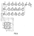
- Fig. 6 shows a second embodiment of an apparatus in accordance with the invention whose use is not limited to reading record carriers on which information of a substantially fixed bit frequency is recorded and whose measurement range is in principle equal to the length of the optically detectable area being read.
- the apparatus shown in Fig. 4 it comprises the detectors 13, 14, 15 and 16, the adder circuits 17, 18 and 24, and the limiter circuits 30, 32 and 31.
- the output signals of the limiter circuits 30 and 32 are applied to an exclusive-or gate 46. This gate then supplies an output signal during the intervals in which the output signals of the limiters 30 and 32 are of opposite polarity, i.e. during the intervals t 1 to t 2 (Fig. 3).
- the duration of the output signal of this exclusive-or gate 46 is consequently a measure of the tracking error.
- the output signal of the gate 46 closes a switch 47, so that the current from a current source 48 charges a capacitor 49.
- the charge of this capacitor after the switch 47 has been opened again is then a measure of the duration of the output signal of the gate 46 and hence a measure of the tracking error.
- Via a voltage follower 50 and a switch 51 the capacitor 49 is connected to a capacitor 52.
- the switch 51 is actuated by the output signal of a pulse shaper 53 which responds to the negative edge of the output signal of the gate 46, so that the switch 51 is closed af.,-3r switch 47 has been opened again and the capacitor 52 is charged to the value of the charge on the capacitor 49.
- the switch 51 and the capacitor 52 thus function as a hold circuit.
- a pulse shaper 54 responds to the negative edge of the output signal of the pulse shaper 53 and controls a switch 55 which is arranged in parallel with capacitor 49, so that after the charge of capacitor 49 has been detected via the switch 51, the capacitor 49 is discharged again via the switch 55.
- the charge on capacitor 52 is a measure of the tracking error. However, the direction of this tracking error is still unknown.
- the charge on capacitor 52 is applied to a switchable inverter circuit 57 via a voltage follower, so that the polarity of the signal after said switchable inverter circuit 57 is an indication of the direction of the tracking error.
- the output signal of said switchable inverter circuit is applied to an output 28 via output 28 via the low-pass filter 23.
- the output signal of the limiter 32 is applied to the D-input of a D-flip-flop 58, the output signal of the limiter 31 being applied to the clock input C.
- the flip-flop 58 is of a type which is triggered on the negative edge of the signal on its clock input C, so that the output signal of the flip-flop 58 follows the output signal of the limiter 32 at the zero-crossing instants during the negative edges of the signal S (i.e. instant t 3 in Fig. 3).
- the output signal on the Q-output of the flip-flop 58 is then high if the signal S 2 is high at the instant t 3 , or if the signal S 2 lags the signal S 0 .
- the output signal of the limiter 32 is applied to the 0-input of a D flip-flop 59 and the inverted output signal of the limiter 31 is applied to the clock input C, so that flip-flop 59 is triggered on the zero-crossings of the signal S 0 during positive edges, or at the instant to (Fig. 3).
- the inverted output Q of flip_flop 59 is then if the signal S 2 is low at the instant to or if the signal S 2 is lagging.
- the Q-output of flip-flop 58 and the Q -output of flip-flop 59 are alternately connected to the D-input of a D flip-flop 61 which is clocked by the negative edges of the output signal of the pulse shaper 53, i.e. at the same time that the switch 61 which samples the charge on the capacitor 49 is closed.
- the flip-flop 61 generates a signal of a polarity corresponding to the direction of the tracking error, which flip-flop is clocked again after every time measurement.
- the flip-flop 61 in its turn controls the switchable inverter circuit 57.
- the time interval t 1 -t 2 (Fig. 3) is measured in the similar manner.
- a digital measurement is also possible, for example in the apparatus shown in Fig. 6 by starting a counter by means of the exclusive-or gate 46, which counter counts the counting pulses supplied by a high-frequency counting- pulse oscillator.
Abstract
Description
- The invention relates to an apparatus for reproducing information from an optically readable record carrier on which information is stored in the form of a track of optically detectable areas which alternate with intermediate areas, which apparatus comprises an optical system for projecting a light beam on an optical detector via the record carrier, which detector comprises four sub- detectors situated in separate quadrants of an imaginary X-Y-coordinate system whose origin is situated on the optical axis of the optical system and of which the X-axis extends effectively in the track direction and the Y-axis extends effectively transversely of the track direction, a first adder circuit for adding the signals supplied by diagonally disposed first and third sub-detectors to form a first signal, a second adder circuit for adding the signals supplied by at least the other two sub-detectors to form a second signal, and a tracking-error signal generator for driving a tracking-error signal from the first and the second signal.
- Such apparatus is known from Netherlands Patent Application no. 7600842 (PHN 8290) and may be employed in, inter alia "compact-disc digital audio" players.
- In the known apparatus a tracking-error signal is obtained by shifting the phase of the second signal through 900, multiplying said phase-shifted signal by the first signal, and subsequently passing it through a low-pass filter. Such a method of generating the tracking error signal is found to be unsatisfactory, in particular in compact-disc players, because the 900 phase shift cannot be obtained due to the varying instantaneous frequency of the signal being read and because the generated tracking-error signal is influenced considerably by the recorded information signal.
- It is the object of the invention to provide an apparatus of the type specified in the opening paragraph which does not require a 900 phase shift of the signal being read and in which the generated tracking-error signal is more independent of the recorded information.
- According to the invention the apparatus is characterized in that the tracking-error signal generator comprises means for measuring the time interval between corresponding zero crossings of the first and the second signal and generating a signal which depends on said time interval and forms the tracking-error signal.
- The apparatus in accordance with the invention meets the desired object because:
- - it does not require a 900 phase-shift of a signal whose instantaneous frequency is not fixed,
- - said time measurement is lacked to the zero crossings of the signal being read and consequently to the instantaneous frequency of the signal being read, so that the time measurement exhibits a repetition frequency which is equal to the instantaneous frequency of the signal being read, thus minimizing crosstalk of the signal spectrum into the tracking-error signal,
- - said time measurement is hardly influenced by the amplitude of the signal being read, so that the tracking-error signal is highly independent of the detected amount of light and consequently of the optical properties of the record carrier and the intensity of the light beam,
- - the instantaneous frequency of the signal being read does not influence the amplitude of the error signal, in contradistinction to the known apparatus in which a phase difference is measured by synchronous detection, so that a frequency-dependent relationship is established between the tracking-error signal and the tracking error.
- - a possible variation of the d.c. level of the signal being read does not influence the time measurement within specific limits.
- An embodiment of the apparatus in accordance with the invention which is intended for reading a record carrier in which information of a substantially fixed bit frequency is stored, may be further characterized by first and second zero-crossing detectors for supplying first and second pulses respectively at the zero crossings of the first and the second signal respectively, first and second tuned circuits which are tuned to the bit frequency or upper harmonics thereof and which are excited by the first and the second zero-crossing detectors respectively, and a first phase detector for detecting the phase difference between the signals supplied by the first and the second tuned circuit.
- By means of this step the time measurement is reduced to a phase measurement with constant frequency, which can be effected very simply. This embodiment may be further characterized by a third zero-crossing detector for supplying third pulses at zero crossings of the third signal, a third tuned circuit which is tuned to the bit frequency or an upper harmonic thereof, and which is excited by saif third zero-crossing detector, a second phase detector for detecting the phase difference between the signals supplied by the second and the third tuned circuits, and a summing device for adding the signals supplied by the first and the second phase detector.
- An alternative to this embodiment may be characterized in that the apparatus comprises means for generating a pulse-shaped signal of a duration corresponding to the interval between corresponding zero crossings of the first and the second signal, time-measurement means for determining the duration of the pulses of said pulse-shape signal, direction-detection means for detecting the sequence in which corresponding zero crossings of the first and the second signal occur and in response thereto inverting or not inverting the polarity of the output signal of the time-measurement means.
- With respect to the means for generating the pulse-shaped signal, this embodiment may be characterized in that the means for generating a pulse-shaped signal comprise first and second limiter means for converting the first and the second signal into a substantially rectangular signal, and a gate circuit with an exclusive-OR function to which said limited signals are applied, and with respect to the direction-detection means, in that the direction-detection means comprise a detector which determines the polarity of the first signal at the instant of a zero-crossing of the second signal.
- The invention will now be described in more detail, by way of example, with reference to the accompanying drawings, in which
- Fig. 1 shows a known apparatus for reading an optically readable record carrier,
- Fig. 2 shows a known tracking-error detector for use in the apparatus shown in Fig. 1,
- Fig. 3 shows some signal waveforms to illustrate the principle underlying the apparatus in accordance with the invention,
- Fig. 4 shows a first example of a tracking-error signal generator for use in an apparatus in accordance with the invention,
- Fig. 5 shows some signal waveforms to illustrate the operation of the apparatus shown in Fig. 4, and
- Fig. 6 shows a second example of a tracking-error signal generator for use in an apparatus in accordance with the invention.
- Fig. 1 shows a round disc-
shaped record carrier 1 in radial cross-section. The information structure is assumed to be reflecting and comprises tracks of optically detectable areas alternating with intermediate areas. The information tracks bear thereference numeral 3. Aradiation source 6, for example a semiconductor laser, emits a read beam. Amirror 9 reflects this beam to anobjective system 11, which is schematically represented by a single lens. In the path of the read beam b anauxiliary lens 7 is arranged, which ensures that the read beam fills the pupil of the objective system entirely. A radiation spot of minimal dimensions is then formed on thesurface 2 of the information structure. - The read beam is reflected by the information structure and, as the record carrier rotates about an
spindle 5 which projects through acentre hole 4, this beam is time-modulated in conformity with the information stored in the track to be read. The modulated read beam again passes through the objective system and is reflected by themirror 9 in the same direction as the beam emitted by the source. Elements for separating the paths of the modulated and the unmodulated read beams are arranged in the radiation path of the read beam. These elements may comprise, for example, an assembly of a polarization-sensitive beam-splitter prism and a /l/4 plate. For simplicity it is assumed that in Fig. 1 the said means comprise a semi-transparent mirror 8. This mirror reflects a part of the modulated read beam to a radiation-sensitive detection system 12. - The optical details of the information structure are very small. The read spot should therefore remain centred very accurately on the track to be read.
- In order to enable centring errors to be detected, the
detection system 12 comprises, for example, four radiation-sensitive detectors, as is shown in Fig. 2. The fourdetectors - As is also shown in Fig. 2, the output signals of the
detectors adder circuit 17 and the output signals of thedetectors adder circuit 18. The output signals S1 and S2 of theadder circuits subtractor circuit 19. The output of this circuit is connected to one of the inputs of amultiplier circuit 22. The output signal of thecircuit 22 is applied to a low-pass filter 23. The desired control signal is obtained on theoutput 28 of this filter. Moreover, the output signals of theadder circuits adder circuit 24. The sum So of the signals read by means of the fourdetectors adder circuit 24. As the signal supplied by thesubtractor circuit 19, which signal is the difference between the signals supplied by the two pairs of diagonallysituated detectors information track 3 to be followed, and varies when an optically detectable area or an intermediate area in thetrack 3 is scanned, the directional information is not available in the output signal of thesubtractor circuit 19. In order to obtain this information the sum signal from theadder circuit 24 is 90° shifted in phase in thephase shifter 25 and applied to the other input of themultiplier 22, which thus operates as a synchronous detector. The directional information of the tracking error is then contained in said output signal as the polarity of the low-frequency component (which is passed by the filter 23). For a further description of this known apparatus reference is made to Netherlands Patent Application no. 7600842 (PHN 8290). - Fig. 3 shows some waveform diagrams to illustrate the principle of the apparatus in accordance with the invention. The Figure shows an example of the variation of the signals S1, S2 and So when an optically detectable areas passes the spot where the beam is incident. The signal So then intersects the zero axis at an instant tO. If the spot formed by the beam has such a deviation from the track that the image of the optically detectable area situated above the X-axis in the Figure, assuming that owing to the displacement of the record carrier this image moves to the left in the Figure, the passage of optically detectable areas will be detected by the
detectors detectors - In comparison with the known apparatus a time measurement yields the following advantages:
- - it is not necessary to subject a signal whose instantaneous frequency is not fixed to a 90° phase shift,
- - the measurement is locked to the zero crossings of the detected signal, i.e. to an instantaneous repetition frequency which follows the instantaneous frequency of the signal read, which means that crosstalk of the signal into the detected tracking-error signal on the
output 28 is minimal, - - the amplitude of the signal being read hardly plays a role. The generation of the tracking-error signal is highly independent of the detected amount of light, i.e. of the reflection coefficient of the disc and the intensity of the laser beam,
- - the instantaneous frequency of the signal being read does not influence the amplitude of the tracking-error signal, which is in contradistinction to the known apparatus where a phase difference is detected by synchronous detection. The relationship between the tracking error and said phase difference is then inversely proportional to the instantaneous signal frequency,
- - a variation of the d.c. level within specific limits will not affect the time measurement. Indeed, such a variation will give rise to a simultaneous shift of the instants to9 t 1 and t2 (Fig. 3), which will not affect the length of Δ T.
- Fig. 4 shows an embodiment of an apparatus in accordance with the invention which is intended in particular for use in conjunction with record carriers on which a digital signal (for example a digital audio signal) of fixed bit frequency is recorded, and in which the
detectors 13 to 16 and theadder circuits circuits detectors detectors pass filters adder circuit 24, the signal S3 on the output of thelimiter circuit 31, the signal S4 on an output of the zero-crossingdetector 34, and the signal S5 on the output of the band-pass filter 37. The signal SO is limited, so that a squarewave signal S3 is obtained whose zero crossings coincide with the zero crossings of the signal S0. The signal S4 then comprises pulses in synchronism with the zero crossings. The narrow-band band-pass filter 37 is then excited by these pulses. As this filter is tuned to the bit frequency of the recorded signal the pulses at the zero crossings always appear in phase with the waveform on the output of the band-pass filter 37. The signal S5 is a waveform of the frequency fo, which is excited each time and whose amplitude decays after every excitation. The instants at which the zero crossings of the signal S0 appear are then defined by the instantaneous phase of the signal S5. The band-pass filter thus functions as a hold circuit for the zero-crossing instant. - Similarly the band-
pass filters - The phase differences and the tracking-error signal are further determined in the same manner as in the apparatus shown in Fig. 2, but now by means of signals of constant frequency fo. In order to preclude problems as a result of the varying amplitude of the output signals of the band-
pass filters limiter circuits limiter circuits multiplier 43 and the output signals of thelimiter circuits multiplier 43 then depends on the time interval t1-tO (Fig. 3) and the low-frequency component of the output signal of the multiplier 44 on the time interval tO-t2. The two output signals are added to each other in theadder 45 and subsequently they are applied to theoutput 28 via the low-pass filter 23. - A disadvantage of the tracking-error detection in accordance with Fig. 4 is that the maximum time Δ T which can be measured unambiguously is in principle equal to one period of the waveform of the frequency fo and, as a result of the use of multipliers for the phase detectors, it is even limited to a quarter of this period.
- Fig. 6 shows a second embodiment of an apparatus in accordance with the invention whose use is not limited to reading record carriers on which information of a substantially fixed bit frequency is recorded and whose measurement range is in principle equal to the length of the optically detectable area being read. In the same way as the apparatus shown in Fig. 4 it comprises the
detectors adder circuits limiter circuits limiter circuits gate 46. This gate then supplies an output signal during the intervals in which the output signals of thelimiters gate 46 is consequently a measure of the tracking error. In order to measure this duration the output signal of thegate 46 closes aswitch 47, so that the current from acurrent source 48 charges acapacitor 49. The charge of this capacitor after theswitch 47 has been opened again is then a measure of the duration of the output signal of thegate 46 and hence a measure of the tracking error. Via avoltage follower 50 and aswitch 51 thecapacitor 49 is connected to acapacitor 52. Theswitch 51 is actuated by the output signal of apulse shaper 53 which responds to the negative edge of the output signal of thegate 46, so that theswitch 51 is closed af.,-3r switch 47 has been opened again and thecapacitor 52 is charged to the value of the charge on thecapacitor 49. Theswitch 51 and thecapacitor 52 thus function as a hold circuit. Apulse shaper 54 responds to the negative edge of the output signal of thepulse shaper 53 and controls aswitch 55 which is arranged in parallel withcapacitor 49, so that after the charge ofcapacitor 49 has been detected via theswitch 51, thecapacitor 49 is discharged again via theswitch 55. - The charge on
capacitor 52 is a measure of the tracking error. However, the direction of this tracking error is still unknown. For this purpose the charge oncapacitor 52 is applied to aswitchable inverter circuit 57 via a voltage follower, so that the polarity of the signal after saidswitchable inverter circuit 57 is an indication of the direction of the tracking error. The output signal of said switchable inverter circuit is applied to anoutput 28 viaoutput 28 via the low-pass filter 23. - In order to determine the direction of the tracking error the output signal of the
limiter 32 is applied to the D-input of a D-flip-flop 58, the output signal of thelimiter 31 being applied to the clock input C. The flip-flop 58 is of a type which is triggered on the negative edge of the signal on its clock input C, so that the output signal of the flip-flop 58 follows the output signal of thelimiter 32 at the zero-crossing instants during the negative edges of the signal S (i.e. instant t3 in Fig. 3). The output signal on the Q-output of the flip-flop 58 is then high if the signal S2 is high at the instant t3, or if the signal S2 lags the signal S0. Similarly, the output signal of thelimiter 32 is applied to the 0-input of a D flip-flop 59 and the inverted output signal of thelimiter 31 is applied to the clock input C, so that flip-flop 59 is triggered on the zero-crossings of the signal S0 during positive edges, or at the instant to (Fig. 3). The inverted output Q offlip_flop 59 is then if the signal S2 is low at the instant to or if the signal S2 is lagging. - Via a change-
over switch 60 which is actuated by the clock signal from flip-flop 59, the Q-output of flip-flop 58 and theQ -output of flip-flop 59 are alternately connected to the D-input of a D flip-flop 61 which is clocked by the negative edges of the output signal of thepulse shaper 53, i.e. at the same time that theswitch 61 which samples the charge on thecapacitor 49 is closed. Thus, the flip-flop 61 generates a signal of a polarity corresponding to the direction of the tracking error, which flip-flop is clocked again after every time measurement. The flip-flop 61 in its turn controls theswitchable inverter circuit 57. - In the apparatus shown in Fig. 6 the time interval t1-t2 (Fig. 3) is measured in the similar manner. A digital measurement is also possible, for example in the apparatus shown in Fig. 6 by starting a counter by means of the exclusive-or
gate 46, which counter counts the counting pulses supplied by a high-frequency counting- pulse oscillator.
Claims (6)
Priority Applications (1)
| Application Number | Priority Date | Filing Date | Title |
|---|---|---|---|
| AT84201457T ATE41259T1 (en) | 1983-10-17 | 1984-10-10 | DEVICE FOR DISPLAYING INFORMATION ON AN OPTICALLY READABLE DATA CARRIER. |
Applications Claiming Priority (2)
| Application Number | Priority Date | Filing Date | Title |
|---|---|---|---|
| NL8303560 | 1983-10-17 | ||
| NL8303560A NL8303560A (en) | 1983-10-17 | 1983-10-17 | DEVICE FOR DISPLAYING INFORMATION FROM AN OPTICALLY READABLE RECORD CARRIER. |
Publications (3)
| Publication Number | Publication Date |
|---|---|
| EP0138277A2 true EP0138277A2 (en) | 1985-04-24 |
| EP0138277A3 EP0138277A3 (en) | 1985-05-22 |
| EP0138277B1 EP0138277B1 (en) | 1989-03-08 |
Family
ID=19842567
Family Applications (1)
| Application Number | Title | Priority Date | Filing Date |
|---|---|---|---|
| EP84201457A Expired EP0138277B1 (en) | 1983-10-17 | 1984-10-10 | Apparatus for reproducing information from an optically readable record carrier |
Country Status (17)
| Country | Link |
|---|---|
| US (1) | US4583209A (en) |
| EP (1) | EP0138277B1 (en) |
| JP (1) | JPS60107738A (en) |
| KR (2) | KR930000990B1 (en) |
| AT (1) | ATE41259T1 (en) |
| AU (1) | AU572750B2 (en) |
| BR (1) | BR8405179A (en) |
| CA (1) | CA1224269A (en) |
| CZ (1) | CZ789884A3 (en) |
| DD (1) | DD232780A5 (en) |
| DE (1) | DE3477080D1 (en) |
| DK (1) | DK490184A (en) |
| ES (1) | ES536758A0 (en) |
| HK (1) | HK83191A (en) |
| NL (1) | NL8303560A (en) |
| SG (1) | SG90090G (en) |
| YU (1) | YU177184A (en) |
Cited By (3)
| Publication number | Priority date | Publication date | Assignee | Title |
|---|---|---|---|---|
| EP0467498A2 (en) * | 1990-07-19 | 1992-01-22 | Pioneer Electronic Corporation | Optical disk player |
| EP0803865A1 (en) * | 1996-04-22 | 1997-10-29 | Kabushiki Kaisha Toshiba | Tracking error signal generating circuit |
| DE19852291A1 (en) * | 1998-11-13 | 2000-05-18 | Thomson Brandt Gmbh | Device for reading and / or writing to optical recording media |
Families Citing this family (9)
| Publication number | Priority date | Publication date | Assignee | Title |
|---|---|---|---|---|
| JPS61104337A (en) * | 1984-10-24 | 1986-05-22 | Hitachi Ltd | Optical information recording and reproducing device |
| NL8703001A (en) * | 1986-12-11 | 1988-07-01 | Pioneer Electronic Corp | A TRACKING ERROR GENERATOR. |
| US5815485A (en) * | 1993-02-02 | 1998-09-29 | Matsushita Electric Industrial Co., Ltd. | Recording medium, a method for producing the same, a control method using the recording medium, and a recording/reproducing apparatus using the recording medium |
| US5956304A (en) * | 1997-08-15 | 1999-09-21 | Cirrus Logic, Inc. | Differential phase error detector using dual arm correlation for servo tracking in an optical disk storage device |
| TW468159B (en) | 1999-07-08 | 2001-12-11 | Koninkl Philips Electronics Nv | Apparatus for and method of scanning an information carrier |
| FR2800533B1 (en) * | 1999-10-28 | 2002-04-05 | St Microelectronics Sa | ELECTRONIC DEVICE FOR CALCULATING THE TIME INTERVAL BETWEEN SUCCESSIVE TRANSITIONS OF AN INCIDENT SIGNAL |
| TWI271726B (en) * | 2003-02-14 | 2007-01-21 | Ind Tech Res Inst | Circuit for tracking error signal detection on an optical storage medium |
| GB0309052D0 (en) * | 2003-04-22 | 2003-05-28 | Koninkl Philips Electronics Nv | Apparatus and related method for monitoring tracking of an optical disk |
| US9917645B2 (en) * | 2016-05-25 | 2018-03-13 | Google Llc | Phase sensitive beam tracking |
Citations (7)
| Publication number | Priority date | Publication date | Assignee | Title |
|---|---|---|---|---|
| FR2339929A1 (en) * | 1976-01-28 | 1977-08-26 | Philips Nv | DEVICE FOR READING A RECORD HOLDER IN WHICH INFORMATION IS RECORDED, FOR EXAMPLE IMAGE AND / OR SOUND INFORMATION |
| US4057833A (en) * | 1974-10-03 | 1977-11-08 | U.S. Philips Corporation | Centering detection system for an apparatus for playing optically readable record carriers |
| US4074085A (en) * | 1976-03-31 | 1978-02-14 | Eli S. Jacobs | Multiple beam optical record playback apparatus for simultaneous scan of plural data tracks |
| US4243848A (en) * | 1978-03-20 | 1981-01-06 | Teac Corporation | Focus control system for optical read-out apparatus |
| DE3214951A1 (en) * | 1981-04-22 | 1982-12-23 | Olympus Optical Co., Ltd., Tokyo | METHOD FOR CARRYING OUT A TRACK CONTROL, IN PARTICULAR WITH A PLAYBACK DEVICE FOR DISK-SHAPED, OPTICALLY READABLE, ROTATING RECORDING CARRIERS |
| DE3243686A1 (en) * | 1981-11-25 | 1983-06-01 | Hitachi, Ltd., Tokyo | DEVICE FOR THE OPTICAL TRACKING OF INFORMATION IN AN INFORMATION PLAYBACK DEVICE |
| EP0087973A1 (en) * | 1982-03-03 | 1983-09-07 | Kabushiki Kaisha Toshiba | Tracking servo system for optical-disc information reproducing apparatus |
Family Cites Families (5)
| Publication number | Priority date | Publication date | Assignee | Title |
|---|---|---|---|---|
| US4408314A (en) * | 1980-02-29 | 1983-10-04 | Tokyo Shibaura Denki Kabushiki Kaisha | Record/playback track tracking servo |
| JPS5753830A (en) * | 1980-09-12 | 1982-03-31 | Sony Corp | Tracking servo device for optical information signal reproducer |
| JPS5774837A (en) * | 1980-10-25 | 1982-05-11 | Olympus Optical Co Ltd | Signal detection system of optical information reproducing device |
| AU575332B2 (en) * | 1983-07-29 | 1988-07-28 | Sony Corporation | Optical disk pick-up |
| NL8303564A (en) * | 1983-10-17 | 1985-05-17 | Philips Nv | DEVICE FOR DISPLAYING INFORMATION FROM AN OPTICALLY READABLE RECORD CARRIER. |
-
1983
- 1983-10-17 NL NL8303560A patent/NL8303560A/en not_active Application Discontinuation
-
1984
- 1984-01-13 US US06/570,564 patent/US4583209A/en not_active Expired - Lifetime
- 1984-10-10 DE DE8484201457T patent/DE3477080D1/en not_active Expired
- 1984-10-10 EP EP84201457A patent/EP0138277B1/en not_active Expired
- 1984-10-10 AT AT84201457T patent/ATE41259T1/en not_active IP Right Cessation
- 1984-10-11 CA CA000465189A patent/CA1224269A/en not_active Expired
- 1984-10-12 DK DK490184A patent/DK490184A/en not_active Application Discontinuation
- 1984-10-15 BR BR8405179A patent/BR8405179A/en not_active IP Right Cessation
- 1984-10-15 ES ES536758A patent/ES536758A0/en active Granted
- 1984-10-16 YU YU01771/84A patent/YU177184A/en unknown
- 1984-10-16 DD DD84268429A patent/DD232780A5/en unknown
- 1984-10-16 KR KR1019840006399A patent/KR930000990B1/en not_active Application Discontinuation
- 1984-10-16 KR KR1019840006399A patent/KR850003027A/en not_active IP Right Cessation
- 1984-10-17 AU AU34408/84A patent/AU572750B2/en not_active Ceased
- 1984-10-17 JP JP59216458A patent/JPS60107738A/en active Granted
- 1984-10-17 CZ CS847898A patent/CZ789884A3/en unknown
-
1990
- 1990-10-31 SG SG900/90A patent/SG90090G/en unknown
-
1991
- 1991-10-24 HK HK831/91A patent/HK83191A/en not_active IP Right Cessation
Patent Citations (7)
| Publication number | Priority date | Publication date | Assignee | Title |
|---|---|---|---|---|
| US4057833A (en) * | 1974-10-03 | 1977-11-08 | U.S. Philips Corporation | Centering detection system for an apparatus for playing optically readable record carriers |
| FR2339929A1 (en) * | 1976-01-28 | 1977-08-26 | Philips Nv | DEVICE FOR READING A RECORD HOLDER IN WHICH INFORMATION IS RECORDED, FOR EXAMPLE IMAGE AND / OR SOUND INFORMATION |
| US4074085A (en) * | 1976-03-31 | 1978-02-14 | Eli S. Jacobs | Multiple beam optical record playback apparatus for simultaneous scan of plural data tracks |
| US4243848A (en) * | 1978-03-20 | 1981-01-06 | Teac Corporation | Focus control system for optical read-out apparatus |
| DE3214951A1 (en) * | 1981-04-22 | 1982-12-23 | Olympus Optical Co., Ltd., Tokyo | METHOD FOR CARRYING OUT A TRACK CONTROL, IN PARTICULAR WITH A PLAYBACK DEVICE FOR DISK-SHAPED, OPTICALLY READABLE, ROTATING RECORDING CARRIERS |
| DE3243686A1 (en) * | 1981-11-25 | 1983-06-01 | Hitachi, Ltd., Tokyo | DEVICE FOR THE OPTICAL TRACKING OF INFORMATION IN AN INFORMATION PLAYBACK DEVICE |
| EP0087973A1 (en) * | 1982-03-03 | 1983-09-07 | Kabushiki Kaisha Toshiba | Tracking servo system for optical-disc information reproducing apparatus |
Cited By (5)
| Publication number | Priority date | Publication date | Assignee | Title |
|---|---|---|---|---|
| EP0467498A2 (en) * | 1990-07-19 | 1992-01-22 | Pioneer Electronic Corporation | Optical disk player |
| EP0467498A3 (en) * | 1990-07-19 | 1992-02-26 | Pioneer Electronic Corporation | Optical disk player |
| EP0803865A1 (en) * | 1996-04-22 | 1997-10-29 | Kabushiki Kaisha Toshiba | Tracking error signal generating circuit |
| US5859816A (en) * | 1996-04-22 | 1999-01-12 | Kabushiki Kaisha Toshiba | Tracking error signal generating circuit |
| DE19852291A1 (en) * | 1998-11-13 | 2000-05-18 | Thomson Brandt Gmbh | Device for reading and / or writing to optical recording media |
Also Published As
| Publication number | Publication date |
|---|---|
| ATE41259T1 (en) | 1989-03-15 |
| EP0138277A3 (en) | 1985-05-22 |
| JPS60107738A (en) | 1985-06-13 |
| DD232780A5 (en) | 1986-02-05 |
| DK490184A (en) | 1985-04-18 |
| DK490184D0 (en) | 1984-10-12 |
| KR930000990B1 (en) | 1993-02-12 |
| AU572750B2 (en) | 1988-05-12 |
| CA1224269A (en) | 1987-07-14 |
| ES8506921A1 (en) | 1985-08-01 |
| YU177184A (en) | 1988-10-31 |
| AU3440884A (en) | 1985-04-26 |
| SG90090G (en) | 1990-12-21 |
| NL8303560A (en) | 1985-05-17 |
| CZ789884A3 (en) | 1993-11-17 |
| KR860002967A (en) | 1986-05-19 |
| DE3477080D1 (en) | 1989-04-13 |
| KR850003027A (en) | 1985-05-28 |
| ES536758A0 (en) | 1985-08-01 |
| BR8405179A (en) | 1985-08-27 |
| US4583209A (en) | 1986-04-15 |
| JPH0513335B2 (en) | 1993-02-22 |
| EP0138277B1 (en) | 1989-03-08 |
| HK83191A (en) | 1991-11-01 |
Similar Documents
| Publication | Publication Date | Title |
|---|---|---|
| EP0138277B1 (en) | Apparatus for reproducing information from an optically readable record carrier | |
| US4813031A (en) | Apparatus for reproducing information from an optically readable record carrier | |
| EP0138275B1 (en) | Apparatus for reproducing information from an optically readable record carrier | |
| CA1193724A (en) | Apparatus for optically scanning a disc-shaped record carrier | |
| JPH01169741A (en) | Track polarity detector | |
| JPH023109A (en) | Method for detecting out of focus using luminous flux having astigmatism | |
| KR19980033067A (en) | Optical information device | |
| JPH0778428A (en) | Access direction detecting circuit for disk device | |
| JPS58118039A (en) | Tracking device of optical disk track | |
| US5481369A (en) | Crosstalk detector for optically read signals | |
| JPS60677A (en) | Imformation reproducing device | |
| EP0974958A1 (en) | Optical disc device | |
| US6430131B1 (en) | Optical information reproducing device | |
| KR920005796B1 (en) | Apparatus for reproducing information from an optically readable record carrier | |
| EP0604063A2 (en) | Optical information reproduction apparatus and optical information reproduction method | |
| JPH0628697A (en) | Optical disk player | |
| KR100716939B1 (en) | Method for detecting track crossing signal of optical disc recording/reproducing device and apparatus therefor | |
| KR930009231B1 (en) | Track countering device of optical disk | |
| JPH02254635A (en) | Pregroup crossing signal detector | |
| JPS63173235A (en) | Tracking error signal detecting circuit for optical disk device | |
| JPS6370932A (en) | Track error signal detection circuit for optical disk device | |
| JPS61940A (en) | Method of tracking of optical disk reproducing device | |
| JPH0376031A (en) | Track polarity detector | |
| JPH07169078A (en) | Method for detecting wobble signal | |
| JPH0668486A (en) | Relative position and speed detecting device for light spot |
Legal Events
| Date | Code | Title | Description |
|---|---|---|---|
| PUAI | Public reference made under article 153(3) epc to a published international application that has entered the european phase |
Free format text: ORIGINAL CODE: 0009012 |
|
| PUAL | Search report despatched |
Free format text: ORIGINAL CODE: 0009013 |
|
| AK | Designated contracting states |
Designated state(s): AT BE DE FR GB IT SE |
|
| AK | Designated contracting states |
Designated state(s): AT BE DE FR GB IT SE |
|
| 17P | Request for examination filed |
Effective date: 19851121 |
|
| 17Q | First examination report despatched |
Effective date: 19870715 |
|
| GRAA | (expected) grant |
Free format text: ORIGINAL CODE: 0009210 |
|
| AK | Designated contracting states |
Kind code of ref document: B1 Designated state(s): AT BE DE FR GB IT SE |
|
| REF | Corresponds to: |
Ref document number: 41259 Country of ref document: AT Date of ref document: 19890315 Kind code of ref document: T |
|
| REF | Corresponds to: |
Ref document number: 3477080 Country of ref document: DE Date of ref document: 19890413 |
|
| ITF | It: translation for a ep patent filed |
Owner name: ING. C. GREGORJ S.P.A. |
|
| ET | Fr: translation filed | ||
| PLBE | No opposition filed within time limit |
Free format text: ORIGINAL CODE: 0009261 |
|
| STAA | Information on the status of an ep patent application or granted ep patent |
Free format text: STATUS: NO OPPOSITION FILED WITHIN TIME LIMIT |
|
| 26N | No opposition filed | ||
| PGFP | Annual fee paid to national office [announced via postgrant information from national office to epo] |
Ref country code: BE Payment date: 19901003 Year of fee payment: 7 |
|
| PGFP | Annual fee paid to national office [announced via postgrant information from national office to epo] |
Ref country code: AT Payment date: 19901022 Year of fee payment: 7 |
|
| PGFP | Annual fee paid to national office [announced via postgrant information from national office to epo] |
Ref country code: SE Payment date: 19901026 Year of fee payment: 7 |
|
| PG25 | Lapsed in a contracting state [announced via postgrant information from national office to epo] |
Ref country code: AT Effective date: 19911010 |
|
| PG25 | Lapsed in a contracting state [announced via postgrant information from national office to epo] |
Ref country code: SE Effective date: 19911011 |
|
| PG25 | Lapsed in a contracting state [announced via postgrant information from national office to epo] |
Ref country code: BE Effective date: 19911031 |
|
| BERE | Be: lapsed |
Owner name: PHILIPS' GLOEILAMPENFABRIEKEN N.V. Effective date: 19911031 |
|
| ITTA | It: last paid annual fee | ||
| EUG | Se: european patent has lapsed |
Ref document number: 84201457.3 Effective date: 19920510 |
|
| ITPR | It: changes in ownership of a european patent |
Owner name: CAMBIO RAGIONE SOCIALE;PHILIPS ELECTRONICS N.V. |
|
| REG | Reference to a national code |
Ref country code: FR Ref legal event code: CD |
|
| REG | Reference to a national code |
Ref country code: FR Ref legal event code: CD |
|
| REG | Reference to a national code |
Ref country code: GB Ref legal event code: IF02 |
|
| PGFP | Annual fee paid to national office [announced via postgrant information from national office to epo] |
Ref country code: FR Payment date: 20031027 Year of fee payment: 20 |
|
| PGFP | Annual fee paid to national office [announced via postgrant information from national office to epo] |
Ref country code: GB Payment date: 20031031 Year of fee payment: 20 |
|
| PGFP | Annual fee paid to national office [announced via postgrant information from national office to epo] |
Ref country code: DE Payment date: 20031215 Year of fee payment: 20 |
|
| PG25 | Lapsed in a contracting state [announced via postgrant information from national office to epo] |
Ref country code: GB Free format text: LAPSE BECAUSE OF EXPIRATION OF PROTECTION Effective date: 20041009 |
|
| REG | Reference to a national code |
Ref country code: GB Ref legal event code: PE20 |