EP0136819A2 - Semiconductor memory - Google Patents
Semiconductor memory Download PDFInfo
- Publication number
- EP0136819A2 EP0136819A2 EP84305933A EP84305933A EP0136819A2 EP 0136819 A2 EP0136819 A2 EP 0136819A2 EP 84305933 A EP84305933 A EP 84305933A EP 84305933 A EP84305933 A EP 84305933A EP 0136819 A2 EP0136819 A2 EP 0136819A2
- Authority
- EP
- European Patent Office
- Prior art keywords
- lines
- data lines
- semiconductor memory
- sub
- data
- Prior art date
- Legal status (The legal status is an assumption and is not a legal conclusion. Google has not performed a legal analysis and makes no representation as to the accuracy of the status listed.)
- Withdrawn
Links
Images


Classifications
-
- G—PHYSICS
- G11—INFORMATION STORAGE
- G11C—STATIC STORES
- G11C11/00—Digital stores characterised by the use of particular electric or magnetic storage elements; Storage elements therefor
- G11C11/21—Digital stores characterised by the use of particular electric or magnetic storage elements; Storage elements therefor using electric elements
- G11C11/34—Digital stores characterised by the use of particular electric or magnetic storage elements; Storage elements therefor using electric elements using semiconductor devices
-
- G—PHYSICS
- G11—INFORMATION STORAGE
- G11C—STATIC STORES
- G11C5/00—Details of stores covered by group G11C11/00
- G11C5/06—Arrangements for interconnecting storage elements electrically, e.g. by wiring
- G11C5/063—Voltage and signal distribution in integrated semi-conductor memory access lines, e.g. word-line, bit-line, cross-over resistance, propagation delay
-
- G—PHYSICS
- G11—INFORMATION STORAGE
- G11C—STATIC STORES
- G11C5/00—Details of stores covered by group G11C11/00
- G11C5/02—Disposition of storage elements, e.g. in the form of a matrix array
- G11C5/025—Geometric lay-out considerations of storage- and peripheral-blocks in a semiconductor storage device
-
- G—PHYSICS
- G11—INFORMATION STORAGE
- G11C—STATIC STORES
- G11C7/00—Arrangements for writing information into, or reading information out from, a digital store
- G11C7/10—Input/output [I/O] data interface arrangements, e.g. I/O data control circuits, I/O data buffers
-
- G—PHYSICS
- G11—INFORMATION STORAGE
- G11C—STATIC STORES
- G11C8/00—Arrangements for selecting an address in a digital store
- G11C8/12—Group selection circuits, e.g. for memory block selection, chip selection, array selection
-
- H—ELECTRICITY
- H10—SEMICONDUCTOR DEVICES; ELECTRIC SOLID-STATE DEVICES NOT OTHERWISE PROVIDED FOR
- H10B—ELECTRONIC MEMORY DEVICES
- H10B12/00—Dynamic random access memory [DRAM] devices
- H10B12/30—DRAM devices comprising one-transistor - one-capacitor [1T-1C] memory cells
Definitions
- the present invention relates to a semiconductor memory.
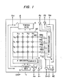
- a known semiconductor memory has a memory array AR of memory cells MC formed on a chip 1.
- An X decoder (including a driver) 3 selects memory cells MC in a row direction
- a Y decoder (including a driver) 4 selects memory cells MC in a column direction.
- the timing generator circuits 5 and 6 produce various internal timing pulses in synchronism with a clock pulse so as to control various circuit operations.
- Supply voltages Vcc for example, 5 volts
- V SS (0 volt) are fed to the circuits.
- a wiring material of low resistivity such as aluminium is used for power source lines for the supply voltages V CC and V SS or timing signal lines for various internal timings. Aluminium of the same layer.is used within the memory array AR.
- a reading operation is performed as stated below.
- the X decoder 3 is started.
- a word line X 0 for example, is consequently selected from among a plurality of word lines X 0 - X 3
- a select pulse is delivered to the word line X 0
- the memory cells MC connected therewith deliver read signals to corresponding data lines Y 0 - Y 3 .
- a select signal from the Y decoder 4 applied through a Y control line 8 turns on a switch SW 0 to select the data line Y 0
- the signal read out to the data line Y 0 is delivered to an input/ output line I/O through the switch SW 0 and is externally provided as a data output D 0
- a data input D i is sent to the input/output line I/O, the switch SW 0 and the data line Y 0 by a write enable signal WE, and the data is written into the memory cell MC which is connected at the intersection point between the data line Y 0 and the selected word line X 0 .
- the power source lines of the supply voltages V CC , V SS as well as the lines of the various timing signals and the memory array employ the identical conductor layer, so that they must be formed in regions separate from each other, making it impossible to reduce the area of the chip.
- the semiconductor memory is encased in a dual in-line package, the shorter side of the chip needs to be made small.
- the construction of the prior art devices has limited any reduction in this dimension.
- wiring leads such as power source lines and various timing signal lines extend in a direction intersecting the data lines of the memory array, and these wiring leads are formed within the memory array by the use of a conductor layer different from that forming the word lines and the data-.lines.
- the wiring leads extend in a direction intersecting the data lines, there is little capacitive coupling of the wiring per data line, and the data lines are not significantly affected by the signals of the wiring leads.
- capacitive coupling increases and greatly affects the data lines having small signals, so that there is a risk of malfunction of the semiconductor memory.
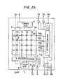
- Fig. 2A shows one embodiment of the present invention, in which the same parts as in Fig. 1 are assigned the same symbols.
- Fig. 2B is a sectional view taken along line A - A' in Fig. 2A.
- wiring leads P such as power source lines and various timing signal lines, are arranged so as to intersect the data lines Y 0 - Y 3 within the memory array AR.
- the word lines X 0 - X 3 are formed of a self-alignment material such as polycrystalline silicon or silicide
- the data lines Y - Y 3 are formed of a first layer of aluminum
- the power source lines and various timing signal lines P are formed of a second.layer of aluminum.
- the wiring lead P, the data line Y 0 and the word line X 0 are insulated therebetween by insulator films (Si0 2 ). They are formed on a P-type silicon substrate.
- the power source line and various timing signal lines P pass within the memory array AR, and hence, the shorter side of the chip can be shortened to that extent. Moreover, since the various timing signal lines intersect the data lines Y 0 - Y 3 , coupled capacitances are smaller than in the case of arraying them in parallel, and the small read signals of the data lines are less affected.
- the power source line and various timing signal lines P are arranged on the memory array AR, only some of them need be arranged on the memory array. In this case, the shorter side of the chip can be reduced to the extent of the occupying area of the lines arranged on the memory array.
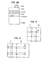
- Fig. 3 shows another embodiment of the present invention.
- the influence of the capacitive coupling on the small signals of the data lines is little, but the capacitive coupling of the wiring leads with the word lines arises.
- This second embodiment is appropriate when this capacitive coupling becomes a problem.
- Fig. 3 only the word lines X 0 , X 1 and the data lines Y 0 , Y 1 are illustrated.
- the power source line and the various timing signal lines are coupled to the plurality of word lines X 0 , X 1 .
- the power source line and various timing signal lines P intersect one word line and are passed near the other word line. This is the point of difference from the circuit of Fig. 2.
- this measure eliminates the drawback that, since the power source line and various timing signal lines are close to a specified word line (for example, the word line X 0 ), only this word line has an increased capacitance as compared with another word line (for example, the word line X 1 ) and is hampered from cperating at high speed.
- the power source line is thick and extends over a plurality of word lines, it may intersect the plurality of word lines.
- Fig. 4 shows another embodiment of the present invention, having improvements in the circuit of Fig. 2A.
- This third embodiment is the application of the present invention to a folded bit line arrangement cell.
- the detailed structure of the folded bit line arrangement cell is described in, e. g., IEEE PROC., Vol. 130, Pt. I. No. 3, p. 127, June 1983.
- Data lines are constructed of pair lines D and D t and a memory cell MC which is composed of a transistor and a capacitor is connected to one of the two intersection points between the pair lines and a word line X.
- the points of difference from Fig. 2A are that the signals of the two data lines are differentially amplified by a sense amplifier SA, and that these two data lines intersect the same timing signal line P.
- a half precharge system may be adopted. This system is such that, before stored information is read out from a memory cell, data lines are precharged to the intermediate level of two voltages "1" and "0" to be written into the memory cell. It is described in, for example, the official gazette of Japanese Patent Application Laying-open No. 54-63632 or ISSCC 1984 Digest of Technical Paper, p. 276, "A 288kb CMOS Pseudo SRAM” and p. 278, "A Sub 100ns 256k DRAM in CMOS III Technology".
- the folded bit line arrangement cell has been exemplified.
- the wiring lead P such as the timing signal line is laid so as to intersect the paired lines respectively.
- noise components attributed to the capacitive coupling between the wiring lead P and the data lines are cancelled. This holds true of a flip-flop type static memory.
- the flip-flop type static memory has signal lines in a relationship complementary to each other for one memory cell. Since the complementary signal lines are laid in common for a plurality of memory cells, they are arranged in parallel with each other. Accordingly, the wiring lead P such as the timing signal line can be laid so as to intersect the complementary signal lines respectively, as in the case of the folded bit line arrangement cell, and the noise components ascribable to the capacitive coupling between the wiring lead P and the data lines are cancelled.
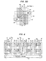
- Fig. 5A shows an example in which a large number of sub arrays 12a - 12d are driven by a single Y decoder.
- Each of the sub arrays is constructed of folded bit line arrangement cells.
- One of the word lines X 0 - X 7 of the respective sub arrays is selected by an X decoder 3 (including a driver).
- Each of the sub arrays 12a - 12d is provided with one pair of input/ output lines I/O.
- the signal of the memory cell MC connected to the word line X 0 selected by the X decoder 3 appears on a sub data line D 00 .
- a switch SW is driven by means of a Y control line YC 0 selected by the Y decoder 4, and the amplified signals are read out on one pair of input/output lines I/0(0).
- the other sub arrays 12b - 12d have similar arrangements.
- the switches SW of the respective sub arrays are driven by common Y control lines YC 0 and YC l .
- the signals of one sub data line pair are read out from each of the sub arrays 12a - 12d to the corresponding one of the input/output lines I/O(O) - 1/0(3).
- the wiring leads P which consists of the power source line for feeding a supply voltage V and the signal lines of various timings (in the figure, only ⁇ is illustrated), are formed by the sane conductor layer as that of the Y control lines YC 0 , YC 1 . Accordingly, in order to prevent the wiring leads P and the Y control lines from overlapping, the switches are disposed on the side of the sub array 12d near to the Y decoder 4, whereby the Y control lines parallel to the sub data lines are prevented from extending deep into the sub array 12d. Thus, the wiring leads P which orthogonally intersect the sub data lines can be arranged within the sub array 12d.
- Fig. 5B is a layout pattern of the part E of Fig. 5A enclosed with a dotted line.
- Fig. 5C is a sectional view taken along line B - B' in Fig. 5B.
- the storage capacitance C of the memory cell which is a hatched part in Fig. 5B, is formed between a first layer of polycrystalline silicon (POLY1 in Fig. 5C) and a p-type substrate pSUB with a thin oxide film Si0 2 held therebetween.
- the data line D' is formed of a first layer of aluminum which is connected with a diffused layer n + through a contact hole (CH in the figures).
- Symbol INS in Fig. 5C denotes an inter-layer insulator film which is located between the data line D' and the Y control line YC.
- the word lines X are formed of a second layer of polycrystalline silicon (POLY2).
- broken lines in Fig. 5B indicate the data lines. Indicated by a two-dot chain line is the Y control line, which is formed of a second layer of aluminum that lies over the first layer of aluminum.
- the wiring leads P are formed of the second layer of aluminum likewise to the Y control lines.
- Fig. 5D is a diagram of another layout of the part E of Fig. 5A enclosed with the dotted line.
- the difference from Fig. 5B is that the sub data lines D, D' and the Y control line YC are formed of the same conductor layer or the first layer of aluminum. In the figure, therefore, the sub data lines D, D' and the Y control line YC are indicated by the same dotted lines. Since the sub data lines and the Y control lines are arranged in parallel and do not overlap each other, they can be formed of the same conductor layer.
- the wiring leads P are formed of the second layer of aluminum, and the word lines are formed of self-alignment material such as polycrystalline silicon.
- the wiring leads P orthogonally intersecting the sub data lines and the Y control lines extending in parallel therewith are not of the same conductor layer, the wiring leads P can be arranged using the entire region on the sub array.
- the X decoder is recommended to be laid out by the use of the first layer of alucinum. This measure facilitates the layout because it is free from the trouble of changing the connection of the power source line and various tiding signal lines to another conductor layer in the X decoder portion and then passing the lines within the X decoder.
- Fig. 6 shows an embodiment which has improved the circuit arrangement of Fig. 5A.
- the same parts as in Fig. 5A are assigned the same symbols.
- the point of difference from the circuit arrangement in Fig. 5A is that the Y decoder 4 is arranged between the sub arrays, and that the Y control lines YC 0 , YC 1 are extended bidirectionally so as to drive the sub arrays on both sides of the Y decoder. In order to balance the Y control lines, the numbers of the sub arrays on both the sides are equalized.
- the fifth embodiment not only the sub array 12d, but also the sub array 12a is provided with a space in which the power source line V CC and various timing signal lines P' are arranged without passing the Y control lines YC 0 , YC 1 .
- the fifth embodiment can furnish the power source and timing signal lines with an area double that of the circuit arrangement in Fig. 5A.
- Fig. 7 shows an embodiment which has improved the sub arrays of the circuit arrangements in Fig. 5A and Fig. 6.
- Data lines D 0 , D 0 are connected to nodes CD 0 , CD 0 through a switching circuit GC.
- Data lines D 0 ', D 0 ' are also connected to the nodes CD 0 , CD 0 through a switching circuit GC.
- a sense amplifier SA, an active restore circuit AC, a precharge circuit PC and a switching circuit SW are connected to the nodes CD 0 , CD 0 .
- four sets of circuits PD (PD 0 , PD 1 , PD 2 and PD 3 ) in each of which they are combined are shown.
- the precharge circuit PC precharges all the nodes (D 0 , Dot CD 0 , CD 0 , D 0 ', D 0 ', etc.) to V CC . This is called "half precharge".
- a word line X 0 is selected by an X decoder (not shown) to provide a word pulse ⁇ xo , a memory cell MC connected thereto is selected.
- a minute signal voltage which is determined by the storage capacitance C s of the memory cell MC and the capacitance of the data line D 0 is delivered to this data line.
- a reference voltage is delivered from a dummy cell DC to the data line D 0 by turning on a pulse O DX2 .
- the dummy cell DC is not particularly needed in the half precharge system, but the use thereof is more effective when it is desired to cancel noise components.
- the switching circuit GC connected to the data lines (D 0 ', D 0 ') on the side to which the memory cell MC to be selected belongs is turned off by a control signal GC.
- the switch GC remains turned on. Accordingly, signals corresponding to the information from the memory cell MC appear at the nodes D O , CD O , while the reference voltage from the dummy cell DC appears at the nodes Do t CD O .
- the reference voltage is set at substantially an intermediate potential between read voltages which appear at the node CD O in correspondence with the information "1" and "0" of the memory cell MC.
- the sense amplifier SA is operated by a start pulse ⁇ SA so as to amplify the differential voltage. Since the sense amplifier SA is formed of n-channel MOSFETs, it cannot charge the node CD O or CD O though it can discharge the same. Therefore, the active restore circuit AC is operated by a start pulse ⁇ AC so as to perform the charging. To this end, the active restore circuit AC isformed of p-channel MOSFETs.
- a control signal is delivered to the Y control line YC 0 selected by a Y decoder (not shown), and the amplified voltage is differentially delivered to paired common input/output lines I/0(0) via the switch SW.
- Input/output lines I/0(0), 1/0(1) are formed of the same conductor layer as that of the power source line or various timing signal lines.
- the merits of the present circuit arrangement are as follows. Since the common input/output lines are laid near the sense amplifier SA, data can be read and written at high speed. In addition, since the precharge circuit, sense amplifier and active restore circuit are common to the two data line pairs, the area decreases to that extent.
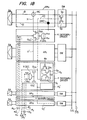
- Fig. 9 shows an example in which the word lines are divided into sub word lines as to the two sub arrays 12a and 12b of the circuit arrangement in Fig. 5A.
- the sub array 12a in Fig. 5A is divided into arrays APASO and APAS2 in the lengthwise direction of the word lines, and the other-sub array 12b into arrays APAS1 and APAS3.
- X decoders 3a and 3b are disposed between the respective divided arrays.
- the memory has a folded bit line arrangement cells as shown in Fig. 7.
- the single sense amplifier SA, precharge circuit PR, active restore circuit AC and switch SW are shared by the two pairs of data lines, whereas in the embodiment of Fig. 9, a single sense amplifier etc. are employed for one pair of data lines. Accordingly, the present embodiment differs from the circuit arrangement of Fig. 7 in that the switching circuits GC, GC are not present, but it is the same in regard to the other circuits.
- Timing signal lines P 1 , P 2 between timing generator circuits 5 and 6 for generating various timing signals are formed of the second layer of aluminum similarly to Y control lines YC 0 - YC 3 extended from a Y decoder 4.
- the switches SW are disposed on one side of the arrays nearer to the Y decoder 4. Accordingly, the Y control lines YC O -YC 3 from the Y decoder 4 extend to intermediate positions of the outer arrays APASO, APAS2 as viewed from the Y decoder 4 and are connected to the switches SW.
- the timing signal lines between the timing generator circuits can therefore be arranged in the remaining regions of the arrays APASO, APAS2.
- the timing signal lines P 1 , P 2 are arranged so as to couple with a plurality of sub word lines to avoid the influence of a malfunction ascribable to the capacitive coupling with the sub word line, as illustrated in Fig. 3.
- the timing signal line P is bent within the array so as to be also coupled with another word line, while the timing signal line P 2 is bent between the arrays so as to be also coupled with another sub word line.
- the Y control lines YC 0 - YC 3 and the data lines may be made of the first layer of aluminum, and the timing signal lines P 1 , P 2 the second layer of aluminum.
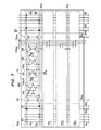
- Fig. 10 shows an example in which the Y decoder is disposed in parallel with the X decoder in order to more reduce the shorter side of the chip.
- Y decoder 4 is juxtaposed to the X decpder 3.
- the power source lines and timing signal lines are laid in the direction orthogonally intersecting the data lines.
- the Y decoder Since, in the present embodiment, the Y decoder is in parallel with the X decoder, the Y control lines which control the switches for connecting the data lines and the input/output lines must be arranged on the memory array so as to avoid increase in the occupying area attributed to the prolongation of the Y control lines.
- the power source lines and tiding signal lines are formed of the same layer as that of the Y control lines 8; and they are arranged on that part of the memory array which is other than the region for the Y control lines 8.
- the memory array AR in the prior art is formed of a diffused layer, polycrystalline silicon or aluminum
- two layers of aluminum may be formed so as to lay the Y control lines YC 0 - YC 3 by the use of the second layer of aluminum.
- the power source lines and various internal timing signal lines can be passed within the memory array 2 by, for example, changing them from the wiring leads of the first layer of aluminium to those of the second layer of aluminium via through holes midway (points CT in the figure).
- the length of one side of the chip may be shortened in correspondence with the change in size of the Y decoder 4, the power source lines etc.
- a corresponding increase in the length of the other side of the chip but this is not a serious problem in practical use.
- the reason is that in a dual in-line package, the length of the longer side of the chip is relatively surplus, as is apparent from the shape of the chip.
- the pitch of the word lines X 0 - X 3 and that of the Y control lines YC 0 - YC 3 need not always be the same.
- the pitch of the Y control lines YC 0 - YC 3 is made smaller, the power source lines and internal timing signal lines may be passed within the array in a larger number to that extent. Therefore, the number of wiring leads which are inevitably laid outside the array decreases, and in effect, the length of the shorter side of the chip can be rendered still smaller.
- the Y control lines 8 and the power source lines are formed of the same conductor layer. It is also possible, however, to form the Y control lines by the use of the second layer of aluminum and the power source lines by the use of a third layer of aluminum.
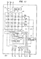
- Fig. 11 shows a modified embodiment of the circuit arrangement in Fig. 10.
- the switches SW O , SW 1 are simultaneously controlled to connect two input/output lines i/o, i/o' with the respectively corresponding data lines Y 0 , Y 1 .
- One of the two input/output lines i/o, i/o' is selected by a data selector circuit 10, and is connected to the input/output line I/ ⁇ .
- the exchange signals of the input/output lines i/o, i/o' are controlled by the data selector circuit 10.
- the merit of the present system is that the semiconductor memory is easy to manufacture because the pitch of the control lines 8 can be rendered large. In a case where the number of bits in the memory array is still larger, four or eight switches can also be controlled at once by the single Y control line 8.
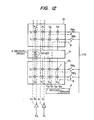
- Fig. 12 shows another modification of the circuit arrangement in Fig. 10. In this modification, the same portions are assigned the same symbols.
- the memory array is divided into portions 2a and 2b, between which the X decoder 3 is disposed.
- the word lines are divided into sub word lines (X 0 - X 3 , X 0 ' - X 3 '), and the length per word line is shortened.
- This arrangement can reduce the resistance components of the word lines and shorten the delay times thereof.
- the X decoder is between the memory arrays 2a and 2b, address signal lines a 0 , a 0 , a and a 1 to be connected to the X decoder are arranged on the memory array.
- the address signal lines are formed of a conductor layer different from that of the memory array in the prior art, they can be arranged on the memory array.
- an arrangement is also possible in which a plurality of sets each consisting of the memory array 2a, the X decoder 3 and the memory array 2b are repeated in the vertical direction and in which the Y decoder 4 and the address signal lines a 0 - a l can be used in common for the repeated sets.
- the chip area can be reduced in correspondence with the parts omitted owing to the common use.
- the Y decoder 4 can be placed between the memory arrays 2a and 2b in adjacency to the X decoder 3.
- the power source lines etc. can be rendered common to the X decoder 3 and the Y decoder 4 owing to the close positions thereof, so that the chip area can be furthermore reduced.
- FIG. 12 shows an example in which the data lines are divided into portions Y 0 - Y 0 ', Y 3 - Y 3 '.
- the memory array is divided into sub arrays 12a, 12b.
- the same address signal lines a 0 , a O are connected to X decoders 3a, 3b disposed in correspondence with the respective sub arrays, and each of the X decoders selects either of two word lines.
- the Y decoder 4 delivers a select signal to only one of four Y control lines.
- Switches SW 0 - SW 3 which control the connections between the data lines (Y 0 - Y 3 ) of the sub array 12a and the input/output line i/o respectively, and switches SW 0 ' - SW 3 ', which control the connections between the data lines (Y 0 ' - Y 3 ') of the sub array 12b and the input/output line i/o' respectively, are respectively operated by the signals of the common Y control lines 8.
- Read signal voltages are simultaneously delivered to the input/output lines i/o and i/o', and one of them is selected by the data selector circuit 10 and is delivered to the input/output line I/0.
- the present embodiment has the advantage of easy manufacture because the pitch of the Y control lines 8 can be rendered great.
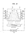
- Fig. 14 shows an example in which the two sets of switches SW 0 - SW 3 and SW 0 ' - SW 3 ' are arranged separate from each other.
- the Y decoder 4 has two sets of Y control lines YC 0 - YC 3 and YC 0 ' - YC 3 ', which are respectively connected to the switches SW 0 - S W 3 and SW 0 ' -SW 3 ⁇ of the sub arrays 12a and 12b.
- the Y decoder selects one of the respectively two corresponding Y control lines.
- the Y decoder when the Y decoder is constructed so as to be capable of selecting only any one of the eight control lines YC 0 - YC 3 and YC 0 ' - YC 3 ', only either of the input/output lines i/o and i/o' can be supplied with a read signal.
- the .other input/output line as mentioned above can be diverted to the input/output line i/o or i/o' of another sub array.
- the two read signals simultaneously delivered to the input/output lines i/o and i/o' need not be always selected into the single signal by the use of the data selector circuit 10.
- the read signals may be directly delivered without passing them through the data selector circuit 10.
- Fig. 15 shows an example in which one read signal output for the input/output line 1/0 is provided at all times.
- the present embodiment can reduce the chip area to the extent that the input/output lines i/o, i/o' have changed into one.
- the switches SWOt SW 0 ' etc. are controlled by independent Y control lines YC 0 , YC 4 etc. as in Fig. 14.
- two input/output lines I/0 belonging to the switch SW O and to the switch SW 0 ' can be prepared so as to derive read voltages to the two input/output lines I/O by simultaneously applying select pulses to the Y control lines, for example, YC 0 and YC 4 to simultaneously control the switches SW 0 and SW 0 '.
- each memory cell has the single data line (Y line), but it is obvious that the invention is also applicable to arrangements using pairs of data lines. shows
- Fig. 16 / a practicable embodiment for Fig. 12 which employs folded data line arrangement cells.
- Data lines are composed of pair lines D, D, and one memory cell MC (white circle in the figure) constructed of a transistor and a capacitor connected to one of the two intersection points between the pair lines and a word line.
- MC white circle in the figure
- a select pulse has been impressed on the word line X o by an X driver 3 whereby a minute signal voltage corresponding to information "1" or "0" has been derived from the memory cell to the data line D
- a dummy word line DX 0 is simultaneously selected by the X decoder 3, and a predetermined reference voltage is delivered from the dummy cell DMC (black circle in the figure) to the data line D.
- the reference voltage is set at the middle point of the signal voltages of the information "1" and "0"
- the read signal voltage is amplified by a sense amplifier SA to discriminate "1" or "0".
- the word line is formed of a material of comparatively high resistivity such as polycrystalline silicon or silicide, so that the memory device is divided in four in the direction of the word lines after the arrangement of Fig. 12.
- control lines (YC 0 - YC 3 ) are made of wiring leads of a second layer of aluminum.
- they may be wiring leads of the first layer of aluminum if the data lines of the folded data line arrangement cell are formed of a third layer of polycrystalline silicon by way of example. In this case, a problem in manufacture attendant especially upon the wiring leads of the second layer of aluminum is avoided, and there is the advantage of cost curtailment.
- the data pair lines and the Y control lines YC may well be made of the same material, for example, the first layer of aluminum.
- a Y decoder including a driver
- the number of the Y control lines increases in the direction of the shorter side of the chip, and the Y control lines protrude from the sub array 12a in some shapes of matrices. Therefore, the Y decoder is arranged between sub arrays 12c and 12e as shown in the figure, thereby to halve the number of the Y control lines con- tributive to the direction of the shorter side of the chip.
- the present example is an example of application of Fig.
- one Y control line for example, TC 0 is used for controlling switches SW 0 , SW 0 and sim- ultaneously switches SW 0 ', SW 0 ' that belong to another sub array 12b. It is also possible, however, to lay independent control lines on the sub arrays 12a, 12b different from each other as in the modification of Fig. 15 and to use them for independently controlling the switches SW 0 , SW 0 and the switches SW 0 ', SW 0 ' by way of example, thereby to derive amplified signal voltages to input/output lines I/0, 1/0 ,1/0', I/O' at the same time.
- TC 0 Y control line
- one Y control line for example, YC 0 can be used for controlling two sets of switches SW 0 , SW 0 , SW 1 , SW 1 as in Fig. 11.
- two pairs of input/output lines I/0 are required in this case.
- the switches are arranged on the side opposite to the sense amplifiers, it is also possible to arrange the switches in proximity to the sense amplifiers or to arrange the sense amplifiers in proximity to the switches. In general, however, arranging the sense amplifiers outside the arrays as shown in the figure makes it easier to lay out the sense amplifiers whose layout areas are prone to increase. The reason is that, since no circuit is disposed on one side, the space can be effectively used.
- the plurality of Y control lines 8 (assumed to be the three-dimensional wiring of the uppermost layer) may be wired in a shape enveloping the greaps of switches to be-controlled, as illustrated in the figure, in order to prevent them from crossing the arrays. Further, the Y control lines may be wired as illustrated in the figure in order to mitigate the complicacy of design relevant to wiring lead delays in such a way that the lengths of the Y control lines to pass on the sub array 12a and the lengths of the Y control lines to pass on the sub array 12b are equalized to the utmost.
- the switches of the sub arrays 12a, 12b and those of the sub arrays 12e, 12f may be controlled by the Y control lines extended from the Y decoder on the left side, while the switches of the sub arrays 12c, 12d and those of the sub arrays 12g, 12h by the Y control lines extended from the Y decoder on the right side.
- the switches SW 1 , SW 1 and SW 1 ', SW 1 ' belonging to the sub arrays 12a and 12b by way of example, only one DRV 0 of two drivers for driving the two divided Y control lines respectively may be turned on to impress a pulse on the Y control line YC 1 .
- the other driver DRV 1 must be turned off so as not to apply a pulse to the Y control line YC 1 '.
- the reason is that two sorts of read signal voltages are simultaneously delivered (multiple selection) from the sub arrays 12a and 12b to the input/output lines I/O, I/O, resulting in a malfunction.
- the lines of the address signals a 0 , a 0 determining the X decoder, the address signals a 2 , a 2 determining the Y decoder, etc. pass on the sub arrays as stated before.
- the switches are controlled by the Y control lines belonging to the sides of the sub arrays 12a, 12b, as by using the Y control line YC 0 to control the switches SW 0 , SW 0 ,SW 0 ', SW 0 ', the Y control line YC 2 to control the switches SW 1 , SW 1 , SW 1 ', SW 1 ', the Y control line YC 1 to control the switches SW 2 , SW 2 , SW 2 '.
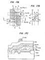
- Fig. 17A is a layout plan of the folded bit line arrangement cell
- Fig. 17B is a circuit diagram thereof
- Fig. 17C is a sectional view taken along line C - C' in Fig. 17A.
- a storage capacitance C s in the memory cell is formed between a first layer of polycrystalline silicon (POLY1 in the drawing) and a p-type substrate pSUB with a thin oxide film Si0 2 therebetween, and it is formed in a hatched part in Fig. 17A.
- a data line D 0 is formed of aluminum which is connected with a diffused layer n + by a contact hole (CHin the drawing).
- Symbol INS in Fig. 17C denotes an inter-layer insulator film which is located between a data line D 0 and a Y control line YC.
- Word lines X are formed of a second layer of polycrystalline silicon (POLY2).
- the word limes may be made cf silicide of lower resistivity or a material suited to self-alignment, such as molybdenum or tungsten.
- the data lines may well be formed of another layer different from the first layer of polycrystalline silicon (POLY1) or the second layer of polycrystalline silicon (POLY2). In this case, aluminum for the first layer of wiring can be used for the Y control lines YC as stated before.
- the embodiment in the drawing serves to reduce noise coupled to the data pair lines by the Y control line YC or noise coupled to the Y control line by the word line X. More specifically, the Y control line YC is arranged between the word lines X 0 and X 1 so as to reduce the coupled capacitances thereof.
- a wide wiring lead such as the power source line is laid on a plurality of word lines.
- Fig. 18 shows a part of the circuit arrangement of Fig. 16 in detail. In the drawing, only one pair of data lines are shown in each sub array.
- the sense amplifier SA in the figure is constructed of an ordinary flip-flop.
- small signal voltages read out from the memory cell MC and the dummy cell DMC to the data pair lines are amplified by the sense amplifier SA, and they are delivered as differential outputs to the input/output lines 1/0, I/O when transistors Q y , Q y are turned on by a pulse voltage applied to the selected y control line YC.
- a select signal is provided from an X decoder (X DEC) in accordance with address signals a Ox , ., a ix which run on arrays related with the selection of the word lines, whereupon word pulses are applied to a plurality of sub word lines (X, X') through drivers Q XD' Q' XD in accordance with a word line start signal ⁇ x .
- X DEC X decoder
- address signals a OY , ., a kY related with the selection of the Y control lines pass on the arrays, and a select signal is provided from a Y decoder (Y DEC) in accordance with them.
- a Y control line start pulse is applied and only the specified Y control line is supplied with the pulse and controls the switch SW.
- the pulse voltage which is applied to the Y control line is controlled so as to have an amplitude sufficiently higher than a supply voltage. dore specifically, assuming the supply voltage to be 5 V, when a pulse of 5 V is applied to
- a line ⁇ ' y' a pulse of 5 V is also delivered to the Y control line.
- a boosting clock signal ⁇ b having an amplitude of 5 V is applied from one end of a capacitor C b .
- the Y control line is eventually fed with a pulse ⁇ y which is such that a voltage with the pulse amplitude of the signal ⁇ b divided by the capacitance of the capacitor C b and the parasitic capacitance of the Y control line is added to the pulse ⁇ ' y .
- Such boosting technique has been applied to word lines in a conventional dynamic memory for the purpose of increasing charges to be stored in memory cells, and the similar technique is also usable for the Y control lines.
- symbols PD and PD' denote pull-down circuits for bringing non-selected Y control lines into low impedances.
- the pull-down circuit is provided in order to prevent the Y control line from developing noise due to the capacitive coupling with the word line, resulting in the malfunction of the switch SW.
- a high voltage is applied to the gate of a MOS transistor Q 1 by a precharge signal ⁇ p so as to turn on the MOS transistor Q 1 .
- all the Y control lines become low impedances which are goveraed by the impedances of the MOS transistors Q 1 , and the coupling noise is rendered unlikely to be induced as described before.
- the MOS transistors Q YD and Q 1 perform a ratio operation, with the result that a high voltage thereby determined is generated on the Y control line.
- a MOS transistor Q 2 is turned on, and the gate voltage of the MOS transistor Q 1 becomes 0 V to turn off this MOS transistor Q 1 . Since the ratio operation continues for a short time, the power consumption does not increase.
- a single control system may be farmed without preparing the two perfectly independent control systems which include the pulse lines ⁇ y , ⁇ y , drivers Q YD , Q' YD and Y control lines YC, YC'.
- the Y control lines YC and YC' cam be unified into a single control-line, so that one pull-down circuit suffices.
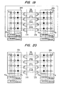
- Fig. 19 shows an example in which the present system is applied to the dynamic memory cell of an open data line arrangement cell.
- White circles in arrays indicate memory cells, and black circles dummy cells.
- the structure is detailed in the paper mentioned before.
- the present example is an example in which switches confront the inner sides of the arrays 22a, 22b. It differs from the arrangement of Fig. 13 in the following point.
- the memory cells belonging to the sub arrays 12a, 12b are independently selected, and the two independent data are applied to or from the input/output lines i/o, i/o', whereas in the embodiment of Fig. 19, one data is applied to or from the input/ output line I/O or I/O, and it is differentially applied.
- a Y control line is laid in parallel with the respective data lines D, D so as to have equal coupled capacitances with both the data lines D, D.
- the Y control lines are extended alternately from right and left Y decoders.
- the Y control line is lengthened in order tc equalize the coupled capacitances, it intersects another Y control line. Therefore, it is possible to equalize the length over which the Y control line and the data line D couple and the length over which the Y control line and the data line D couple. Accordingly, the electrical unbalance between the data lines D and D is liable to occur, resulting in great noise.
- FIG. 20 An embodiment in Fig. 20 is basically the same as the circuit arrangement of Fig. 19, and it differs only in that the Y control lines of the left Y decoder and those of the right Y decoder are arranged in the order of the data lines as reckoned from the uppermost one. Also in this case, likewise to the above, the data lines D, D become electrically unbalanced.
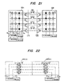
- Fig. 21 is basically the same as the circuit arrangement of Fig. 19, and it differs only in that all the switches are selected by the Y decoder disposed on the left side. Also in this case, the data lines D, D similarly become electrically unbalanced.
- the open data line arrangement cells are, in general, inferior in the signal-to- noise ratio, and in order to improve this drawback, the system of dividing the data lines as in Fig. 13 is common.
- the arrangement of Fig. 19 is simply multiplexed. That is, when the entirety of Fig. 19 is deemed a sub array AR(0), the arrangement of the sub array AR(0) is repeated in the direction of the data lines.
- the Y control lines are completed within the sub arrays AR, AR to which one set of sense amplifiers belong.
- Another method is such that, as shown in Fig. 22, Y control lines are laid and controlled in common between larger sub arrays AR(0), AR'(0). It is obvious that the data lines can be divided similarly on the basis of the concepts in Figs. 20 and 21.
- Fig. 23 shows an embodiment in the case where, as regards the open data line arrangement cells, switches SW are arranged at ends remote from sense amplifiers SA.
- the layout area of the sense amplifiers SA becomes large, so that when the switches are laid out in proximity thereto, the electrical balance between the data pair lines becomes difficult to be held. Therefore the present embodiment which separates the switches away from the sense amplifiers SA is important in practical use.
- the present embodiment is also considered a practical example of the arrangement of Fig. 14.
- the two data independent of each other are applied to or from the input/output lines i/o, i/o', whereas in the embodiment of Fig. 23, one data is differentially applied to or from the input/ output line I/0 or I/O .
- the advantage of the present embodiment is that the electrical balance of the respective data pair lines is substantially perfect.
- the reason is that the data lines D, D and Y control lines YC 3 , YC 3 ' are capacitively coupled substantially equally.
- two corresponding Y control lines such as the Y control lines 3 and YC 3 ', those YC 2 and YC 2 ', those YC 1 and YC 1 ' or those YC 0 and YC 0 ' are always selected by Y decoders, and the data of the memory cell selected by an X decoder is exchanged between the corresponding data pair line and the input/output line T/0 or I/0.
- Fig. 24 shows an expanded example of the arrangement of Fig. 23 corresponding to Fig. 22 in which the data lines are divided. Switches on the sides of input/ output lines I/0, I/O', which belong to sub arrays AR(0) and AR'(0), are controlled by the same Y control lines. Y control lines YC 3 , YC 3 ',YC 3 " are simultaneously selected, and data are exchanged with two pairs of input/output lines I/O, I/0, I/O', I/0'.
- the concrete wiring of the Y control lines for the open data line arrangement cells may be similar to that of Fig. 17.
- the semiconductor memory according to the present invention can be rendered slender, an elongate package preferably made of plastics can be used. As a result, the invention can reduce the packaging cost.
- one side of a chip can be shortened, and this is convenient for application to an elongate package.
- the invention do not only applies for a memory device having data lines for both inputing and outputing memory signals, but also applies for a memory device having two types of data lines, such that one type is for inputing memory signal and the other type is for outputing memory signal.
Landscapes
- Engineering & Computer Science (AREA)
- Microelectronics & Electronic Packaging (AREA)
- Computer Hardware Design (AREA)
- Semiconductor Memories (AREA)
- Dram (AREA)
- Static Random-Access Memory (AREA)
- Semiconductor Integrated Circuits (AREA)
- Read Only Memory (AREA)
Abstract
Description
- The present invention relates to a semiconductor memory.
- As illustrated in Fig. 1 of the accompanying drawings, a known semiconductor memory has a memory array AR of memory cells MC formed on a
chip 1. An X decoder (including a driver) 3 selects memory cells MC in a row direction,and a Y decoder (including a driver) 4 selects memory cells MC in a column direction. Also shown in Fig. 1 aretiming generator circuits timing generator circuits - In such prior-art semiconductor memory, a reading operation is performed as stated below. When external address signals A0 - A3 are received as inputs, the
X decoder 3 is started. When a word line X0, for example, is consequently selected from among a plurality of word lines X0 - X3, a select pulse is delivered to the word line X0, and the memory cells MC connected therewith deliver read signals to corresponding data lines Y0 - Y3. Meanwhile, assuming that a select signal from theY decoder 4 applied through aY control line 8 turns on a switch SW0 to select the data line Y0, the signal read out to the data line Y0 is delivered to an input/ output line I/O through the switch SW0 and is externally provided as a data output D0. In a writing operation, a data input Di is sent to the input/output line I/O, the switch SW0 and the data line Y0 by a write enable signal WE, and the data is written into the memory cell MC which is connected at the intersection point between the data line Y0 and the selected word line X0. - In such semiconductor memory, however, the power source lines of the supply voltages VCC, VSS as well as the lines of the various timing signals and the memory array employ the identical conductor layer, so that they must be formed in regions separate from each other, making it impossible to reduce the area of the chip. For example, when the semiconductor memory is encased in a dual in-line package, the shorter side of the chip needs to be made small. However, the construction of the prior art devices has limited any reduction in this dimension.
- According to the present invention, wiring leads such as power source lines and various timing signal lines extend in a direction intersecting the data lines of the memory array, and these wiring leads are formed within the memory array by the use of a conductor layer different from that forming the word lines and the data-.lines. Thus, it is possible to reduce the region to be occupied by the wiring leads and the area of the chip occupied by the memory array may be reduced. Also, since the wiring leads extend in a direction intersecting the data lines, there is little capacitive coupling of the wiring per data line, and the data lines are not significantly affected by the signals of the wiring leads. In contrast, when the data lines and the wiring leads are arranged in parallel, capacitive coupling increases and greatly affects the data lines having small signals, so that there is a risk of malfunction of the semiconductor memory.
- Embodiments of the present invention will now be described, by way of example, with reference to the accompanying drawings, in which:
- Fig. 1 is a diagram of the arrangement of a prior-art semiconductor memory;
- Fig. 2A is a diagram of the arrangement of an embodiment of the present invention, while Fig. 2B is a sectional view taken along line A - A' in Fig. 2A;
- Figs. 3 - 6 are diagrams each showing the arrangement of another embodiment of the present invention;
- Fig. 7 is a diagram of the arrangement of a subarray for use in the embodiment of Fig. 5A or 6, while Fig. 8 is a time chart of the operation of the subarray in Fig. 7;
- Figs. 9 - 12 are diagrams each showing the arrangement of another embodiment of the present invention;
- Figs. 13 - 15 are diagrams each elucidating the way of connection in the case of arranging X and Y decoders in parallel;
- Fig. 16 is a diagram showing a semiconductor memory constructed by combining the various embodiments of the present invention;
- Fig. 17A is a layout plan of a folded bit line arrangement cell for use in the semiconductor memory of Fig. 16, Fig. 17B is a circuit diagram of the folded bit line arrangement cell, and Fig. 17C is a sectional view of the folded bit line arrangement cell;
- Fig. 18 is a diagram showing a part of the circuit arrangement of Fig. 16 in detail; and
- Figs. 19 - 24 are diagrams each showing an example in the case of arranging the X and Y decoders of open data line arrangement memory cells in parallel.
- Fig. 2A shows one embodiment of the present invention, in which the same parts as in Fig. 1 are assigned the same symbols. Fig. 2B is a sectional view taken along line A - A' in Fig. 2A.
- The point of difference from the prior art in Fig. 1 is that wiring leads P, such as power source lines and various timing signal lines, are arranged so as to intersect the data lines Y0 - Y3 within the memory array AR. In this first embodiment, the word lines X0 - X3 are formed of a self-alignment material such as polycrystalline silicon or silicide, the data lines Y - Y3 are formed of a first layer of aluminum, and the power source lines and various timing signal lines P are formed of a second.layer of aluminum. The wiring lead P, the data line Y0 and the word line X0 are insulated therebetween by insulator films (Si02). They are formed on a P-type silicon substrate.
- In Fig. 2B, in order to facilitate understanding, the data line is also depicted as if seen in section.
- According to the present embodiment, the power source line and various timing signal lines P pass within the memory array AR, and hence, the shorter side of the chip can be shortened to that extent. Moreover, since the various timing signal lines intersect the data lines Y0 - Y3, coupled capacitances are smaller than in the case of arraying them in parallel, and the small read signals of the data lines are less affected.
- Although, in the present embodiment, all of the power source line and various timing signal lines P are arranged on the memory array AR, only some of them need be arranged on the memory array. In this case, the shorter side of the chip can be reduced to the extent of the occupying area of the lines arranged on the memory array.
- Fig. 3 shows another embodiment of the present invention. In the example of Fig. 2A, the influence of the capacitive coupling on the small signals of the data lines is little, but the capacitive coupling of the wiring leads with the word lines arises. This second embodiment is appropriate when this capacitive coupling becomes a problem. In Fig. 3, only the word lines X0, X1 and the data lines Y0, Y1 are illustrated.
- Concretely, the power source line and the various timing signal lines are coupled to the plurality of word lines X0, X1. To this end, the power source line and various timing signal lines P intersect one word line and are passed near the other word line. This is the point of difference from the circuit of Fig. 2. Thus, it is possible to reduce voltages which couple from the power source line and various timing signal lines to the word lines (X0 - X1) and voltages which couple from one selected word line to the power source line and various timing signal lines conversely. Consequently, this measure eliminates the drawback that, since the power source line and various timing signal lines are close to a specified word line (for example, the word line X0), only this word line has an increased capacitance as compared with another word line (for example, the word line X1) and is hampered from cperating at high speed. In a case where the power source line is thick and extends over a plurality of word lines, it may intersect the plurality of word lines.
- Fig. 4 shows another embodiment of the present invention, having improvements in the circuit of Fig. 2A.
- This third embodiment is the application of the present invention to a folded bit line arrangement cell. The detailed structure of the folded bit line arrangement cell is described in, e. g., IEEE PROC., Vol. 130, Pt. I. No. 3, p. 127, June 1983.
- Data lines are constructed of pair lines D and Dt and a memory cell MC which is composed of a transistor and a capacitor is connected to one of the two intersection points between the pair lines and a word line X. The points of difference from Fig. 2A are that the signals of the two data lines are differentially amplified by a sense amplifier SA, and that these two data lines intersect the same timing signal line P.
- In the third embodiment, even when the various timing signal lines P couple to the two data lines capacitively, voltages generated by the capacitive coupling become inphase between the two data lines and are cancelled at the differential amplification. For this reason, the capacitive coupling of the various titijmins signal lines affects the reading of data very slightly.
- In order to reduce voltages which are generated contrariwise by the capacitive coupling of the data lines to the various timing signal lines, a half precharge system may be adopted. This system is such that, before stored information is read out from a memory cell, data lines are precharged to the intermediate level of two voltages "1" and "0" to be written into the memory cell. It is described in, for example, the official gazette of Japanese Patent Application Laying-open No. 54-63632 or ISSCC 1984 Digest of Technical Paper, p. 276, "A 288kb CMOS Pseudo SRAM" and p. 278, "A Sub 100ns 256k DRAM in CMOS III Technology".
- With this system, in differentially amplifying the signals by means of the sense amplifier, a change at the time at which the signal of one'of the paired data lines becomes a high potential is substantially equal to a change at the time at which the signal of the other data line becomes a low potential, so that potentials attributed-to the capacitive coupling of the two data lines are cancelled.
- In the third embodiment of Fig. 4, the folded bit line arrangement cell has been exemplified. However, insofar as two paired lines whose signals are to be differentially amplified are juxtaposed and the wiring lead P such as the timing signal line is laid so as to intersect the paired lines respectively, noise components attributed to the capacitive coupling between the wiring lead P and the data lines are cancelled. This holds true of a flip-flop type static memory.
- More specifically, the flip-flop type static memory has signal lines in a relationship complementary to each other for one memory cell. Since the complementary signal lines are laid in common for a plurality of memory cells, they are arranged in parallel with each other. Accordingly, the wiring lead P such as the timing signal line can be laid so as to intersect the complementary signal lines respectively, as in the case of the folded bit line arrangement cell, and the noise components ascribable to the capacitive coupling between the wiring lead P and the data lines are cancelled.
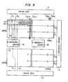
- Next, there will be elucidated an embodiment wherein the present invention is applied to a memory of the multi-divided data line system which is described in U. S. Patent Application No. 380409 (corresponding to Japanese Patent Application Laying-open No. 57-198592)
- Fig. 5A shows an example in which a large number of
sub arrays 12a - 12d are driven by a single Y decoder. - Each of the sub arrays is constructed of folded bit line arrangement cells. One of the word lines X0 - X7 of the respective sub arrays is selected by an X decoder 3 (including a driver). Each of the
sub arrays 12a - 12d is provided with one pair of input/ output lines I/O. When note is taken of thesub array 12a, the signal of the memory cell MC connected to the word line X0 selected by theX decoder 3 appears on a sub data line D00. After the signals of a sub data line pair D00,D 00 have been differentially amplified by a sense amplifier SA, a switch SW is driven by means of a Y control line YC0 selected by theY decoder 4, and the amplified signals are read out on one pair of input/output lines I/0(0). Theother sub arrays 12b - 12d have similar arrangements. The switches SW of the respective sub arrays are driven by common Y control lines YC0 and YCl. For example, where the Y control line YC0 has been selected, the signals of one sub data line pair are read out from each of thesub arrays 12a - 12d to the corresponding one of the input/output lines I/O(O) - 1/0(3). - In this fourth embodiment, the wiring leads P, which consists of the power source line for feeding a supply voltage V and the signal lines of various timings (in the figure, only φ is illustrated), are formed by the sane conductor layer as that of the Y control lines YC0, YC1. Accordingly, in order to prevent the wiring leads P and the Y control lines from overlapping, the switches are disposed on the side of the
sub array 12d near to theY decoder 4, whereby the Y control lines parallel to the sub data lines are prevented from extending deep into thesub array 12d. Thus, the wiring leads P which orthogonally intersect the sub data lines can be arranged within thesub array 12d. - Fig. 5B is a layout pattern of the part E of Fig. 5A enclosed with a dotted line. Fig. 5C is a sectional view taken along line B - B' in Fig. 5B.
- The storage capacitance C of the memory cell, which is a hatched part in Fig. 5B, is formed between a first layer of polycrystalline silicon (POLY1 in Fig. 5C) and a p-type substrate pSUB with a thin oxide film Si02 held therebetween. The data line D' is formed of a first layer of aluminum which is connected with a diffused layer n+ through a contact hole (CH in the figures). Symbol INS in Fig. 5C denotes an inter-layer insulator film which is located between the data line D' and the Y control line YC. The word lines X are formed of a second layer of polycrystalline silicon (POLY2). Further, broken lines in Fig. 5B indicate the data lines. Indicated by a two-dot chain line is the Y control line, which is formed of a second layer of aluminum that lies over the first layer of aluminum. The wiring leads P are formed of the second layer of aluminum likewise to the Y control lines.
- Fig. 5D is a diagram of another layout of the part E of Fig. 5A enclosed with the dotted line. The difference from Fig. 5B is that the sub data lines D, D' and the Y control line YC are formed of the same conductor layer or the first layer of aluminum. In the figure, therefore, the sub data lines D, D' and the Y control line YC are indicated by the same dotted lines. Since the sub data lines and the Y control lines are arranged in parallel and do not overlap each other, they can be formed of the same conductor layer. In this case, as in the layout of Fig. 5B, the wiring leads P are formed of the second layer of aluminum, and the word lines are formed of self-alignment material such as polycrystalline silicon.
- According to the layout of Fig. 5D, the wiring leads P orthogonally intersecting the sub data lines and the Y control lines extending in parallel therewith are not of the same conductor layer, the wiring leads P can be arranged using the entire region on the sub array.
- When the power source line and various timing signal lines are formed of the second layer of aluminum, the X decoder is recommended to be laid out by the use of the first layer of alucinum. This measure facilitates the layout because it is free from the trouble of changing the connection of the power source line and various tiding signal lines to another conductor layer in the X decoder portion and then passing the lines within the X decoder.
- Fig. 6 shows an embodiment which has improved the circuit arrangement of Fig. 5A. The same parts as in Fig. 5A are assigned the same symbols.
- The point of difference from the circuit arrangement in Fig. 5A is that the
Y decoder 4 is arranged between the sub arrays, and that the Y control lines YC0, YC1 are extended bidirectionally so as to drive the sub arrays on both sides of the Y decoder. In order to balance the Y control lines, the numbers of the sub arrays on both the sides are equalized. - In this fifth embodiment, not only the
sub array 12d, but also thesub array 12a is provided with a space in which the power source line VCC and various timing signal lines P' are arranged without passing the Y control lines YC0, YC1. In the case of forming the Y control lines and the wiring leads P by the use of the same conductor layer, therefore, the fifth embodiment can furnish the power source and timing signal lines with an area double that of the circuit arrangement in Fig. 5A. - Fig. 7 shows an embodiment which has improved the sub arrays of the circuit arrangements in Fig. 5A and Fig. 6.
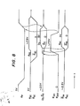
- Data lines D0,
D 0 CD 0 through a switching circuit GC. Data lines D0',D 0 ' are also connected to the nodes CD0,CD 0 CD 0 . In the figure, four sets of circuits PD (PD0, PD1, PD2 and PD3) in each of which they are combined are shown. - The embodiment will be described more in detail with reference to a time chart in Fig. 8. First, in accordance with a precharge signal φp, the precharge circuit PC precharges all the nodes (D0, Dot CD0, CD0, D0', D0', etc.) to

- Simultaneously, a reference voltage is delivered from a dummy cell DC to the data line
D 0 - Before the word line X0 is selected, the switching circuit
GC connected to the data lines (D0',D 0 ') on the side to which the memory cell MC to be selected belongs is turned off by a control signal GC. On the other hand, the switch GC remains turned on. Accordingly, signals corresponding to the information from the memory cell MC appear at the nodes DO, CDO, while the reference voltage from the dummy cell DC appears at the nodesDo tCD O . The reference voltage is set at substantially an intermediate potential between read voltages which appear at the node CDO in correspondence with the information "1" and "0" of the memory cell MC. Therefore, a minute differential voltage corresponding to the information "1" or "0" appears at the input end of the sense amplifier SA. Thereafter, the sense amplifier SA is operated by a start pulseφ SA CD O though it can discharge the same. Therefore, the active restore circuit AC is operated by a start pulse φAC so as to perform the charging. To this end, the active restore circuit AC isformed of p-channel MOSFETs. - Thereafter, a control signal is delivered to the Y control line YC0 selected by a Y decoder (not shown), and the amplified voltage is differentially delivered to paired common input/output lines I/0(0) via the switch SW. Input/output lines I/0(0), 1/0(1) are formed of the same conductor layer as that of the power source line or various timing signal lines.
- The merits of the present circuit arrangement are as follows. Since the common input/output lines are laid near the sense amplifier SA, data can be read and written at high speed. In addition, since the precharge circuit, sense amplifier and active restore circuit are common to the two data line pairs, the area decreases to that extent.
- Fig. 9 shows an example in which the word lines are divided into sub word lines as to the two
sub arrays - The
sub array 12a in Fig. 5A is divided into arrays APASO and APAS2 in the lengthwise direction of the word lines, and the other-sub array 12b into arrays APAS1 and APAS3.X decoders - The memory has a folded bit line arrangement cells as shown in Fig. 7. However, in the circuit trrangement of Fig. 7, the single sense amplifier SA, precharge circuit PR, active restore circuit AC and switch SW are shared by the two pairs of data lines, whereas in the embodiment of Fig. 9, a single sense amplifier etc. are employed for one pair of data lines. Accordingly, the present embodiment differs from the circuit arrangement of Fig. 7 in that the switching circuits GC, GC are not present, but it is the same in regard to the other circuits.
- Timing signal lines P1, P2 between
timing generator circuits Y decoder 4. - Since, in the present embodiment, folded bit line arrangement cells are employed, the switches SW are disposed on one side of the arrays nearer to the
Y decoder 4. Accordingly, the Y control lines YCO -YC3 from theY decoder 4 extend to intermediate positions of the outer arrays APASO, APAS2 as viewed from theY decoder 4 and are connected to the switches SW. The timing signal lines between the timing generator circuits can therefore be arranged in the remaining regions of the arrays APASO, APAS2. - The timing signal lines P1, P2 are arranged so as to couple with a plurality of sub word lines to
avoid the influence of a malfunction ascribable to the capacitive coupling with the sub word line, as illustrated in Fig. 3. By way of example, the timing signal line P is bent within the array so as to be also coupled with another word line, while the timing signal line P2 is bent between the arrays so as to be also coupled with another sub word line. - In the arrangement of Fig. 9, only some of the four arrays APASO - APAS3 are sometimes operated at the same time without operating all of them. This includes the following two cases:
- (1) By driving the
X decoder 3a and theY decoder 4, the arrays in the direction of the sub word lines, such as the arrays APASO and APAS2, are operated.
In this case, the voltage fluctuations of the data lines existing directly below the timing signal lines P1, P2 take place over the full lengths of the timing signal lines, so that great noise voltages are induced on the timing signal lines P1, P2 through the coupled capacitancesbetween the timing signal lines and the data lines. - (2) The upper or lower sub word lines of the
X decoders - In this case, the voltage fluctuations of the data lines existing directly below the timing signal lines F1, P2 take place in only a half of the region in the above case, so that noise voltages decrease to half.
- When driving some of the arrays, accordingly, it is preferable to operate the sub arrays in the direction of the data lines. In the arrangement of Fig. 9, the Y control lines YC0 - YC3 and the data lines may be made of the first layer of aluminum, and the timing signal lines P1, P2 the second layer of aluminum.
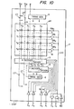
- Next, Fig. 10 shows an example in which the Y decoder is disposed in parallel with the X decoder in order to more reduce the shorter side of the chip.
- Different from the arrangement of Fig. 2A is that the
Y decoder 4 is juxtaposed to theX decpder 3. - The power source lines and timing signal lines are laid in the direction orthogonally intersecting the data lines.
- Since, in the present embodiment, the Y decoder is in parallel with the X decoder, the Y control lines which control the switches for connecting the data lines and the input/output lines must be arranged on the memory array so as to avoid increase in the occupying area attributed to the prolongation of the Y control lines. To this end, the power source lines and tiding signal lines are formed of the same layer as that of the
Y control lines 8; and they are arranged on that part of the memory array which is other than the region for the Y control lines 8. - For example, when the memory array AR in the prior art is formed of a diffused layer, polycrystalline silicon or aluminum, two layers of aluminum may be formed so as to lay the Y control lines YC0 - YC3 by the use of the second layer of aluminum. The power source lines and various internal timing signal lines can be passed within the
memory array 2 by, for example, changing them from the wiring leads of the first layer of aluminium to those of the second layer of aluminium via through holes midway (points CT in the figure). - Thus, the length of one side of the chip may be shortened in correspondence with the change in size of the
Y decoder 4, the power source lines etc. There is, however, a corresponding increase in the length of the other side of the chip, but this is not a serious problem in practical use. The reason is that in a dual in-line package, the length of the longer side of the chip is relatively surplus, as is apparent from the shape of the chip. The pitch of the word lines X0 - X3 and that of the Y control lines YC0 - YC3 need not always be the same. For example, if the pitch of the Y control lines YC0 - YC3 is made smaller, the power source lines and internal timing signal lines may be passed within the array in a larger number to that extent. Therefore, the number of wiring leads which are inevitably laid outside the array decreases, and in effect, the length of the shorter side of the chip can be rendered still smaller. - If the embodiment of Fig. 10, the
Y control lines 8 and the power source lines are formed of the same conductor layer. It is also possible, however, to form the Y control lines by the use of the second layer of aluminum and the power source lines by the use of a third layer of aluminum. - Fig. 11 shows a modified embodiment of the circuit arrangement in Fig. 10. Using a single Y control line, e. g., YCO, the switches SWO, SW1 are simultaneously controlled to connect two input/output lines i/o, i/o' with the respectively corresponding data lines Y0, Y1. One of the two input/output lines i/o, i/o' is selected by a
data selector circuit 10, and is connected to the input/output line I/θ. - Thus, the exchange signals of the input/output lines i/o, i/o' are controlled by the
data selector circuit 10. The merit of the present system is that the semiconductor memory is easy to manufacture because the pitch of thecontrol lines 8 can be rendered large. In a case where the number of bits in the memory array is still larger, four or eight switches can also be controlled at once by the singleY control line 8. - Fig. 12 shows another modification of the circuit arrangement in Fig. 10. In this modification, the same portions are assigned the same symbols.
- The point of difference from the circuit arrangement in Fig. 10 is as stated below. In order to eliminate the delay of word lines attributed to the resistance components thereof in a case where the word lines are formed of a resistive material, for example, polycrystalline silicon or silicide, the memory array is divided into
portions 2a and 2b, between which theX decoder 3 is disposed. Thus, the word lines are divided into sub word lines (X0 - X3, X0' - X3'), and the length per word line is shortened. - This arrangement can reduce the resistance components of the word lines and shorten the delay times thereof.
- Since, in the present embodiment, the X decoder is between the
memory arrays 2a and 2b, address signal lines a0,a 0 , a anda 1 X decoder 3 and thememory array 2b are repeated in the vertical direction and in which theY decoder 4 and the address signal lines a0 -a l Y decoder 4 can be placed between thememory arrays 2a and 2b in adjacency to theX decoder 3. Thus, the power source lines etc. can be rendered common to theX decoder 3 and theY decoder 4 owing to the close positions thereof, so that the chip area can be furthermore reduced. - Whereas the arrangement of Fig. 12 has divided the word lines, an arrangement in Fig. 13 shows an example in which the data lines are divided into portions Y0 - Y0', Y3 - Y3'. The memory array is divided into
sub arrays - In the present embodiment, the same address signal lines a0,
a O X decoders Y decoder 4 delivers a select signal to only one of four Y control lines. Switches SW0 - SW3, which control the connections between the data lines (Y0 - Y3) of thesub array 12a and the input/output line i/o respectively, and switches SW0' - SW3', which control the connections between the data lines (Y0' - Y3') of thesub array 12b and the input/output line i/o' respectively, are respectively operated by the signals of the common Y control lines 8. - Read signal voltages are simultaneously delivered to the input/output lines i/o and i/o', and one of them is selected by the
data selector circuit 10 and is delivered to the input/output line I/0. The present embodiment has the advantage of easy manufacture because the pitch of theY control lines 8 can be rendered great. - Fig. 14 shows an example in which the two sets of switches SW0 - SW3 and SW0' - SW3' are arranged separate from each other. In the present embodiment, the
Y decoder 4 has two sets of Y control lines YC0 - YC3 and YC0' - YC3', which are respectively connected to the switches SW0 - SW 3 and SW0' -SW3` of thesub arrays - When it is intended to simultaneously control, for example, the switches SW0 and SW0' by means of the single
Y control line 8 as illustrated in Fig. 13, there arises the inconvenience that the wiring leads of the second layer of aluminum indicated by dotted lines in the figure intersect the other Y control lines. Therefore, the switches SW0 and SW0' must be individually controlled by the independent Y control lines (YC3, YC3') within the specified sub arrays as in the circuit arrangement shown in Fig. 14. As a modification, when the Y decoder is constructed so as to be capable of selecting only any one of the eight control lines YC0 - YC3 and YC0' - YC3', only either of the input/output lines i/o and i/o' can be supplied with a read signal. This brings forth the advantage that the other input/output line supplied with no output can be used as a signal line having another function. For example, in an arrangement wherein the Y control line is divided into a larger number of parts and wherein thesub arrays - In Fig. 13 or 14, the two read signals simultaneously delivered to the input/output lines i/o and i/o' need not be always selected into the single signal by the use of the
data selector circuit 10. In some memories, it is desired to simultaneously deliver a large number of read signals out of the chip and to increase the quantity of utilizable data. In this case, the read signals may be directly delivered without passing them through thedata selector circuit 10. - Fig. 15 shows an example in which one read signal output for the input/
output line 1/0 is provided at all times. As compared with the arrangement of Fig. 13 or 14, the present embodiment can reduce the chip area to the extent that the input/output lines i/o, i/o' have changed into one. The switches SWOt SW0' etc. are controlled by independent Y control lines YC0, YC4 etc. as in Fig. 14. However, in some cases, for example,
where a large number of data are to be read out in parallel, two input/output lines I/0 belonging to the switch SWO and to the switch SW0' can be prepared so as to derive read voltages to the two input/output lines I/O by simultaneously applying select pulses to the Y control lines, for example, YC0 and YC4 to simultaneously control the switches SW0 and SW0'. - The above examples of arrangements are applicable to all semiconductor memory cells such as the memory cells of a dynamic MOS memory, a flip-flop type static memory and a ROM. It has been presumed in the examples that each memory cell has the single data line (Y line), but it is obvious that the invention is also applicable to arrangements using pairs of data lines. shows
- Fig. 16 / a practicable embodiment for Fig. 12 which employs folded data line arrangement cells. Data lines are composed of pair lines D, D, and one memory cell MC (white circle in the figure) constructed of a transistor and a capacitor connected to one of the two intersection points between the pair lines and a word line. In a case where the memory cell MC has been read out, for example, where a select pulse has been impressed on the word line Xo by an
X driver 3 whereby a minute signal voltage corresponding to information "1" or "0" has been derived from the memory cell to the data line D, a dummy word line DX0 is simultaneously selected by theX decoder 3, and a predetermined reference voltage is delivered from the dummy cell DMC (black circle in the figure) to the data line D. When the reference voltage is set at the middle point of the signal voltages of the information "1" and "0", the read signal voltage is amplified by a sense amplifier SA to discriminate "1" or "0". As to the folded data line arrangement cell, the word line is formed of a material of comparatively high resistivity such as polycrystalline silicon or silicide, so that the memory device is divided in four in the direction of the word lines after the arrangement of Fig. 12. Since, in the present embodiment,..the data lines are formed by the use of wiring leads of a first layer of aluminum, control lines (YC0 - YC3) are made of wiring leads of a second layer of aluminum. However, they may be wiring leads of the first layer of aluminum if the data lines of the folded data line arrangement cell are formed of a third layer of polycrystalline silicon by way of example. In this case, a problem in manufacture attendant especially upon the wiring leads of the second layer of aluminum is avoided, and there is the advantage of cost curtailment. Besides, the data pair lines and the Y control lines YC may well be made of the same material, for example, the first layer of aluminum. Here, when a Y decoder (including a driver) is arranged directly below asub array 12a, the number of the Y control lines increases in the direction of the shorter side of the chip, and the Y control lines protrude from thesub array 12a in some shapes of matrices. Therefore, the Y decoder is arranged betweensub arrays SW 0 and sim- ultaneously switches SW0',SW 0 ' that belong to anothersub array 12b. It is also possible, however, to lay independent control lines on thesub arrays SW 0 SW 0 ' by way of example, thereby to derive amplified signal voltages to input/output lines I/0,1/0 ,1/0',I/O' at the same time. Alternatively, one Y control line, for example, YC0 can be used for controlling two sets of switches SW0,SW 0 , SW1,SW 1 sub array 12a and the lengths of the Y control lines to pass on thesub array 12b are equalized to the utmost. That is, the switches of thesub arrays sub arrays 12e, 12f may be controlled by the Y control lines extended from the Y decoder on the left side, while the switches of thesub arrays sub arrays SW 1 SW 1 ' belonging to thesub arrays sub arrays I/O, resulting in a malfunction. In the present embodiment, the lines of the address signals a0,a 0 a 2 sub array 12a and the side of thesub array 12b. Further, as a modification of the present embodiment, there can also be an arrangement in which the switches are controlled by the Y control lines belonging to the sides of thesub arrays SW 0 ,SW0',SW 0 ', the Y control line YC2 to control the switches SW1,SW 1 , SW1',SW 1 ', the Y control line YC1 to control the switches SW2,SW 2 , SW2'.SW 2 ', and the Y control line YC3 to control the switches SW3,SW 3 , SW3',SW 3 ' , and also using the Y control lines YC0' - YC3' to perform similar controls. - Next, a method of wiring the Y control lines YC in the embodiment of Fig. 16 will be described in connection with folded bit line arrangement cells.
- Fig. 17A is a layout plan of the folded bit line arrangement cell, Fig. 17B is a circuit diagram thereof, and Fig. 17C is a sectional view taken along line C - C' in Fig. 17A.
- A storage capacitance Cs in the memory cell is formed between a first layer of polycrystalline silicon (POLY1 in the drawing) and a p-type substrate pSUB with a thin oxide film Si02 therebetween, and it is formed in a hatched part in Fig. 17A. A data line D0 is formed of aluminum which is connected with a diffused layer n+ by a contact hole (CHin the drawing). Symbol INS in Fig. 17C denotes an inter-layer insulator film which is located between a data line
D 0 DO so as to lessen differential noise to the data pair lines, the Y control line is intentionally coupled to the data line D0 (point B in the drawing). For the same purpose, the Y control line is laid in the middle part between the data lines D0 andD 0 . - A wide wiring lead such as the power source line is laid on a plurality of word lines.
- Fig. 18 shows a part of the circuit arrangement of Fig. 16 in detail. In the drawing, only one pair of data lines are shown in each sub array.
- Known circuits such as a precharge circuit and an active restore circuit are usually connected to the data pair lines, but they are omitted from the present example because they are not directly pertinent to the essence of the invention. The sense amplifier SA in the figure is constructed of an ordinary flip-flop. In the present example, small signal voltages read out from the memory cell MC and the dummy cell DMC to the data pair lines are amplified by the sense amplifier SA, and they are delivered as differential outputs to the input/
output lines 1/0,I/O when transistors Qy,Q y output lines 1/0, 1/0 and are transmitted to the data pair lines through the selected switch SW, and the write data information is written into the selected memory cell. Here, the word line is selected as stated below. First, a select signal is provided from an X decoder (X DEC) in accordance with address signals aOx, ....., aix which run on arrays related with the selection of the word lines, whereupon word pulses are applied to a plurality of sub word lines (X, X') through drivers QXD' Q'XD in accordance with a word line start signal φx. In addition, address signals aOY, ....., akY related with the selection of the Y control lines pass on the arrays, and a select signal is provided from a Y decoder (Y DEC) in accordance with them. Next, a Y control line start pulse is applied and only the specified Y control line is supplied with the pulse and controls the switch SW. Here, in order to reduce impedances at the turn-on of the transistors Qy,Q y I/0 at high speed, the pulse voltage which is applied to the Y control line is controlled so as to have an amplitude sufficiently higher than a supply voltage. dore specifically, assuming the supply voltage to be 5 V, when a pulse of 5 V is applied to - a line φ'y'a pulse of 5 V is also delivered to the Y control line. On that occasion, a boosting clock signal φb having an amplitude of 5 V is applied from one end of a capacitor Cb. Thus, the Y control line is eventually fed with a pulse φy which is such that a voltage with the pulse amplitude of the signal φb divided by the capacitance of the capacitor Cband the parasitic capacitance of the Y control line is added to the pulse φ'y. Such boosting technique has been applied to word lines in a conventional dynamic memory for the purpose of increasing charges to be stored in memory cells, and the similar technique is also usable for the Y control lines. In the figure, symbols PD and PD' denote pull-down circuits for bringing non-selected Y control lines into low impedances.
- The pull-down circuit is provided in order to prevent the Y control line from developing noise due to the capacitive coupling with the word line, resulting in the malfunction of the switch SW.
- Before the reading or writing operation of the memory cell, a high voltage is applied to the gate of a MOS transistor Q1 by a precharge signal φp so as to turn on the MOS transistor Q1 . Thus, all the Y control lines become low impedances which are goveraed by the impedances of the MOS transistors Q1, and the coupling noise is rendered unlikely to be induced as described before. Meanwhile, in a case where a MOS transistor QYD has been turned on by the Y decoder and where the pulse φy has flowed to the Y control line, the MOS transistors QYD and Q1 perform a ratio operation, with the result that a high voltage thereby determined is generated on the Y control line. By this voltage, a MOS transistor Q2 is turned on, and the gate voltage of the MOS transistor Q1 becomes 0 V to turn off this MOS transistor Q1. Since the ratio operation continues for a short time, the power consumption does not increase. In a case where the layout area for the pull-down circuits PD, PD' etc. enlarges to pose a problem, a single control system may be farmed without preparing the two perfectly independent control systems which include the pulse lines φy,
φ y , drivers QYD, Q'YD and Y control lines YC, YC'. Thus, the Y control lines YC and YC' cam be unified into a single control-line, so that one pull-down circuit suffices. In this case, however, if the switches SW to be selected belong to the sub arrays AR0 and AR3, separate input/output lines I/0,I/O need to be respectively disposed for the sub arrays AR0 and AR3-While, in the above embodiment, a flip-flop circuit has been employed as the pull-down circmit, it can be replaced with a single transistor whose gate is supplied with a fixed voltage when the occupying area of layout poses a problem. - Fig. 19 shows an example in which the present system is applied to the dynamic memory cell of an open data line arrangement cell. White circles in arrays indicate memory cells, and black circles dummy cells. The structure is detailed in the paper mentioned before. The present example is an example in which switches confront the inner sides of the
arrays 22a, 22b. It differs from the arrangement of Fig. 13 in the following point. In the case of Fig. 13, the memory cells belonging to thesub arrays - An embodiment in Fig. 20 is basically the same as the circuit arrangement of Fig. 19, and it differs only in that the Y control lines of the left Y decoder and those of the right Y decoder are arranged in the order of the data lines as reckoned from the uppermost one. Also in this case, likewise to the above, the data lines D, D become electrically unbalanced.
- Also an embodiment in Fig. 21 is basically the same as the circuit arrangement of Fig. 19, and it differs only in that all the switches are selected by the Y decoder disposed on the left side. Also in this case, the data lines D, D similarly become electrically unbalanced.
- With the circuit arrangements of Figs. 19 - 21, when various timing pulse signal lines for controlling the memory operation (for example, the signal line of the signal in Fig. 2A) are passed through the array, they couple with the data lines of the data pair lines on one side, and hence, differential noise is liable to develop. Accordingly, the number of the signal lines which can pass on the array is limited, so that shortening the shorter side of the chip is more limited than in the case of the folded data line arrangement cells. However, when compared with the folded data line arrangement cells, the open data line arrangement cells permit the word lines to be formed of aluminum of low resistivity and therefore need not divide the memory in the direction of the word lines. Accordingly, they have the advantage that the longer side of the chip can be rendered smaller than in the case of the folded data line arrangement cells. The open data line arrangement cells are, in general, inferior in the signal-to- noise ratio, and in order to improve this drawback, the system of dividing the data lines as in Fig. 13 is common. In this case, there is a method in which the arrangement of Fig. 19 is simply multiplexed. That is, when the entirety of Fig. 19 is deemed a sub array AR(0), the arrangement of the sub array AR(0) is repeated in the direction of the data lines. In other words, the Y control lines are completed within the sub arrays AR, AR to which one set of sense amplifiers belong. Another method is such that, as shown in Fig. 22, Y control lines are laid and controlled in common between larger sub arrays AR(0), AR'(0). It is obvious that the data lines can be divided similarly on the basis of the concepts in Figs. 20 and 21.
- Fig. 23 shows an embodiment in the case where, as regards the open data line arrangement cells, switches SW are arranged at ends remote from sense amplifiers SA. In general, the layout area of the sense amplifiers SA becomes large, so that when the switches are laid out in proximity thereto, the electrical balance between the data pair lines becomes difficult to be held. Therefore the present embodiment which separates the switches away from the sense amplifiers SA is important in practical use. Formally, the present embodiment is also considered a practical example of the arrangement of Fig. 14. However, in the arrangement of Fig. 14, the two data independent of each other are applied to or from the input/output lines i/o, i/o', whereas in the embodiment of Fig. 23, one data is differentially applied to or from the input/ output line I/0 or
I/O . The advantage of the present embodiment is that the electrical balance of the respective data pair lines is substantially perfect. The reason is that the data lines D, D and Y control lines YC3, YC3' are capacitively coupled substantially equally. In operation, two corresponding Y control lines such as theY control lines 3 and YC3', those YC2 and YC2', those YC1 and YC1' or those YC0 and YC0' are always selected by Y decoders, and the data of the memory cell selected by an X decoder is exchanged between the corresponding data pair line and the input/output line T/0 orI/0. - Fig. 24 shows an expanded example of the arrangement of Fig. 23 corresponding to Fig. 22 in which the data lines are divided. Switches on the sides of input/ output lines I/0, I/O', which belong to sub arrays AR(0) and AR'(0), are controlled by the same Y control lines. Y control lines YC3, YC3',YC3" are simultaneously selected, and data are exchanged with two pairs of input/output lines I/O,
I/0, I/O',I/0'. - The concrete wiring of the Y control lines for the open data line arrangement cells may be similar to that of Fig. 17.
- While, in the above, the practicable embodiments have been described by taking the dynamic memory as an example, the relationship of the mutual positions of an X decoder and a Y decoder and the control method employing Y control lines YC to be controlled by the Y decoder, as well as the wiring method thereof, are common to all semiconductor memories. Therefore, the present invention is applicable to other semiconductor memeries , with the result that reductior. in the chip size is permitted. In addition, while the effect of shortening the length of the shorter side of a chip has been chiefly described in the above examples, it is obvious that the invention is similarly applicable when the length of the longer side of the chip is to be shortened. This is apparent from the subject matter of the present invention that decoders and drivers may be prevented from being arranged in the direction in which the chip dimension is to be shortened.
- Since, as the result of the above, the semiconductor memory according to the present invention can be rendered slender, an elongate package preferably made of plastics can be used. As a result, the invention can reduce the packaging cost.
- As described above, according to the present invention, one side of a chip can be shortened, and this is convenient for application to an elongate package.
- While, the invention do not only applies for a memory device having data lines for both inputing and outputing memory signals, but also applies for a memory device having two types of data lines, such that one type is for inputing memory signal and the other type is for outputing memory signal.
Claims (23)
characterised in that:
the row decoder has the divided sub word lines en upper and lower sides thereof and includes means to selectively drive the sub word lines on one of the upper and lower sides.
drive signals for fourth switches which connect the plurality of data lines and said common lines are transmitted from the column decoder by control lines which are formed of the same conductor layer as that of the wiring leads and which pass within a region where the data lines and the word lines exist.
the row decoder has the sub word lines on right and left sides thereof and selects them respectively.
Applications Claiming Priority (2)
| Application Number | Priority Date | Filing Date | Title |
|---|---|---|---|
| JP58161838A JPS6054471A (en) | 1983-09-05 | 1983-09-05 | Semiconductor memory |
| JP161838/83 | 1983-09-05 |
Publications (2)
| Publication Number | Publication Date |
|---|---|
| EP0136819A2 true EP0136819A2 (en) | 1985-04-10 |
| EP0136819A3 EP0136819A3 (en) | 1987-05-20 |
Family
ID=15742890
Family Applications (1)
| Application Number | Title | Priority Date | Filing Date |
|---|---|---|---|
| EP84305933A Withdrawn EP0136819A3 (en) | 1983-09-05 | 1984-08-30 | Semiconductor memory |
Country Status (3)
| Country | Link |
|---|---|
| EP (1) | EP0136819A3 (en) |
| JP (1) | JPS6054471A (en) |
| KR (1) | KR850002635A (en) |
Cited By (5)
| Publication number | Priority date | Publication date | Assignee | Title |
|---|---|---|---|---|
| EP0213835A2 (en) * | 1985-08-16 | 1987-03-11 | Fujitsu Limited | Semiconductor memory device |
| EP0233363A2 (en) * | 1985-12-20 | 1987-08-26 | Nec Corporation | Semiconductor memory device having serially addressing scheme |
| EP0379186A2 (en) * | 1989-01-18 | 1990-07-25 | Mitsubishi Denki Kabushiki Kaisha | Memory data synthesizer |
| EP0509811A2 (en) * | 1991-04-18 | 1992-10-21 | Mitsubishi Denki Kabushiki Kaisha | Semiconductor memory device |
| US5266939A (en) * | 1989-01-18 | 1993-11-30 | Mitsubishi Denki Kabushiki Kaisha | Memory data synthesizer |
Families Citing this family (2)
| Publication number | Priority date | Publication date | Assignee | Title |
|---|---|---|---|---|
| JPH02246090A (en) * | 1989-03-17 | 1990-10-01 | Fujitsu Ltd | Semiconductor storage device |
| JP2785655B2 (en) * | 1993-11-01 | 1998-08-13 | 日本電気株式会社 | Semiconductor device |
Citations (6)
| Publication number | Priority date | Publication date | Assignee | Title |
|---|---|---|---|---|
| GB2005077A (en) * | 1977-09-28 | 1979-04-11 | Siemens Ag | Semiconductor storage elements |
| JPS56119986A (en) * | 1980-02-28 | 1981-09-19 | Fujitsu Ltd | Charge pumping memory |
| US4366559A (en) * | 1978-05-12 | 1982-12-28 | Nippon Electric Co., Ltd. | Memory device |
| EP0068645A2 (en) * | 1981-05-29 | 1983-01-05 | Hitachi, Ltd. | A semiconductor device |
| GB2112568A (en) * | 1981-12-25 | 1983-07-20 | Hitachi Ltd | A dynamic ram integrated circuit device |
| EP0087979A2 (en) * | 1982-03-03 | 1983-09-07 | Fujitsu Limited | A semiconductor memory device |
-
1983
- 1983-09-05 JP JP58161838A patent/JPS6054471A/en active Pending
-
1984
- 1984-08-30 EP EP84305933A patent/EP0136819A3/en not_active Withdrawn
- 1984-09-04 KR KR1019840005421A patent/KR850002635A/en not_active Application Discontinuation
Patent Citations (6)
| Publication number | Priority date | Publication date | Assignee | Title |
|---|---|---|---|---|
| GB2005077A (en) * | 1977-09-28 | 1979-04-11 | Siemens Ag | Semiconductor storage elements |
| US4366559A (en) * | 1978-05-12 | 1982-12-28 | Nippon Electric Co., Ltd. | Memory device |
| JPS56119986A (en) * | 1980-02-28 | 1981-09-19 | Fujitsu Ltd | Charge pumping memory |
| EP0068645A2 (en) * | 1981-05-29 | 1983-01-05 | Hitachi, Ltd. | A semiconductor device |
| GB2112568A (en) * | 1981-12-25 | 1983-07-20 | Hitachi Ltd | A dynamic ram integrated circuit device |
| EP0087979A2 (en) * | 1982-03-03 | 1983-09-07 | Fujitsu Limited | A semiconductor memory device |
Non-Patent Citations (2)
| Title |
|---|
| IEEE JOURNAL OF SOLID-STATE CIRCUITS, vol. SC-15, no. 5, October 1985, pages 854-861, IEEE, New York, US; T. OZHONE et al.: "An 8k X 8 Bit static MOS RAM fabricated by n-MOS/n-Well CMOS technology" * |
| PATENTS ABSTRACTS OF JAPAN, vol. 5, no. 201 (P-94)[873], 19th December 1981; & JP-A-56 119 986 (FUJITSU K.K.) 19-09-1981 * |
Cited By (20)
| Publication number | Priority date | Publication date | Assignee | Title |
|---|---|---|---|---|
| EP0213835A3 (en) * | 1985-08-16 | 1989-05-24 | Fujitsu Limited | Semiconductor memory device |
| EP0213835A2 (en) * | 1985-08-16 | 1987-03-11 | Fujitsu Limited | Semiconductor memory device |
| EP0233363A2 (en) * | 1985-12-20 | 1987-08-26 | Nec Corporation | Semiconductor memory device having serially addressing scheme |
| EP0233363A3 (en) * | 1985-12-20 | 1988-06-08 | Nec Corporation | Semiconductor memory device having serially addressing scheme |
| US5266939A (en) * | 1989-01-18 | 1993-11-30 | Mitsubishi Denki Kabushiki Kaisha | Memory data synthesizer |
| EP0379186A2 (en) * | 1989-01-18 | 1990-07-25 | Mitsubishi Denki Kabushiki Kaisha | Memory data synthesizer |
| EP0379186A3 (en) * | 1989-01-18 | 1991-03-06 | Mitsubishi Denki Kabushiki Kaisha | Memory data synthesizer |
| US5559750A (en) * | 1991-04-18 | 1996-09-24 | Mitsubishi Denki Kabushiki Kaisha | Semiconductor memory device |
| EP0509811A3 (en) * | 1991-04-18 | 1993-12-08 | Mitsubishi Electric Corp | Semiconductor memory device |
| US5544121A (en) * | 1991-04-18 | 1996-08-06 | Mitsubishi Denki Kabushiki Kaisha | Semiconductor memory device |
| EP0509811A2 (en) * | 1991-04-18 | 1992-10-21 | Mitsubishi Denki Kabushiki Kaisha | Semiconductor memory device |
| US5583813A (en) * | 1991-04-18 | 1996-12-10 | Mitsubishi Denki Kabushiki Kaisha | Semiconductor memory device |
| US5623454A (en) * | 1991-04-18 | 1997-04-22 | Mitsubishi Denki Kabushiki Kaisha | Semiconductor memory device |
| US5629895A (en) * | 1991-04-18 | 1997-05-13 | Mitsubishi Electric Engineering Co., Ltd. | Semiconductor memory device |
| US5650968A (en) * | 1991-04-18 | 1997-07-22 | Mitsubishi Denki Kabushiki Kaisha | Semiconductor memory device |
| US5652723A (en) * | 1991-04-18 | 1997-07-29 | Mitsubishi Denki Kabushiki Kaisha | Semiconductor memory device |
| EP0817198A1 (en) * | 1991-04-18 | 1998-01-07 | Mitsubishi Denki Kabushiki Kaisha | Semiconductor memory device |
| US5848004A (en) * | 1991-04-18 | 1998-12-08 | Mitsubishi Denki Kabushiki Kaisha | Semiconductor memory device |
| US6026029A (en) * | 1991-04-18 | 2000-02-15 | Mitsubishi Denki Kabushiki Kaisha | Semiconductor memory device |
| US6356484B2 (en) | 1991-04-18 | 2002-03-12 | Mitsubishi Denki Kabushiki Kaisha | Semiconductor memory device |
Also Published As
| Publication number | Publication date |
|---|---|
| EP0136819A3 (en) | 1987-05-20 |
| KR850002635A (en) | 1985-05-15 |
| JPS6054471A (en) | 1985-03-28 |
Similar Documents
| Publication | Publication Date | Title |
|---|---|---|
| US4739497A (en) | Semiconductor memory | |
| US5495440A (en) | Semiconductor memory device having hierarchical bit line structure | |
| US6341088B2 (en) | Dynamic random access memory in switch MOSFETs between sense amplifiers and bit lines | |
| KR100820294B1 (en) | A semiconductor memory device | |
| USRE36813E (en) | Semiconductor memory device having an improved wiring and decoder arrangement to decrease wiring delay | |
| JPH0243279B2 (en) | ||
| US20050041514A1 (en) | Low-power consumption semiconductor memory device | |
| JPH0120515B2 (en) | ||
| JPH11297950A (en) | Semiconductor integrated circuit device | |
| US5783480A (en) | Layout method for semiconductor memory device obtaining high bandwidth and signal line | |
| US5966340A (en) | Semiconductor memory device having hierarchical word line structure | |
| US6442087B1 (en) | Semiconductor memory device with reduced interference between bit lines | |
| US5448516A (en) | Semiconductor memory device suitable for high integration | |
| US4779231A (en) | Gate array arrangement in complementary metal-oxide-semiconductor technology | |
| EP0136819A2 (en) | Semiconductor memory | |
| US6953960B2 (en) | Semiconductor memory device | |
| JP2785655B2 (en) | Semiconductor device | |
| JPS61267997A (en) | Semiconductor circuit | |
| JP3919834B2 (en) | Semiconductor memory device | |
| JP2000058785A (en) | Dynamic type ram | |
| JP4125540B2 (en) | Semiconductor device | |
| US20040119105A1 (en) | Ferroelectric memory | |
| US6160751A (en) | Semiconductor memory device allowing efficient column selection | |
| JPS59217290A (en) | Semiconductor memory | |
| JP3557051B2 (en) | Semiconductor storage device |
Legal Events
| Date | Code | Title | Description |
|---|---|---|---|
| PUAI | Public reference made under article 153(3) epc to a published international application that has entered the european phase |
Free format text: ORIGINAL CODE: 0009012 |
|
| AK | Designated contracting states |
Designated state(s): DE FR GB IT |
|
| 17P | Request for examination filed |
Effective date: 19850221 |
|
| PUAL | Search report despatched |
Free format text: ORIGINAL CODE: 0009013 |
|
| AK | Designated contracting states |
Kind code of ref document: A3 Designated state(s): DE FR GB IT |
|
| 17Q | First examination report despatched |
Effective date: 19890602 |
|
| STAA | Information on the status of an ep patent application or granted ep patent |
Free format text: STATUS: THE APPLICATION IS DEEMED TO BE WITHDRAWN |
|
| 18D | Application deemed to be withdrawn |
Effective date: 19891013 |
|
| RIN1 | Information on inventor provided before grant (corrected) |
Inventor name: HORI, RYOICHI Inventor name: ITO, KIYOO |