EP0136757B1 - Poste émetteur-récepteur pour un système de transmission d'informations par évasion de fréquences - Google Patents
Poste émetteur-récepteur pour un système de transmission d'informations par évasion de fréquences Download PDFInfo
- Publication number
- EP0136757B1 EP0136757B1 EP84201334A EP84201334A EP0136757B1 EP 0136757 B1 EP0136757 B1 EP 0136757B1 EP 84201334 A EP84201334 A EP 84201334A EP 84201334 A EP84201334 A EP 84201334A EP 0136757 B1 EP0136757 B1 EP 0136757B1
- Authority
- EP
- European Patent Office
- Prior art keywords
- code
- signal
- transceiver station
- law
- counter
- Prior art date
- Legal status (The legal status is an assumption and is not a legal conclusion. Google has not performed a legal analysis and makes no representation as to the accuracy of the status listed.)
- Expired
Links
- 230000005540 biological transmission Effects 0.000 title claims description 26
- 230000015654 memory Effects 0.000 claims description 24
- 230000008859 change Effects 0.000 claims description 10
- 230000009471 action Effects 0.000 claims description 2
- 230000000903 blocking effect Effects 0.000 claims description 2
- 230000003466 anti-cipated effect Effects 0.000 claims 1
- 230000006870 function Effects 0.000 claims 1
- 230000000630 rising effect Effects 0.000 description 9
- 230000007704 transition Effects 0.000 description 8
- 238000010586 diagram Methods 0.000 description 4
- 230000001960 triggered effect Effects 0.000 description 4
- 230000003111 delayed effect Effects 0.000 description 3
- 235000021183 entrée Nutrition 0.000 description 3
- 230000001869 rapid Effects 0.000 description 3
- 230000000694 effects Effects 0.000 description 2
- 238000000034 method Methods 0.000 description 2
- 230000008569 process Effects 0.000 description 2
- 230000004048 modification Effects 0.000 description 1
- 238000012986 modification Methods 0.000 description 1
- 230000000737 periodic effect Effects 0.000 description 1
- 239000010453 quartz Substances 0.000 description 1
- 230000009467 reduction Effects 0.000 description 1
- VYPSYNLAJGMNEJ-UHFFFAOYSA-N silicon dioxide Inorganic materials O=[Si]=O VYPSYNLAJGMNEJ-UHFFFAOYSA-N 0.000 description 1
- 230000001360 synchronised effect Effects 0.000 description 1
Images

Classifications
-
- H—ELECTRICITY
- H04—ELECTRIC COMMUNICATION TECHNIQUE
- H04B—TRANSMISSION
- H04B1/00—Details of transmission systems, not covered by a single one of groups H04B3/00 - H04B13/00; Details of transmission systems not characterised by the medium used for transmission
- H04B1/69—Spread spectrum techniques
- H04B1/713—Spread spectrum techniques using frequency hopping
- H04B1/7143—Arrangements for generation of hop patterns
-
- H—ELECTRICITY
- H04—ELECTRIC COMMUNICATION TECHNIQUE
- H04B—TRANSMISSION
- H04B1/00—Details of transmission systems, not covered by a single one of groups H04B3/00 - H04B13/00; Details of transmission systems not characterised by the medium used for transmission
- H04B1/69—Spread spectrum techniques
- H04B1/713—Spread spectrum techniques using frequency hopping
- H04B1/7156—Arrangements for sequence synchronisation
- H04B2001/71563—Acquisition
Definitions
- the invention relates to a transceiver station for a system for transmitting information by frequency evasion, comprising a code generator for defining the operation of a plurality of channels according to a law known as the law of rapid jumps for a transmitter station -receiver in transmission position or in reception position and according to a law called slow jump law for a transceiver station in standby position, the law of fast jumps consisting in the operation of each of the channels for a time Tp.
- a code generator for defining the operation of a plurality of channels according to a law known as the law of rapid jumps for a transmitter station -receiver in transmission position or in reception position and according to a law called slow jump law for a transceiver station in standby position, the law of fast jumps consisting in the operation of each of the channels for a time Tp.
- This second described measure already implies a first drawback due to the necessity of the call sequence formed by the synchronization word repeating on different stages. Indeed, it is then impossible for a transceiver station which has not captured this sequence to participate in the communication of the transceiver station having launched this sequence.
- a second drawback is due to the fact that the duration of silence must be measured, which implies that means must be provided for measuring it and, in addition, means for changing the law of slow jumps as and when that this duration becomes important.
- the present invention provides a transceiver station of the kind mentioned above which does not have these drawbacks.
- Frequency evasion transmission systems use a plurality of frequency channels; these channels bear the references CF1 to CF12 in FIG. 1.
- Each of these channels is used for a time Tp according to a law known as the law of rapid jumps; thus in FIG. 1 a, the channels CFB, CF7, CF11, CF4, CF3, CF10, CF5, CF2, CF9, CF6, CF12, CF2, etc. are successively exploited. From this law of rapid jumps, a law is defined. slow jumps.
- S1, S2 we take successions S1, S2; .. of five channels.
- In each of these successions we take a median channel: CF11 for S1, CF2 for S2 ...
- the law of slow jumps consists in taking these median channels for a duration 5Tp as shown in Figure 1b.
- the middle channel of the fast jump law corresponds to the middle of the channel of the slow jump law.
- a guard time Tg is provided before the channel is actually used after a channel change (see FIG. 2).
- FIG. 3 the distribution of the binary elements transmitted by a median channel during the duration Tp is shown.
- a series of RO bearings which is an alternating series of “1” and “0” binary, is transmitted in order to facilitate the synchronization of the clock, at the frequency of appearance of the binary elements ; after this sequence, the synchronization code word MS is transmitted, then finally the rest of the time the useful bits of information: 1 N F.
- FIG. 4 represents a transceiver station in accordance with the invention.
- An antenna 10 is used both for transmission and for reception. This antenna is therefore connected either to the output of a transmission modulator 12 or to the input of a receiver 14, this choice being determined by the position of a switch 16.
- the modulator 12 allows the data present on a terminal 18 to be transmitted on a channel whose frequency is determined by a frequency synthesizer 20.
- This frequency synthesizer is also used by the receiver 14 to fix the frequency of the first local oscillator. This frequency, with respect to the transmission frequency, is offset by a value equal to that of the intermediate frequency Fi.
- a switch 22 makes it possible to switch the output frequency of the synthesizer 20 either to the transmission modulator 12 or to the receiver 14.
- a command 24 is provided to shift the value from Fi of the output frequency of the synthesizer 20.
- a blocking command 26 makes it possible to cancel the output signal of the synthesizer 20 during the guard time Tg.
- a terminal 30 allows the user to process the data supplied by the receiver 14.
- a synchronization code recognition circuit 35 is formed by a shift register 40 to which a decoder 42 is attached. This register is filled with data coming from the output of the receiver 14 at the rate of a synchronized clock 44, in particular by means of the sequence RO, at the frequency of appearance of the binary elements.
- the code MS is contained in full in the register 40, it is then recognized by the decoder 42 which supplies an active signal (see in line 3 the line (MS)).
- This active signal is delayed by a time Tp 'by means of a delay circuit 46 before being applied to the trigger input of a monostable circuit 48 with retriggering.
- This time Tp corresponds to the end of the use of the channel.
- the switching period of the monostable circuit 48 is slightly greater than the period of appearance of the signal MS so that at the output of the circuit 48, there appears a logic signal SYN taking the logic value "1" at the end of the operation. of a channel that transmitted the MS code.
- the SYN signal remains at this logic level "1 as long as this code is regularly received.
- the synthesizer 20 is provided with a code entry 50.
- the code present at this entry must be validated by the transition of a signal SF to be able to determine the frequency of the output signal of this synthesizer 20.
- These codes come from a code generator 55 which is of the pseudo-random sequence type, for example. The rate of appearance of these codes is fixed by a signal FA developed by means of a quartz time base 60; at each rising edge of the signal FA, a new code appears at the output of the generator 55 for a time fixed by a short pulse of a signal WE. Outside this time the generator output is at high impedance.
- the generator 55 supplies, as shown in FIG. 1 a, successively the codes ... D- 2 , D -1 , DO, +1 , D +2 , E- 2 , E '1' EO, E +1 , E +2 , F -2 , F -1 , ...
- a position logic circuit bearing the reference 70 provides different signals defining the different positions that the transceiver station can take. These positions are mainly determined by means of an E / R command which appears, in FIG. 4, in the form of a switch applying a logic "1" to the input of a D type flip-flop, carrying the reference 72, for the transmission position and a logical "0" for the reception position.
- the reception position a distinction is made between the active reception position, that is to say that the station is in operation according to the law of fast jumps, and the standby position in this case the station is in operation according to the law of slow jumps, the transition from the law of slow jumps to the law of fast jumps being triggered when the SYN signal takes the value "1".
- the clock input of flip-flop 72 receives the signal FA.
- the signal Em which appears at the output Ou of the flip-flop 72 controls in particular the position of the switches 16, 22 and that of the switch 24, the signal Em at the output Q of the flip-flop 72 is used, inter alia, to develop d firstly the signal RA which, when it has the value "1", means that the set is in the active reception position and secondly the signal VE which, when it has the value "1", means that the extension is in standby position.
- the signal RA is produced by means of an AND gate 74 which receives on one of its inputs the signal Em and on the other the signal SYN while the signal VE appears at the output of another AND gate 76 receiving on the one of its inputs the signal Em and on the other the signal SYN.
- the first requirement which is imposed is that, when the station goes on transmission, the code which must be applied to the inputs 50 at the next rising edge of the FA signal is the one which would be transmitted if the station had remained, since the initialization of generator 55, in transmission position.
- the second requirement is that as soon as the synchronization word is received (this happens, in principle, only in the median channels) the receiver must listen on the posterior channel following the median channel and thus pass to the law of fast jumps .
- a memory device 100 has been provided to which a write circuit 110 is attached to write therein at the rate of the fast jump law the codes provided by the generator 55 and a read circuit 120 to take there the code intended to fix the frequency channel according to the position of the transceiver station and the reception of the synchronization code.
- the line (100) represents the locations of the memories with the code they contain.
- the hatched boxes indicate the entry of a new code.
- the read circuit 120 providing a read address code RADR comprises a register 200 which permanently contains the address code ad0, that is to say the address of the middle channel. This code passes through a switch 222 in position "ve" before being applied to input 150 of memory 100.
- the listening channel is always the middle channel so that the transceiver station is in position standby with the law of slow jumps.
- the reading code comes from a counter 250; when the transceiver station is in the transmit position this counter increments by one on each active edge of the FA signal and when it is in the receive position (fast jumps) on each rising edge of a Cp signal which will be question thereafter, this choice being made by means of a switch 252 controlled by the signal Em.
- a relationship is imposed between the write address code WADR and the code d RADR read address.
- the counter 250 is initialized on passing to "1" of the signal Em; the WADR code is reduced by two units by means of a subtraction member 255; then this code is applied to the parallel inputs counter 250 via a switch 260 set to "wm” by the signal Em taking the value "1)).
- a pulse trainer 262 provides a pulse to the load control input of counter 250. This load pulse is triggered by the transition from "0" to "1". of the value of the signal Em transmitted by an “OR” gate 265.
- the read circuit 120 includes another register 270 which contains the address code "ad1"; this code is intended to be loaded into the counter 250 when the switch 260 is in its other position and when the output pulse from the formatter 262 is triggered by the change to "1" of the signal RA.
- the transceiver station shown in FIG. 4 finally comprises a leveling management circuit 300 which cooperates with the time base 60.
- This management circuit is formed from a counter 305 provided with an input for counting signals connected to the output of an “AND” gate 307 and of a reset input connected to the output of an “OR” gate 310. It is at the output of this gate 310 that the signal Cp is supplied .
- To this counter 305 are added four decoders 311, 312, 313, 314.
- the decoder 311 supplies the signal SF for minimum content; the decoder 312 supplies an active signal when the counter 305 reaches its maximum position, the frequency of the increment signals being such that the time taken by the counter 305 to reach its maximum position starting from its initial position corresponds to the time Tp; the decoder 313, used for a variant of the invention, provides a signal TM whose transition to the active state should correspond to the transition to the active state of the signal MS and the decoder 314 provides an active signal corresponding to the end of the guard time Tg. This last signal is applied to the input S of an RS type flip-flop bearing the reference 320 while the input R is connected to the output of the “OR” gate 310.
- the signal BL is taken which opens the switch 26 during Tg and then closes it.
- the output of the decoder 312 is connected on the one hand to the input of an “AND” gate 322 with two inputs, the other input of which receives the signal VE by means of a logic signal inverter 323 and d on the other hand at the input of an “AND” gate 324 with two inputs also, the other input of which directly receives the signal VE.
- the output of door 322 is connected to one of the two inputs of door "OR” 310 while the output of door 324 is connected to one of the two inputs of door 307 via a logic signal inverter 327.
- the other input of gate 307 is connected either directly to the output of time base 60 to receive an FT signal according to a first variant 1 of the invention, or to the output of a circuit regulator 350 according to the preferred embodiment variant II of the invention, which has been discussed.
- This circuit 350 will be described later in this memo.
- the "OR" gate 310 receives a signal from a pulse trainer 352 triggered by the output signal from an "OR” gate 354 provided with three inputs. One of these inputs receives the signal Em, the other, the signal RA and the third, the output signal from a gate 355 of which one of the two inputs receives the signal VE and the other a signal AO produced by a 360 decoder attached to counter 122. This 360 decoder provides an active signal when the address code "adO" appears inside counter 122.
- FIG. 5 represents the case where from the standby position the E / R command is operated to switch to the transmission position.
- the switch 222 In the standby position, the switch 222 is in its “ve” position so that the RADR code is the “adO” code contained in the register 200, the code contained at this location in the memory 100 is validated by the signal SF which occurs at the start of the guard time Tg; in the standby position, this guard time only appears on each code change at the “adO” address.
- This change detected by the decoder 360 causes via the ports 355, 354, the formatter 352 and the gate 310, a reset pulse of the counter 305 and the zero setting of the flip-flop 320.
- the counter 305 counts fast pulses of the time base 60 then the signal SF appears, which validates the new code coming from the location "adO" of the memory 100 for the synthesizer, then the counter arrives at a content corresponding to the time Tg, the flip-flop 320 is set to “1” which closes the switch 26. Finally, the counter reaches its maximum position, it is then blocked since on the one hand, the door 322 is closed therefore the door 310 cannot supply a reset pulse and on the other hand, the door 307 is also closed by the output signal from the inverter 327 reflecting the fact that one is on standby and that the counter 305 is at its maximum position. To unblock the counter, you must therefore wait for the next appearance of the AO signal.
- the pulse trainer 352 which resets the counter 305 and sets the signal BL to the active state; counter 305 begins to count and soon supplies the signal SF which validates at time t3 the exit code from memory 100 corresponding to the address contained in counter 250; this address is defined by the code contained in the counter 122 reduced by two units then transferred to the counter 250 by the impulse provided by the trainer 262. This reduction is carried out "modulo 5" which corresponds to the number of em placement of memory 100. If we refer to line (100) we see the evolution of writing and reading of memory 100. Just before time t 1, we write in memory 100 the code D +1 ; switching to transmission does not disturb the memory write cycle in any way.
- the code DO is read since it is at the address "adO" while the writing code was “ad +2 ".
- the counter 250 will be incremented at the next zero crossing (signal Cp) of the counter 305 and the code D + i will be read at the location "ad +1 " the process then proceeds in the same manner. It can therefore be seen that the code which governs the frequency of the synthesizer 20 is systematically delayed by two codes with respect to the code generated by the generator 55.
- the synchronization word is contained in the register 40 which is detected by the decoder 42; this pulse delayed by the duration Tp 'puts the signal SYN in the logic "1" state and therefore also the signal RA.
- the pulse trainer 262 causes the counter 250 to be loaded so that the latter contains the code "ad1 coming from the register 270. Furthermore the counter 305 is set to zero which causes the first pulse Cp to arise at the instant t11 (figure 6). Although the counting input of counter 250 receives the signal Cp via the switch 252, this first pulse Cp has no influence on the content thereof, the loading command having priority over any other action.
- FIG. 6 shows in dotted lines, just like FIG. 5, the boxes of the codes read while the boxes of registered codes are hatched. At each rising edge of the signal FA, a code for the generator 55 is written and at each signal SF a code from the memory 100 is validated for the synthesizer 20.
- the signal SF only appears at a rising edge of the signal FT which causes the step counter 305 to increment, and therefore that the active transition only appears when D1 is equal to "1"; we then realize that there is no problem of reading and writing memory 100 simultaneously.
- this circuit modifies the rate of the counting signals of the counter 305. This modification is based on the instant of appearance of a particular code in time. transmission in a channel. In the context of the example described, this code is the MS code already used, this MS code must be recognized at the time TM counted from the start of the plateau. This time TM is determined in the transceiver station by means of the decoder 313, the regulation circuit 350 will therefore operate so that there is a coincidence in time between the appearance of the signal MS and that of the signal of TM output from decoder 313.
- This regulation circuit 350 consists of an up-down counter 400 to which two decoders 402 and 404 are attached; the decoder 402 supplies a signal A which, active, means that the appearance of MS is ahead of that of TM; the decoder 404 supplies a signal R which, active, means that the appearance of MS is lagging behind that of TM.
- the up-down counter 400 can be put in the up or down counting position by the output signal of an RS type flip-flop bearing the reference 406.
- the signal “1" of this flip-flop puts the up-down counter 400 in the up-counting position and the signal "0" in the down counting position.
- the flip-flop 406 is set to "1” by the sginal Cp and to "0" by the signal TM.
- the signal MS is applied to the up-down counting input to increment the up-down counter by “+1” or “-1” depending on whether one is up or down.
- the up-down counter 400 can be set to zero by the output signal from an "OR” gate 410, one of its two inputs of which receives the output signal from a pulse trainer 412 and the other an RZ signal.
- the input of the formatter 412 receives the SYN signal; the signal RZ comes from an “OR” gate bearing the reference 414.
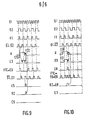
- FIG. 9 shows the case where signal A takes the value "1" at time t20. This has the effect of unlocking the assembly formed by the doors 430 and 434 so that the rising edge of the signal is transmitted by the door 430.
- the signal E3, output signal of the door 430 opens the door 436 so that the next pulse of signal D1.D2 is transmitted, via gates 436, 414 and 410, as reset pulse of up-down counter 400 (signal E5 and RZ).
- Signal A then takes the value "0" at time t22 which also results in the value "0” for signal E3.
- the mounting of doors 430 and 434 is blocked and the signal D1.D2 is no longer transmitted.
- the signal E5 has the value "0", and does not intervene in this case. It is not the same when the signal R takes the value “1” (see FIG. 10) at time t30, which causes the signal E5 to be set to “1” at time t31 at the next rising edge of the FT signal.
Landscapes
- Engineering & Computer Science (AREA)
- Computer Networks & Wireless Communication (AREA)
- Signal Processing (AREA)
- Mobile Radio Communication Systems (AREA)
- Transmitters (AREA)
Applications Claiming Priority (2)
| Application Number | Priority Date | Filing Date | Title |
|---|---|---|---|
| FR8315611A FR2552957B1 (fr) | 1983-09-30 | 1983-09-30 | Poste emetteur-recepteur pour un systeme de transmission d'informations par evasion de frequences |
| FR8315611 | 1983-09-30 |
Publications (3)
| Publication Number | Publication Date |
|---|---|
| EP0136757A2 EP0136757A2 (fr) | 1985-04-10 |
| EP0136757A3 EP0136757A3 (OSRAM) | 1985-06-12 |
| EP0136757B1 true EP0136757B1 (fr) | 1988-01-27 |
Family
ID=9292708
Family Applications (1)
| Application Number | Title | Priority Date | Filing Date |
|---|---|---|---|
| EP84201334A Expired EP0136757B1 (fr) | 1983-09-30 | 1984-09-14 | Poste émetteur-récepteur pour un système de transmission d'informations par évasion de fréquences |
Country Status (7)
| Country | Link |
|---|---|
| US (1) | US4606040A (OSRAM) |
| EP (1) | EP0136757B1 (OSRAM) |
| AU (1) | AU564721B2 (OSRAM) |
| CA (1) | CA1232019A (OSRAM) |
| DE (1) | DE3469121D1 (OSRAM) |
| FR (1) | FR2552957B1 (OSRAM) |
| IL (1) | IL73095A (OSRAM) |
Families Citing this family (22)
| Publication number | Priority date | Publication date | Assignee | Title |
|---|---|---|---|---|
| EP0137963B1 (en) * | 1983-09-16 | 1988-09-28 | Stauffer Chemical Company | Certain 2-(2-substituted benzoyl)-1,3-cyclohexanediones |
| US4677617A (en) * | 1985-10-04 | 1987-06-30 | Hughes Aircraft Company | Rapid frequency-hopping time synchronization |
| CH671124A5 (OSRAM) * | 1986-04-30 | 1989-07-31 | Zellweger Uster Ag | |
| US4694467A (en) * | 1986-07-03 | 1987-09-15 | Signatron, Inc. | Modem for use in multipath communication systems |
| US5040189A (en) * | 1987-01-12 | 1991-08-13 | Motorola, Inc. | Multiple frequency radio system employing pulse repeaters |
| US4776012A (en) * | 1987-04-17 | 1988-10-04 | Unisys Corporation | Method of jumping composite PN codes |
| US5311542A (en) * | 1990-09-19 | 1994-05-10 | Honeywell Inc. | Spread spectrum communication system |
| US5235613A (en) * | 1992-03-02 | 1993-08-10 | The Boeing Company | Frequency hopping method and apparatus |
| GB2313984B (en) * | 1993-06-02 | 1998-01-28 | Vtech Communications Ltd | Interface protocol method and apparatus |
| DE4323376A1 (de) * | 1993-07-13 | 1995-01-19 | Abb Patent Gmbh | Verfahren und Einrichtung zur störsicheren bidirektionalen Informationsübertragung über Stromversorgungsnetze |
| US5598471A (en) * | 1993-11-16 | 1997-01-28 | South African Microelectronic Systems Ltd. | Method and apparatus for encoding and decoding of audio transmission signals |
| US6292508B1 (en) * | 1994-03-03 | 2001-09-18 | Proxim, Inc. | Method and apparatus for managing power in a frequency hopping medium access control protocol |
| US5923702A (en) * | 1996-06-10 | 1999-07-13 | Breeze Wireless Communications Ltd. | Frequency hopping cellular LAN system |
| DE19623279C1 (de) * | 1996-06-11 | 1997-12-11 | Nokia Mobile Phones Ltd | Schnurloses Telekommunikationsverfahren |
| US5860060A (en) * | 1997-05-02 | 1999-01-12 | Texas Instruments Incorporated | Method for left/right channel self-alignment |
| BR9714816A (pt) * | 1997-08-14 | 2000-10-03 | Siemens Ag | Processo e dispositivo para a geração de uma sequência de frequência portadora |
| US7280580B1 (en) | 1999-10-15 | 2007-10-09 | Telefonaktlebolaget Lm Ericsson (Publ.) | Hop sequence adaptation in a frequency-hopping communications system |
| US7027424B1 (en) | 2000-05-24 | 2006-04-11 | Vtech Communications, Ltd. | Method for avoiding interference in a digital communication system |
| US7379447B2 (en) * | 2003-05-02 | 2008-05-27 | Microsoft Corporation | Slotted seeded channel hopping for capacity improvement in wireless networks |
| US7693488B2 (en) * | 2004-09-30 | 2010-04-06 | Vtech Telecommunications Limited | System and method for asymmetric enhanced mode operation in a digital communication system |
| EP4075680A1 (en) * | 2021-04-14 | 2022-10-19 | Renishaw PLC | Radio communications module for a measurement system |
| EP4075679A1 (en) | 2021-04-14 | 2022-10-19 | Renishaw PLC | Radio communications apparatus for a measurement system |
Family Cites Families (6)
| Publication number | Priority date | Publication date | Assignee | Title |
|---|---|---|---|---|
| US4383323A (en) * | 1980-06-09 | 1983-05-10 | Bell Telephone Laboratories, Incorporated | Spread spectrum FH-MFSK transmitter and receiver |
| DE3129911C2 (de) * | 1981-07-29 | 1987-03-05 | Siemens AG, 1000 Berlin und 8000 München | Pseudozufallsgenerator |
| FR2518338A1 (fr) * | 1981-12-15 | 1983-06-17 | Thomson Csf | Procede de synchronisation des postes emetteurs-recepteurs d'un reseau a sauts de frequence et poste destine a la mise en oeuvre de ce procede |
| US4558453A (en) * | 1981-12-16 | 1985-12-10 | Harris Corporation | Synchronization method and frequency hopping communication system |
| US4538281A (en) * | 1982-05-06 | 1985-08-27 | Rockwell International Corporation | Adaptive acquisition of multiple access codes |
| US4434504A (en) * | 1982-06-10 | 1984-02-28 | Frederickson Communications, Inc. | Channeling and decode circuit for airborne radio-telephone systems |
-
1983
- 1983-09-30 FR FR8315611A patent/FR2552957B1/fr not_active Expired
-
1984
- 1984-09-14 EP EP84201334A patent/EP0136757B1/fr not_active Expired
- 1984-09-14 DE DE8484201334T patent/DE3469121D1/de not_active Expired
- 1984-09-20 US US06/652,551 patent/US4606040A/en not_active Expired - Lifetime
- 1984-09-26 IL IL73095A patent/IL73095A/xx not_active IP Right Cessation
- 1984-09-27 CA CA000464195A patent/CA1232019A/en not_active Expired
- 1984-09-28 AU AU33660/84A patent/AU564721B2/en not_active Ceased
Also Published As
| Publication number | Publication date |
|---|---|
| EP0136757A2 (fr) | 1985-04-10 |
| AU564721B2 (en) | 1987-08-20 |
| IL73095A (en) | 1988-12-30 |
| FR2552957A1 (fr) | 1985-04-05 |
| US4606040A (en) | 1986-08-12 |
| FR2552957B1 (fr) | 1986-07-25 |
| EP0136757A3 (OSRAM) | 1985-06-12 |
| DE3469121D1 (en) | 1988-03-03 |
| CA1232019A (en) | 1988-01-26 |
| AU3366084A (en) | 1985-04-04 |
Similar Documents
| Publication | Publication Date | Title |
|---|---|---|
| EP0136757B1 (fr) | Poste émetteur-récepteur pour un système de transmission d'informations par évasion de fréquences | |
| FR2798810A1 (fr) | Procede et systeme de telecommunication en mode paquets dans lequel plusieurs communications sont transferables d'un chemin vers un autre | |
| FR2656447A1 (fr) | Dispositif de chronometrage de mobiles. | |
| EP0009096B1 (fr) | Procédé et système de synchronisation d'un réseau de communication à accès multiple par répartition dans le temps et utilisant un satellite ayant plusieurs antennes à faisceau directif sur des fréquences différentes | |
| EP0113307A1 (fr) | Circuit d'alignement de blocs d'informations numériques de longueur fixe | |
| FR2508742A1 (fr) | Circuit pour synchroniser le fonctionnement d'un emetteur et d'un ou plusieurs recepteurs radioelectriques | |
| EP0171789A1 (fr) | Dispositifs de synchronisation de trame | |
| FR2461411A1 (fr) | Systeme de transmission de donnees utilisant les principes d'etalement du spectre | |
| EP0920157A1 (fr) | Dispositif de gestion de mémoire tampon partagée | |
| EP0033672B1 (fr) | Dispositif d'aiguillage de données numériques | |
| FR2617657A1 (fr) | Systeme de transmission de series d'echantillons numeriques codes par des mots binaires a longueurs variables | |
| EP0037299B1 (fr) | Dispositif de synchronisation d'informations numériques transmises par paquets | |
| FR2466921A1 (fr) | Appareil d'affectation et de selection de parties de canaux de transmission de donnees | |
| EP0454249B1 (fr) | Dispositif de commutation dynamique pour le masquage d'erreurs dans un système à doublement du conduit numérique | |
| EP0454246B1 (fr) | Dispositif de mise en phase de signaux dans un système à doublement du conduit numérique | |
| EP0082054B1 (fr) | Procédé de synchronisation des postes émetteurs-récepteurs d'un réseau à sauts de fréquence, et poste destiné à la mise en oeuvre de ce procédé | |
| EP0056208B1 (fr) | Procédé et dispositif de synchronisation de messages | |
| FR2728422A1 (fr) | Systeme de radio-communication permettant de gerer des retards de transmission variables | |
| EP0932112A1 (fr) | Lecteur de carte à puce muni d'un commutateur d'horloge | |
| FR2517145A1 (fr) | Circuit diviseur a rapport reglable et synthetiseur de frequence | |
| EP0373067B1 (fr) | Dispositif de synchronisation de l'émission et de la réception d'une station d'un réseau de communication notamment pour véhicule automobile | |
| EP0100523B1 (fr) | Procédé pour la transmission d'informations sur un canal d'échanges unique et application de ce procédé notamment à des dispositifs formant un système d'alarme | |
| EP0328448B1 (fr) | Procédé et dispositif de synchronisation entre des terminaux communiquant par l'intermédiaire d'une chaîne n'assurant pas la transparence temporelle | |
| EP0011540A1 (fr) | Dispositif d'interface entrée-sortie entre un commutateur de données et une pluralité de voies de transmission | |
| FR2721463A1 (fr) | Système de transmission comportant au moins deux liaisons pour relier un émetteur et un récepteur et récepteur convenant à un tel système. |
Legal Events
| Date | Code | Title | Description |
|---|---|---|---|
| PUAI | Public reference made under article 153(3) epc to a published international application that has entered the european phase |
Free format text: ORIGINAL CODE: 0009012 |
|
| AK | Designated contracting states |
Designated state(s): DE FR GB IT NL SE |
|
| PUAL | Search report despatched |
Free format text: ORIGINAL CODE: 0009013 |
|
| AK | Designated contracting states |
Designated state(s): DE FR GB IT NL SE |
|
| RTI1 | Title (correction) | ||
| 17P | Request for examination filed |
Effective date: 19850801 |
|
| 17Q | First examination report despatched |
Effective date: 19860710 |
|
| GRAA | (expected) grant |
Free format text: ORIGINAL CODE: 0009210 |
|
| AK | Designated contracting states |
Kind code of ref document: B1 Designated state(s): DE FR GB IT NL SE |
|
| REF | Corresponds to: |
Ref document number: 3469121 Country of ref document: DE Date of ref document: 19880303 |
|
| ITF | It: translation for a ep patent filed | ||
| GBT | Gb: translation of ep patent filed (gb section 77(6)(a)/1977) | ||
| PLBE | No opposition filed within time limit |
Free format text: ORIGINAL CODE: 0009261 |
|
| STAA | Information on the status of an ep patent application or granted ep patent |
Free format text: STATUS: NO OPPOSITION FILED WITHIN TIME LIMIT |
|
| 26N | No opposition filed | ||
| PGFP | Annual fee paid to national office [announced via postgrant information from national office to epo] |
Ref country code: FR Payment date: 19910913 Year of fee payment: 8 |
|
| PG25 | Lapsed in a contracting state [announced via postgrant information from national office to epo] |
Ref country code: FR Effective date: 19930528 |
|
| REG | Reference to a national code |
Ref country code: FR Ref legal event code: ST |
|
| ITTA | It: last paid annual fee | ||
| EAL | Se: european patent in force in sweden |
Ref document number: 84201334.4 |
|
| ITPR | It: changes in ownership of a european patent |
Owner name: CAMBIO RAGIONE SOCIALE;PHILIPS ELECTRONICS N.V. |
|
| NLT1 | Nl: modifications of names registered in virtue of documents presented to the patent office pursuant to art. 16 a, paragraph 1 |
Owner name: PHILIPS ELECTRONICS N.V. |
|
| PGFP | Annual fee paid to national office [announced via postgrant information from national office to epo] |
Ref country code: GB Payment date: 19970829 Year of fee payment: 14 |
|
| PGFP | Annual fee paid to national office [announced via postgrant information from national office to epo] |
Ref country code: SE Payment date: 19970925 Year of fee payment: 14 |
|
| PGFP | Annual fee paid to national office [announced via postgrant information from national office to epo] |
Ref country code: NL Payment date: 19970930 Year of fee payment: 14 |
|
| PGFP | Annual fee paid to national office [announced via postgrant information from national office to epo] |
Ref country code: DE Payment date: 19971121 Year of fee payment: 14 |
|
| PG25 | Lapsed in a contracting state [announced via postgrant information from national office to epo] |
Ref country code: GB Free format text: LAPSE BECAUSE OF NON-PAYMENT OF DUE FEES Effective date: 19980914 |
|
| PG25 | Lapsed in a contracting state [announced via postgrant information from national office to epo] |
Ref country code: SE Free format text: LAPSE BECAUSE OF NON-PAYMENT OF DUE FEES Effective date: 19980915 |
|
| PG25 | Lapsed in a contracting state [announced via postgrant information from national office to epo] |
Ref country code: NL Free format text: LAPSE BECAUSE OF NON-PAYMENT OF DUE FEES Effective date: 19990401 |
|
| GBPC | Gb: european patent ceased through non-payment of renewal fee |
Effective date: 19980914 |
|
| EUG | Se: european patent has lapsed |
Ref document number: 84201334.4 |
|
| NLV4 | Nl: lapsed or anulled due to non-payment of the annual fee |
Effective date: 19990401 |
|
| PG25 | Lapsed in a contracting state [announced via postgrant information from national office to epo] |
Ref country code: DE Free format text: LAPSE BECAUSE OF NON-PAYMENT OF DUE FEES Effective date: 19990701 |