EP0136757B1 - Transceiver station for a frequency hopping information transmission system - Google Patents
Transceiver station for a frequency hopping information transmission system Download PDFInfo
- Publication number
- EP0136757B1 EP0136757B1 EP84201334A EP84201334A EP0136757B1 EP 0136757 B1 EP0136757 B1 EP 0136757B1 EP 84201334 A EP84201334 A EP 84201334A EP 84201334 A EP84201334 A EP 84201334A EP 0136757 B1 EP0136757 B1 EP 0136757B1
- Authority
- EP
- European Patent Office
- Prior art keywords
- code
- signal
- transceiver station
- law
- counter
- Prior art date
- Legal status (The legal status is an assumption and is not a legal conclusion. Google has not performed a legal analysis and makes no representation as to the accuracy of the status listed.)
- Expired
Links
Images

Classifications
-
- H—ELECTRICITY
- H04—ELECTRIC COMMUNICATION TECHNIQUE
- H04B—TRANSMISSION
- H04B1/00—Details of transmission systems, not covered by a single one of groups H04B3/00 - H04B13/00; Details of transmission systems not characterised by the medium used for transmission
- H04B1/69—Spread spectrum techniques
- H04B1/713—Spread spectrum techniques using frequency hopping
- H04B1/7143—Arrangements for generation of hop patterns
-
- H—ELECTRICITY
- H04—ELECTRIC COMMUNICATION TECHNIQUE
- H04B—TRANSMISSION
- H04B1/00—Details of transmission systems, not covered by a single one of groups H04B3/00 - H04B13/00; Details of transmission systems not characterised by the medium used for transmission
- H04B1/69—Spread spectrum techniques
- H04B1/713—Spread spectrum techniques using frequency hopping
- H04B1/7156—Arrangements for sequence synchronisation
- H04B2001/71563—Acquisition
Definitions
- the invention relates to a transceiver station for a system for transmitting information by frequency evasion, comprising a code generator for defining the operation of a plurality of channels according to a law known as the law of rapid jumps for a transmitter station -receiver in transmission position or in reception position and according to a law called slow jump law for a transceiver station in standby position, the law of fast jumps consisting in the operation of each of the channels for a time Tp.
- a code generator for defining the operation of a plurality of channels according to a law known as the law of rapid jumps for a transmitter station -receiver in transmission position or in reception position and according to a law called slow jump law for a transceiver station in standby position, the law of fast jumps consisting in the operation of each of the channels for a time Tp.
- This second described measure already implies a first drawback due to the necessity of the call sequence formed by the synchronization word repeating on different stages. Indeed, it is then impossible for a transceiver station which has not captured this sequence to participate in the communication of the transceiver station having launched this sequence.
- a second drawback is due to the fact that the duration of silence must be measured, which implies that means must be provided for measuring it and, in addition, means for changing the law of slow jumps as and when that this duration becomes important.
- the present invention provides a transceiver station of the kind mentioned above which does not have these drawbacks.
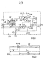
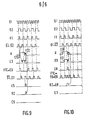
- Frequency evasion transmission systems use a plurality of frequency channels; these channels bear the references CF1 to CF12 in FIG. 1.
- Each of these channels is used for a time Tp according to a law known as the law of rapid jumps; thus in FIG. 1 a, the channels CFB, CF7, CF11, CF4, CF3, CF10, CF5, CF2, CF9, CF6, CF12, CF2, etc. are successively exploited. From this law of rapid jumps, a law is defined. slow jumps.
- S1, S2 we take successions S1, S2; .. of five channels.
- In each of these successions we take a median channel: CF11 for S1, CF2 for S2 ...
- the law of slow jumps consists in taking these median channels for a duration 5Tp as shown in Figure 1b.
- the middle channel of the fast jump law corresponds to the middle of the channel of the slow jump law.
- a guard time Tg is provided before the channel is actually used after a channel change (see FIG. 2).
- FIG. 3 the distribution of the binary elements transmitted by a median channel during the duration Tp is shown.
- a series of RO bearings which is an alternating series of “1” and “0” binary, is transmitted in order to facilitate the synchronization of the clock, at the frequency of appearance of the binary elements ; after this sequence, the synchronization code word MS is transmitted, then finally the rest of the time the useful bits of information: 1 N F.
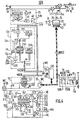
- FIG. 4 represents a transceiver station in accordance with the invention.
- An antenna 10 is used both for transmission and for reception. This antenna is therefore connected either to the output of a transmission modulator 12 or to the input of a receiver 14, this choice being determined by the position of a switch 16.
- the modulator 12 allows the data present on a terminal 18 to be transmitted on a channel whose frequency is determined by a frequency synthesizer 20.
- This frequency synthesizer is also used by the receiver 14 to fix the frequency of the first local oscillator. This frequency, with respect to the transmission frequency, is offset by a value equal to that of the intermediate frequency Fi.
- a switch 22 makes it possible to switch the output frequency of the synthesizer 20 either to the transmission modulator 12 or to the receiver 14.
- a command 24 is provided to shift the value from Fi of the output frequency of the synthesizer 20.
- a blocking command 26 makes it possible to cancel the output signal of the synthesizer 20 during the guard time Tg.
- a terminal 30 allows the user to process the data supplied by the receiver 14.
- a synchronization code recognition circuit 35 is formed by a shift register 40 to which a decoder 42 is attached. This register is filled with data coming from the output of the receiver 14 at the rate of a synchronized clock 44, in particular by means of the sequence RO, at the frequency of appearance of the binary elements.
- the code MS is contained in full in the register 40, it is then recognized by the decoder 42 which supplies an active signal (see in line 3 the line (MS)).
- This active signal is delayed by a time Tp 'by means of a delay circuit 46 before being applied to the trigger input of a monostable circuit 48 with retriggering.
- This time Tp corresponds to the end of the use of the channel.
- the switching period of the monostable circuit 48 is slightly greater than the period of appearance of the signal MS so that at the output of the circuit 48, there appears a logic signal SYN taking the logic value "1" at the end of the operation. of a channel that transmitted the MS code.
- the SYN signal remains at this logic level "1 as long as this code is regularly received.
- the synthesizer 20 is provided with a code entry 50.
- the code present at this entry must be validated by the transition of a signal SF to be able to determine the frequency of the output signal of this synthesizer 20.
- These codes come from a code generator 55 which is of the pseudo-random sequence type, for example. The rate of appearance of these codes is fixed by a signal FA developed by means of a quartz time base 60; at each rising edge of the signal FA, a new code appears at the output of the generator 55 for a time fixed by a short pulse of a signal WE. Outside this time the generator output is at high impedance.
- the generator 55 supplies, as shown in FIG. 1 a, successively the codes ... D- 2 , D -1 , DO, +1 , D +2 , E- 2 , E '1' EO, E +1 , E +2 , F -2 , F -1 , ...
- a position logic circuit bearing the reference 70 provides different signals defining the different positions that the transceiver station can take. These positions are mainly determined by means of an E / R command which appears, in FIG. 4, in the form of a switch applying a logic "1" to the input of a D type flip-flop, carrying the reference 72, for the transmission position and a logical "0" for the reception position.
- the reception position a distinction is made between the active reception position, that is to say that the station is in operation according to the law of fast jumps, and the standby position in this case the station is in operation according to the law of slow jumps, the transition from the law of slow jumps to the law of fast jumps being triggered when the SYN signal takes the value "1".
- the clock input of flip-flop 72 receives the signal FA.
- the signal Em which appears at the output Ou of the flip-flop 72 controls in particular the position of the switches 16, 22 and that of the switch 24, the signal Em at the output Q of the flip-flop 72 is used, inter alia, to develop d firstly the signal RA which, when it has the value "1", means that the set is in the active reception position and secondly the signal VE which, when it has the value "1", means that the extension is in standby position.
- the signal RA is produced by means of an AND gate 74 which receives on one of its inputs the signal Em and on the other the signal SYN while the signal VE appears at the output of another AND gate 76 receiving on the one of its inputs the signal Em and on the other the signal SYN.
- the first requirement which is imposed is that, when the station goes on transmission, the code which must be applied to the inputs 50 at the next rising edge of the FA signal is the one which would be transmitted if the station had remained, since the initialization of generator 55, in transmission position.
- the second requirement is that as soon as the synchronization word is received (this happens, in principle, only in the median channels) the receiver must listen on the posterior channel following the median channel and thus pass to the law of fast jumps .
- a memory device 100 has been provided to which a write circuit 110 is attached to write therein at the rate of the fast jump law the codes provided by the generator 55 and a read circuit 120 to take there the code intended to fix the frequency channel according to the position of the transceiver station and the reception of the synchronization code.
- the line (100) represents the locations of the memories with the code they contain.
- the hatched boxes indicate the entry of a new code.
- the read circuit 120 providing a read address code RADR comprises a register 200 which permanently contains the address code ad0, that is to say the address of the middle channel. This code passes through a switch 222 in position "ve" before being applied to input 150 of memory 100.
- the listening channel is always the middle channel so that the transceiver station is in position standby with the law of slow jumps.
- the reading code comes from a counter 250; when the transceiver station is in the transmit position this counter increments by one on each active edge of the FA signal and when it is in the receive position (fast jumps) on each rising edge of a Cp signal which will be question thereafter, this choice being made by means of a switch 252 controlled by the signal Em.
- a relationship is imposed between the write address code WADR and the code d RADR read address.
- the counter 250 is initialized on passing to "1" of the signal Em; the WADR code is reduced by two units by means of a subtraction member 255; then this code is applied to the parallel inputs counter 250 via a switch 260 set to "wm” by the signal Em taking the value "1)).
- a pulse trainer 262 provides a pulse to the load control input of counter 250. This load pulse is triggered by the transition from "0" to "1". of the value of the signal Em transmitted by an “OR” gate 265.
- the read circuit 120 includes another register 270 which contains the address code "ad1"; this code is intended to be loaded into the counter 250 when the switch 260 is in its other position and when the output pulse from the formatter 262 is triggered by the change to "1" of the signal RA.
- the transceiver station shown in FIG. 4 finally comprises a leveling management circuit 300 which cooperates with the time base 60.
- This management circuit is formed from a counter 305 provided with an input for counting signals connected to the output of an “AND” gate 307 and of a reset input connected to the output of an “OR” gate 310. It is at the output of this gate 310 that the signal Cp is supplied .
- To this counter 305 are added four decoders 311, 312, 313, 314.
- the decoder 311 supplies the signal SF for minimum content; the decoder 312 supplies an active signal when the counter 305 reaches its maximum position, the frequency of the increment signals being such that the time taken by the counter 305 to reach its maximum position starting from its initial position corresponds to the time Tp; the decoder 313, used for a variant of the invention, provides a signal TM whose transition to the active state should correspond to the transition to the active state of the signal MS and the decoder 314 provides an active signal corresponding to the end of the guard time Tg. This last signal is applied to the input S of an RS type flip-flop bearing the reference 320 while the input R is connected to the output of the “OR” gate 310.
- the signal BL is taken which opens the switch 26 during Tg and then closes it.
- the output of the decoder 312 is connected on the one hand to the input of an “AND” gate 322 with two inputs, the other input of which receives the signal VE by means of a logic signal inverter 323 and d on the other hand at the input of an “AND” gate 324 with two inputs also, the other input of which directly receives the signal VE.
- the output of door 322 is connected to one of the two inputs of door "OR” 310 while the output of door 324 is connected to one of the two inputs of door 307 via a logic signal inverter 327.
- the other input of gate 307 is connected either directly to the output of time base 60 to receive an FT signal according to a first variant 1 of the invention, or to the output of a circuit regulator 350 according to the preferred embodiment variant II of the invention, which has been discussed.
- This circuit 350 will be described later in this memo.
- the "OR" gate 310 receives a signal from a pulse trainer 352 triggered by the output signal from an "OR” gate 354 provided with three inputs. One of these inputs receives the signal Em, the other, the signal RA and the third, the output signal from a gate 355 of which one of the two inputs receives the signal VE and the other a signal AO produced by a 360 decoder attached to counter 122. This 360 decoder provides an active signal when the address code "adO" appears inside counter 122.
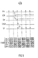
- FIG. 5 represents the case where from the standby position the E / R command is operated to switch to the transmission position.
- the switch 222 In the standby position, the switch 222 is in its “ve” position so that the RADR code is the “adO” code contained in the register 200, the code contained at this location in the memory 100 is validated by the signal SF which occurs at the start of the guard time Tg; in the standby position, this guard time only appears on each code change at the “adO” address.
- This change detected by the decoder 360 causes via the ports 355, 354, the formatter 352 and the gate 310, a reset pulse of the counter 305 and the zero setting of the flip-flop 320.
- the counter 305 counts fast pulses of the time base 60 then the signal SF appears, which validates the new code coming from the location "adO" of the memory 100 for the synthesizer, then the counter arrives at a content corresponding to the time Tg, the flip-flop 320 is set to “1” which closes the switch 26. Finally, the counter reaches its maximum position, it is then blocked since on the one hand, the door 322 is closed therefore the door 310 cannot supply a reset pulse and on the other hand, the door 307 is also closed by the output signal from the inverter 327 reflecting the fact that one is on standby and that the counter 305 is at its maximum position. To unblock the counter, you must therefore wait for the next appearance of the AO signal.
- the pulse trainer 352 which resets the counter 305 and sets the signal BL to the active state; counter 305 begins to count and soon supplies the signal SF which validates at time t3 the exit code from memory 100 corresponding to the address contained in counter 250; this address is defined by the code contained in the counter 122 reduced by two units then transferred to the counter 250 by the impulse provided by the trainer 262. This reduction is carried out "modulo 5" which corresponds to the number of em placement of memory 100. If we refer to line (100) we see the evolution of writing and reading of memory 100. Just before time t 1, we write in memory 100 the code D +1 ; switching to transmission does not disturb the memory write cycle in any way.
- the code DO is read since it is at the address "adO" while the writing code was “ad +2 ".
- the counter 250 will be incremented at the next zero crossing (signal Cp) of the counter 305 and the code D + i will be read at the location "ad +1 " the process then proceeds in the same manner. It can therefore be seen that the code which governs the frequency of the synthesizer 20 is systematically delayed by two codes with respect to the code generated by the generator 55.
- the synchronization word is contained in the register 40 which is detected by the decoder 42; this pulse delayed by the duration Tp 'puts the signal SYN in the logic "1" state and therefore also the signal RA.
- the pulse trainer 262 causes the counter 250 to be loaded so that the latter contains the code "ad1 coming from the register 270. Furthermore the counter 305 is set to zero which causes the first pulse Cp to arise at the instant t11 (figure 6). Although the counting input of counter 250 receives the signal Cp via the switch 252, this first pulse Cp has no influence on the content thereof, the loading command having priority over any other action.
- FIG. 6 shows in dotted lines, just like FIG. 5, the boxes of the codes read while the boxes of registered codes are hatched. At each rising edge of the signal FA, a code for the generator 55 is written and at each signal SF a code from the memory 100 is validated for the synthesizer 20.
- the signal SF only appears at a rising edge of the signal FT which causes the step counter 305 to increment, and therefore that the active transition only appears when D1 is equal to "1"; we then realize that there is no problem of reading and writing memory 100 simultaneously.
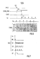
- this circuit modifies the rate of the counting signals of the counter 305. This modification is based on the instant of appearance of a particular code in time. transmission in a channel. In the context of the example described, this code is the MS code already used, this MS code must be recognized at the time TM counted from the start of the plateau. This time TM is determined in the transceiver station by means of the decoder 313, the regulation circuit 350 will therefore operate so that there is a coincidence in time between the appearance of the signal MS and that of the signal of TM output from decoder 313.
- This regulation circuit 350 consists of an up-down counter 400 to which two decoders 402 and 404 are attached; the decoder 402 supplies a signal A which, active, means that the appearance of MS is ahead of that of TM; the decoder 404 supplies a signal R which, active, means that the appearance of MS is lagging behind that of TM.
- the up-down counter 400 can be put in the up or down counting position by the output signal of an RS type flip-flop bearing the reference 406.
- the signal “1" of this flip-flop puts the up-down counter 400 in the up-counting position and the signal "0" in the down counting position.
- the flip-flop 406 is set to "1” by the sginal Cp and to "0" by the signal TM.
- the signal MS is applied to the up-down counting input to increment the up-down counter by “+1” or “-1” depending on whether one is up or down.
- the up-down counter 400 can be set to zero by the output signal from an "OR” gate 410, one of its two inputs of which receives the output signal from a pulse trainer 412 and the other an RZ signal.
- the input of the formatter 412 receives the SYN signal; the signal RZ comes from an “OR” gate bearing the reference 414.
- FIG. 9 shows the case where signal A takes the value "1" at time t20. This has the effect of unlocking the assembly formed by the doors 430 and 434 so that the rising edge of the signal is transmitted by the door 430.
- the signal E3, output signal of the door 430 opens the door 436 so that the next pulse of signal D1.D2 is transmitted, via gates 436, 414 and 410, as reset pulse of up-down counter 400 (signal E5 and RZ).
- Signal A then takes the value "0" at time t22 which also results in the value "0” for signal E3.
- the mounting of doors 430 and 434 is blocked and the signal D1.D2 is no longer transmitted.
- the signal E5 has the value "0", and does not intervene in this case. It is not the same when the signal R takes the value “1” (see FIG. 10) at time t30, which causes the signal E5 to be set to “1” at time t31 at the next rising edge of the FT signal.
Description
L'invention concerne un poste émetteur-récepteur pour un système de transmission d'informations par évasion de fréquences, comportant un générateur de codes pour définir l'exploitation d'une pluralité de canaux selon une loi dite loi de sauts rapides pour un poste émetteur-récepteur en position émission ou en position réception et selon une loi dite loi de sauts lents pour un poste émetteur-récepteur en position veille, la loi de sauts rapides consistant en l'exploitation de chacun des canaux pendant un temps Tp.The invention relates to a transceiver station for a system for transmitting information by frequency evasion, comprising a code generator for defining the operation of a plurality of channels according to a law known as the law of rapid jumps for a transmitter station -receiver in transmission position or in reception position and according to a law called slow jump law for a transceiver station in standby position, the law of fast jumps consisting in the operation of each of the channels for a time Tp.
La transmission d'informations par évasion de fréquences (mieux connue sous le nom anglo-saxon de FREQUENCY HOPPING) est utilisée notamment lorsqu'on souhaite transmettre des informations secrètes d'une manière sûre en évitant le brouillage éventuel des tiers mal intentionnés. Ce souhait est d'autant mieux exaucé que ladite loi de sauts rapides est compliquée c'est-à-dire que la séquence des codes élaborés par le générateur de codes est longue et le nombre de canaux de fréquences, élevé. Ceci présente des difficultés puisque pour qu'une transmission puisse avoir lieu il faut qu'il y ait une correspondance entre le canal utilisé du côté émission et le canal d'écoute du côté réception. Une première mesure que l'on prend pour surmonter cette difficulté consiste à caler, une fois pour toutes, tous les générateurs de code; ces générateurs calés restent alors toujours en fonctionnement.The transmission of information by evasion of frequencies (better known under the English name of FREQUENCY HOPPING) is used in particular when one wishes to transmit secret information in a safe way while avoiding the possible jamming of the malicious third parties. This wish is all the better fulfilled as the said law of rapid jumps is complicated, that is to say that the sequence of codes developed by the code generator is long and the number of frequency channels, high. This presents difficulties since for a transmission to take place there must be a correspondence between the channel used on the transmission side and the listening channel on the reception side. A first measure that we take to overcome this difficulty consists in stalling, once and for all, all the code generators; these stalled generators then always remain in operation.
Lorsque ce code de synchronisation est reçu par un poste émetteur-récepteur en position veille, s'impose alors une première exigence: il faut que le passage de la loi de saut lent à la loi de saut rapide se fasse le plus rapidement possible afin de faciliter le trafic. Pour s'assurer que le code de synchronisation soit bien reçu par le poste émetteur-récepteur en position veille, on s'impose du côté émission une deuxième exigence à savoir que le premier canal de la loi de sauts rapides utilisé par un poste qui passe de la position veille à la position émission doit être celui qui serait utilisé par ce même poste mis en position émission depuis l'opération de calage dont il a été question ci-dessus.When this synchronization code is received by a transceiver station in the standby position, there is a first requirement: the transition from the slow jump law to the fast jump law must take place as quickly as possible in order to facilitate traffic. To ensure that the synchronization code is received by the transceiver station in standby position, there is a second requirement on the transmission side, namely that the first channel of the law of rapid jumps used by a station which passes from the standby position to the transmission position must be the one that would be used by this same station put in the transmission position since the setting operation mentioned above.
Il est bien évident que ce calage initial n'est pas suffisant pour assurer cette correspondance, puisque d'une part une dérive inévitable des générateurs va survenir au cours du temps et que d'autre part les durées de propagation entre les différents postes émetteurs-récepteurs sont différentes; ainsi il peut même arriver qu'il n'y ait pas de recoupement entre les canaux du côté émission et du côté réception. Une deuxième mesure que l'on prend pour qu'un poste émetteur-récepteur puisse se synchroniser a été décrite dans la demande de brevet européen 0 082 054. Cette deuxième mesure consite, pour un poste émetteur-récepteur cherchant à établir une communication, à émettre des mots de synchronisation dans chaque palier de la loi de sauts rapides tandis que les postes émetteurs-récepteurs en attente sont soumis à une loi de sauts lents dont l'évolution est fixée par une durée de silence, cette durée du silence étant la durée pendant laquelle lesdits postes n'ont pas communiqué.It is obvious that this initial setting is not sufficient to ensure this correspondence, since on the one hand an inevitable drift of the generators will occur over time and on the other hand the propagation times between the different transmitting stations- receivers are different; thus it can even happen that there is no overlap between the channels on the transmission side and on the reception side. A second measure that is taken so that a transceiver station can synchronize has been described in European patent application 0 082 054. This second measure consists, for a transceiver station seeking to establish a communication, to send synchronization words in each level of the fast jump law while the waiting transceivers are subjected to a slow jump law whose evolution is fixed by a duration of silence, this duration of silence being the duration during which said posts did not communicate.
Cette deuxième mesure décrite implique déjà un premier inconvénient dû à la nécessité de la séquence d'appel formée du mot de synchronisation se répétant sur différents paliers. En effet, il est alors impossible pour un poste émetteur-récepteur qui n'a pas capté cette séquence de participer à la communication du poste émetteur-récepteur ayant lancé cette séquence. Un deuxième inconvénient est dû au fait qu'il faut mesurer la durée de silence, ce qui implique qu'il faut prévoir des moyens pour la mesurer et, en plus, des moyens pour faire évoluer la loi de sauts lents au fur et à mesure que cette durée devient importante.This second described measure already implies a first drawback due to the necessity of the call sequence formed by the synchronization word repeating on different stages. Indeed, it is then impossible for a transceiver station which has not captured this sequence to participate in the communication of the transceiver station having launched this sequence. A second drawback is due to the fact that the duration of silence must be measured, which implies that means must be provided for measuring it and, in addition, means for changing the law of slow jumps as and when that this duration becomes important.
La présente invention propose un poste émetteur-récepteur du genre mentionné ci-dessus qui ne présente pas ces inconvénients.The present invention provides a transceiver station of the kind mentioned above which does not have these drawbacks.
Pour cela, un tel poste est remarquable en ce qu'il comporte un dispositif de mémoire auquel sont rattachés d'une part un circuit d'écriture pour y emmagasiner au fur et à mesure les codes provenant du générateur et d'autre part un circuit de lecture pour y prélever les codes en fonction des positions du poste émetteur-récepteur:
- - en position émission et réception, pour établir la loi de sauts rapides,
- - en position veille pour établir la loi de sauts lents consistant en un changement de canaux d'écoute exploités pendant N x Tp correspondant chacun à un canal médian d'une succession de N canaux de ladite loi de sauts rapides, et des moyens pour inclure un code de synchronisation dans chaque canal médian.
- - in transmission and reception position, to establish the law of rapid jumps,
- in the standby position to establish the law of slow jumps consisting of a change in listening channels operated during N x Tp each corresponding to a median channel of a succession of N channels of said law of rapid jumps, and means for including a synchronization code in each median channel.
Une caractéristique de l'invention selon laquelle un poste émetteur-récepteur est remarquable en ce que le dispositif de mémoire est formé par une mémoire à accès direct ayant une capacité pour N codes tandis que le circuit d'écriture est un compteur modulo N s'incrémentant d'une unité à chaque code fourni par le générateur de code, en ce que le circuit de lecture prélève:
- - en position émission un code dont l'adresse en mémoire est définie à partir de code du compteur modulo N par une certaine relation,
- - en position veille un code à l'adresse du code définissant le canal médian,
- - en position réception le code à l'adresse supérieure d'une unité à l'adresse du code médian, dès que le signal en sortie d'un circuit de reconnaissance de code de synchronisation apparaît et successivement les codes rangés à des adresses successives de la mémoire, permet de satisfaire ces deux exigences.
- - in transmission position, a code whose address in memory is defined from the modulo N counter code by a certain relationship,
- - in standby position, a code at the address of the code defining the median channel,
- - in reception position, the code at the upper address of a unit at the address of the median code, as soon as the signal at the output of a synchronization code recognition circuit appears and successively the codes stored at successive addresses of memory enables these two requirements to be met.
La description suivante faite en regard des dessins annexés, le tout donné à titre d'exemple non limitatif, fera bien comprendre comment l'invention peut être réalisée.
- La figure 1 est un schéma qui illustre l'exploitation de canaux selon les lois dites: loi de sauts rapides et loi de sauts lents.
- La figure 2 montre la présence d'un temps de garde Tg entre chauqe changement de canal.
- La figure 3 montre la répartition des informations transmises sur chaque canal.
- La figure 4 montre un poste émetteur-récepteur conforme à l'invention.
- La figure 5 est un diagramme-temps illustrant le fonctionnement d'un poste émetteur-récepteur conforme à l'invention passant de la position veille à la position émission.
- La figure 6 est un diagramme-temps illustrant le fonctionnement d'un poste émetteur-récepteur conforme à l'invention passant de la position veille à la position réception.
- La figure 7 montre l'allure de quelques signaux utilisés pour fixer les temps d'inscription et les temps de lecture de la mémoire faisant partie du poste émetteur-récepteur de la figure 4.
- La figure 8 montre la constitution du circuit de régulation faisant partie, selon une variante de l'invention, du poste émetteur-récepteur de la figure 4.
- Les figures 9 et 10 sont des diagrammes-temps pour expliquer le fonctionnement du circuit de régulation dans le cas où il faut fournir des signaux à cadence plus lente et plus rapide respectivement.
- FIG. 1 is a diagram which illustrates the operation of channels according to the laws known as: law of fast jumps and law of slow jumps.
- Figure 2 shows the presence of a guard time Tg between each change of channel.
- Figure 3 shows the distribution of information transmitted on each channel.
- Figure 4 shows a transceiver station according to the invention.
- FIG. 5 is a time diagram illustrating the operation of a transceiver station in accordance with the invention passing from the standby position to the transmission position.
- FIG. 6 is a time diagram illustrating the operation of a transceiver station according to the invention passing from the standby position to the reception position.
- FIG. 7 shows the appearance of some signals used to fix the writing times and the reading times of the memory belonging to the transceiver station of FIG. 4.
- FIG. 8 shows the constitution of the regulation circuit forming part, according to a variant of the invention, of the transceiver station of FIG. 4.
- FIGS. 9 and 10 are time diagrams for explaining the operation of the regulation circuit in the case where it is necessary to supply signals with slower and faster cadences respectively.
Les systèmes de transmission par évasion de fréquence utilisent une pluralité de canaux de fréquence; ces canaux portent les références CF1 à CF12 à la figure 1. Chacun de ces canaux est utilisé pendant un temps Tp selon une loi dite loi de sauts rapides; ainsi à la figure 1 a on exploite successivement les canaux CFB, CF7, CF11, CF4, CF3, CF10, CF5, CF2, CF9, CF6, CF12, CF2 ... A partir de cette loi de sauts rapides, on définit une loi de sauts lents. Pour cet exemple on prend des successions S1, S2;.. de cinq canaux. Dans chacune de ces successions on prend un canal médian: CF11 pour S1, CF2 pour S2 ... La loi de sauts lents consiste à prendre ces canaux médians pendant une durée 5Tp comme cela est représenté à la figure 1 b. Le canal médian de la loi de sauts rapides correspond au milieu du canal de la loi de sauts lents.Frequency evasion transmission systems use a plurality of frequency channels; these channels bear the references CF1 to CF12 in FIG. 1. Each of these channels is used for a time Tp according to a law known as the law of rapid jumps; thus in FIG. 1 a, the channels CFB, CF7, CF11, CF4, CF3, CF10, CF5, CF2, CF9, CF6, CF12, CF2, etc. are successively exploited. From this law of rapid jumps, a law is defined. slow jumps. For this example we take successions S1, S2; .. of five channels. In each of these successions we take a median channel: CF11 for S1, CF2 for S2 ... The law of slow jumps consists in taking these median channels for a duration 5Tp as shown in Figure 1b. The middle channel of the fast jump law corresponds to the middle of the channel of the slow jump law.
Il convient de noter que le changement de canal ne s'effectue pas d'une manière instantanée; on prévoit un temps de garde Tg avant que le canal ne soit réellement utilisé après un changement de canal (voir figure 2).It should be noted that the channel change does not take place instantaneously; a guard time Tg is provided before the channel is actually used after a channel change (see FIG. 2).
A la figure 3, on a représenté la répartition des éléments binaires transmis par un canal médian pendant la durée Tp. Après le temps de garde Tg, une suite de roulements RO, qui est une suite alternée de «1 » et de «0» binaires, est transmise afin de faciliter la synchronisation de l'horloge, à la fréquence d'apparition des éléments binaires; après cette suite, on transmet le mot de code de synchronisation MS puis enfin le reste du temps les éléments binaires d'information utiles: 1 N F.In FIG. 3, the distribution of the binary elements transmitted by a median channel during the duration Tp is shown. After the guard time Tg, a series of RO bearings, which is an alternating series of “1” and “0” binary, is transmitted in order to facilitate the synchronization of the clock, at the frequency of appearance of the binary elements ; after this sequence, the synchronization code word MS is transmitted, then finally the rest of the time the useful bits of information: 1 N F.
La figure 4 représente un poste émetteur-récepteur conforme à l'invention. Une antenne 10 sert tant à l'émission qu'à la réception. Cette antenne est connectée donc, soit à la sortie d'un modulateur d'émission 12 soit à l'entrée d'un récepteur 14, ce choix étant déterminé par la position d'un commutateur 16. Le modulateur 12 permet à des données présentes sur une borne 18 d'être transmises sur un canal dont la fréquence est déterminée par un synthétiseur de fréquence 20. Ce synthétiseur de fréquence est aussi utilisé par le récepteur 14 pour fixer la fréquence du premier oscillateur local. Cette fréquence, par rapport à la fréquence d'émission, est décalée d'une valeur égale à celle de la fréquence intermédiaire Fi. Un commutateur 22 permet d'aiguiller la fréquence de sortie du synthétiseur 20 soit sur le modulateur d'émission 12 soit le récepteur 14. Lorsque le synthétiseur 20 est branché sur le récepteur 14, il est prévu une commande 24 pour décaler de Fi la valeur de la fréquence de sortie du synthétiseur 20. Une commande de blocage 26 permet d'annihilier le signal de sortie du synthétiseur 20 pendant le temps de garde Tg.FIG. 4 represents a transceiver station in accordance with the invention. An
Une borne 30 permet à l'utilisateur de traiter les données fournies par le récepteur 14. A cette borne est connecté un circuit de reconnaissance de code de synchronisation 35. Ce circuit est formé par un registre à décalage 40 auquel est rattaché un décodeur 42. Ce registre se remplit des données provenant de la sortie du récepteur 14 au rythme d'une horloge 44 synchronisée, notamment au moyen de la suite RO, à la fréquence d'apparition des éléments binaires. Lorsque le code MS est contenu en entier dans le registre 40, il est alors reconnu par le décodeur 42 qui fournit un signal actif (voir à la figure 3 la ligne (MS)). Ce signal actif est retardé d'un temps Tp' au moyen d'un circuit retardateur 46 avant d'être appliqué à l'entrée de déclenchement d'un circuit monostable 48 à redéclenchement. Ce temps Tp' correspond à la fin de l'utilisation du canal. La période de basculement du circuit monostable 48 est légèrement supérieure à la période d'apparition du signal MS de sorte qu'à la sortie du circuit 48, apparaît un signal logique SYN prenant la valeur logique «1 » à la fin de l'exploitation d'un canal qui a transmis le code MS. Le signal SYN reste à ce niveau logique «1 tant que ce code est régulièrement reçu.A terminal 30 allows the user to process the data supplied by the receiver 14. To this terminal is connected a synchronization code recognition circuit 35. This circuit is formed by a shift register 40 to which a decoder 42 is attached. This register is filled with data coming from the output of the receiver 14 at the rate of a
Le synthétiseur 20 est muni d'une entrée de code 50. Le code présent à cette entrée doit être validé par la transition d'un signal SF pour pouvoir déterminer la fréquence du signal de sortie de ce synthétiseur 20. Ces codes proviennent d'un générateur de codes 55 qui est du type, par exemple, à séquence pseudo-aléatoire. Le rythme d'apparition de ces codes est fixé par un signal FA élaboré au moyen d'une base de temps à quartz 60; à chaque front montant du signal FA apparaît un nouveau code à la sortie du générateur 55 pendant un temps fixé par une courte impulsion d'un signal WE. En dehors de ce temps la sortie du générateur est à haute impédance.The
Il convient de rappeler que les générateurs contenus dans tous les postes émetteurs-récepteurs faisant partie du même système de transmission par évasion de fréquence sont initialisés en même temps et sont maintenus ensuite en permanence à l'état de fonctionnement.It should be recalled that the generators contained in all the transceiver stations which are part of the same frequency evasion transmission system are initialized at the same time and are then permanently maintained in the operating state.
Les codes de ce générateur 55 définissent donc les canaux; parmi ces codes on distingue:
- - les codes DO, EO, FO ... qui déterminent les canaux médians
- - les codes D-2, D-1; E-2, E-1; F-2, F -1; ...qui déterminent les canaux antérieurs;
- - les codes D+i, D+2; E+i, E+2; ... qui déterminent les canaux postérieurs.
- - DO, EO, FO codes ... which determine the middle channels
- - codes D-2, D-1; E-2, E-1; F-2, F -1 ; ... which determine the anterior canals;
- - the codes D + i, D +2 ; E + i, E +2 ; ... which determine the posterior canals.
Ainsi, le générateur 55 fournit, comme cela est montré à la figure 1 a, successivement les codes ... D-2, D-1, DO, ![]()
![]()
Pour un poste en veille, régi donc par la loi de sauts lents, ce sont les codes ...DO, EO;.. qui vont fixer pendant 5Tp les canaux médians.For a station in standby, therefore governed by the law of slow jumps, these are the codes ... DO, EO; .. which will fix the median channels for 5Tp.
Un circuit de logique de position portant la référence 70 fournit différents signaux définissant les différentes positions que peut prendre le poste émetteur-récepteur. Ces positions sont déterminées principalement au moyen d'une commande E/R qui se présente, à la figure 4, sous la forme d'un commutateur appliquant un «1» logique à l'entrée d'une bascule de type D, portant la référence 72, pour la position émission et un «0» logique pour la postion réception. Dans la position réception on distingue la position réception active c'est-à-dire que le poste est en exploitation selon la loi de sauts rapides, et la position veille dans ce cas le poste est en exploitation selon la loi de sauts lents, le passage de la loi de sauts lents à la loi de sauts rapides étant déclenché lorsque le signal SYN prend la valeur «1 ». L'entrée d'horloge de la bascule 72 reçoit le signal FA. Le signal Em qui apparaît à la sortie Ou de la bascule 72 commande notamment la position des commutateurs 16, 22 et celle de l'interrupteur 24, le signal Em à la sortie Q de la bascule 72 est utilisé, entre autres, pour élaborer d'une part le signal RA qui, lorsqu'il a la valeur «1 », signifie que le poste est en position réception active et d'autre part le signal VE qui, lorsqu'il a la valeur «1 », signifie que le poste est en position veille. Le signal RA est élaboré au moyen d'une porte ET 74 qui reçoit sur une de ses entrées le signal Em et sur l'autre le signal SYN tandis quele signal VE apparaît à la sortie d'une autre porte ET 76 recevant sur l'une de ses entrées le signal Em et sur l'autre le signal SYN.A position logic circuit bearing the reference 70 provides different signals defining the different positions that the transceiver station can take. These positions are mainly determined by means of an E / R command which appears, in FIG. 4, in the form of a switch applying a logic "1" to the input of a D type flip-flop, carrying the reference 72, for the transmission position and a logical "0" for the reception position. In the reception position a distinction is made between the active reception position, that is to say that the station is in operation according to the law of fast jumps, and the standby position in this case the station is in operation according to the law of slow jumps, the transition from the law of slow jumps to the law of fast jumps being triggered when the SYN signal takes the value "1". The clock input of flip-flop 72 receives the signal FA. The signal Em which appears at the output Ou of the flip-flop 72 controls in particular the position of the
La première exigence que l'on s'impose est que, lorsque le poste passe en émission, le code qui doit être appliqué aux entrées 50 au prochain front montant du signal FA est celui qui serait émis si le poste était resté, depuis l'initialisation du générateur 55, en position émission. La deuxième exigence est que dès que le mot de synchronisation est reçu (cela arrive, par principe, uniquement dans les canaux médians) le récepteur doit se mettre en écoute sur le canal postérieur suivant le canal médian et passer ainsi à la loi de sauts rapides.The first requirement which is imposed is that, when the station goes on transmission, the code which must be applied to the
Conformément à l'invention pour satisfaire ces exigences on a prévu un dispositif à mémoire 100 auquel sont rattachés un circuit d'écriture 110 pour y inscrire au rythme de la loi de sauts rapides les codes fournis par le générateur 55 et un circuit de lecture 120 pour y prélever le code destiné à fixer le canal de fréquence en fonction de la position du poste émetteur-récepteur et de la réception du code de synchronisation.In accordance with the invention, in order to satisfy these requirements, a
Le circuit d'écriture 110 fournissant des codes d'adresse d'écriture WADR est formé par un compteur 122 dont les positions de comptage correspondent chacune à une adresse de la mémoire 100. Ces adresses sont représentées symboliquement par ad-2, ad-1, ado, ad+1, ad+2. A chaque front montant du signal FA, le compteur 122 est incrémenté d'une unité. A partir de ce signal FA, la courte impulsion WE dont il a été question est élaborée, à l'intérieur de la base de temps 60, pour, d'une part, mettre la mémoire 100 en position d'écriture et pour, d'autre part, connecter son entrée de code d'adresse 150 sur les sorties en parallèle du compteur 122 par l'intermédiaire d'un commutateur 155. Les données à emmagasiner sont disponibles sur une ligne à plusieurs fils BUSD qui interconnecte la sortie du générateur 55, les accès de données de la mémoire 100 et les entrées 50 du synthétiseur 20. La sortie du générateur 55 étant à trois états, les données sont émises sur la ligne BUSD lorsque l'impulsion WE est active. Les codes fournis par le générateur 55 sont rangés successivement dans la mémoire 100 de la manière suivante:
- Le code DO est enregistré à l'adresse adO
- Le code D+1 est enregistré à l'adresse ad+1
- Le code D+2 est enregistré à l'adresse ad+z
- Le code E-2 est enregistré à l'adresse ad-2
- Le code E-1 est enregistré à l'adresse ad-1
- Le code EOest enregistré à l'adresse ad0 et ainsi de suite.
- DO code is registered at adO address
- The code D +1 is registered at the address ad +1
- The code D +2 is registered at the address ad + z
- The code E- 2 is registered at the address ad- 2
- The code E- 1 is registered at the address ad -1
- The EO code is saved at address ad0 and so on.
Aux figures 5 et 6 la ligne (100) représente les emplacements des mémoires avec le code qu'elles contiennent. Les cases hachurées indiquent l'inscription d'un code nouveau.In Figures 5 and 6 the line (100) represents the locations of the memories with the code they contain. The hatched boxes indicate the entry of a new code.
Le circuit de lecture 120 fournissant un code d'adresse de lecture RADR comporte un registre 200 qui contient en permanence le code d'adresse adO c'est-à-dire l'adresse du canal médian. Ce code transite par un commutateur 222 en position «ve» avant d'être appliqué à l'entré 150 de la mémoire 100. Ainsi le canal d'écoute est toujours le canal médian de sorte que le poste émetteur-récepteur se trouve en position veille avec la loi de sauts lents. Lorsque le poste émetteur-récepteur est en position réception avec les canaux d'écoute suivant la loi de sauts rapides, ou lorsqu'il est en position émission, le code de lecture provient d'un compteur 250; lorsque le poste émetteur-récepteur est en position émission ce compteur s'incrémente d'une unité à chaque front actif du signal FA et lorsqu'il est en position réception (sauts rapides) à chaque front montant d'un signal Cp dont il sera question par la suite, ce choix étant effectué par l'intermédiaire d'un commutateur 252 commandé par le signal Em. Lorsque le poste est en position émission, on impose une relation entre le code d'adresse d'écriture WADR et le code d'adresse de lecture RADR. Pour cela le compteur 250 est initialisé au passage à «1 » du signal Em; le code WADR est diminué de deux unités au moyen d'un organe de soustraction 255; puis ce code est appliqué aux entrées en parallèle du compteur 250 par l'intermédiaire d'un commutateur 260 mis en position «wm» par le signal Em prenant la valeur «1)). Un formateur d'impulsions 262 fournit une impulsion à l'entrée de commande de chargement du compteur 250. Cette impulsion de chargement est déclenchée par la transition de «0» à «1 ». de la valeur du signal Em transmise par une porte «OU» 265.The
Le circuit de lecture 120 comporte un autre registre 270 qui contient le code d'adresse «ad1 »; ce code est destiné à être chargé dans le compteur 250 lorsque le commutateur 260 est dans son autre position et lorsque l'impulsion de sortie du formateur 262 est déclenchée par le passage à «1 » du signal RA.The
Le poste émetteur-récepteur montré à la figure 4 comporte enfin un circuit de gestion de pallier 300 qui coopère avec la base de temps 60. Ce circuit de gestion est constitué à partir d'un compteur 305 muni d'une entrée pour signaux de comptage connectée à la sortie d'une porte «ET» 307 et d'une entrée de remise à zéro connectée à la sortie d'une porte «OU» 310. C'est à la sortie de cette porte 310 que le signal Cp est fourni. A ce compteur 305 sont adjoints quatre décodeurs 311, 312, 313, 314. Le décodeur 311 fournit le signal SF pou un contenu minimum; le décodeur 312 fournit un signal actif lorsque le compteur 305 atteint sa position maximum, la fréquence des signaux d'incrémentation étant telle que la durée que met le compteur 305 pour atteindre sa position maximale en partant de sa position initale correspond au temps Tp; le décodeur 313, utilisé pour une variante de l'invention, fournit un signal TM dont le passage à l'état actif devrait correspondre au passage à l'état actif du signal MS et le décodeur 314 fournit un signal actif correspondant à la fin du temps de garde Tg. Ce dernier signal est appliqué à l'entrée S d'une bascule de type RS portant la référence 320 tandis que l'entrée R est reliée à la sortie de la porte «OU» 310. A la sortie de la bascule 320, on prélève le signal BL qui ouvre l'in terrupteur 26 pendant Tg et le ferme ensuite. La sortie du décodeur 312 est reliée d'une part à l'entrée d'une porte «ET» 322 à deux entrées, dont l'autre entrée reçoit le signal VE par l'intermédiaire d'un inverseur de signaux logiques 323 et d'autre part à l'entrée d'une porte «ET» 324 à deux entrées aussi, dont l'autre entrée reçoit directement le signal VE. La sortie de la porte 322 est reliée à l'une des deux entrées de la porte «OU» 310 tandis que la sortie de la porte 324 est reliée à l'une des deux entrées de la porte 307 par l'intermédiaire d'un inverseur de signal logique 327. L'autre entrée de la porte 307 est reliée soit directement à la sortie de la base de temps 60 pour recevoir un signal FT selon une première variante 1 de l'invention, soit à la sortie d'un circuit de régulation 350 selon la variante Il de réalisation préférée de l'invention, dont il a été question. Ce circuit 350 sera décrit plus loin dans le présent mémoire. Outre le signal issu de la porte 322, la porte «OU» 310 reçoit un signal issu d'un formateur d'impulsions 352 déclenché par le signal de sortie d'une porte «OU» 354 munie de trois entrées. Une de ces entrées reçoit le signal Em, l'autre, le signal RA et la troisième, le signal de sortie d'une porte 355 dont l'une des deux entrées reçoit le signal VE et l'autre un signal AO élaboré par un décodeur 360 rattaché au compteur 122. Ce décodeur 360 fournit un signal actif à l'apparition, à l'intérieur du compteur 122, du code d'adresse «adO».The transceiver station shown in FIG. 4 finally comprises a
On explique maintenant le fonctionnement du poste émetteur-récepteur conforme à l'invention. Pour cela, on se rapporte, tout d'abord, à la figure 5 qui représente le cas où de la position veille on manoeuvre la commande E/R pour passer en position émission.The operation of the transceiver station according to the invention will now be explained. For this, we refer, first of all, to FIG. 5 which represents the case where from the standby position the E / R command is operated to switch to the transmission position.
En position de veille, le commutateur 222 est à sa position «ve» de sorte que le code RADR est le code «adO» contenu dans le registre 200, le code contenu à cet emplacement de la mémoire 100 est validé par le signal SF qui survient au début du temp de garde Tg; en position de veille, ce temps de garde n'apparaît qu'à chauqe changement de code à l'adresse «adO». Ce changement détecté par le décodeur 360 provoque via les ports 355, 354, le formateur 352 et la porte 310, une impulsion de remise à zéro du compteur 305 et la mise à zéro de la bascule 320. Le compteur 305 compte des impulsions rapides de la base de temps 60 puis le signal SF apparaît, qui valide le nouveau code issu de l'emplacement «adO» de la mémoire 100 pour le synthétiseur, puis le compteur arrive à un contenu correspondant au temps Tg, la bascule 320 est mise à «1 » ce qui ferme l'interrupteur 26. Enfin, le compteur atteint sa position maximale, il est alors bloqué puisque d'une part, la porte 322 est fermée donc la porte 310 ne peut pas fournir d'impulsion de remise à zéro et d'autre part, la porte 307 est aussi fermée par le signal de sortie de l'inverseur 327 traduisant le fait que l'on est en veille et que le compteur 305 est à sa position maximale. Pour débloquer le compteur il faut donc attendre la prochaine apparition du signal AO.In the standby position, the
Lorsqu'on veut passer en émission on manoeuvre la commande E/R de sorte qu'un «1 soit appliqué à l'entrée D de la bascule 72; en se reportant à la figure 5, cette manoeuvre a lieu au temps «t1 », le front montant du signal FA qui suit provoque au temps «t2» le passage de la valeur «0» à la valeur«1 » du signal em ce qui a pour effet de faire mettre en position «em» le commutateur 260 et de changer de position le commutateur 222 et surtour de déclencher l'impulsion de chargement fournie par le circuit 262 pour le compteur 250. Par ailleurs le passage à «1 » du signal em déclenche à l'intérieur du circuit de gestion de palier, le formateur d'impulsions 352 ce qui remet à zéro le compteur 305 et met à l'état actif le signal BL; le compteur 305 commence à comter et fournit bientôt le signal SF qui valide à l'instant t3 le code de sortie de la mémoire 100 correspondant à l'adresse contenue dans le compteur 250; cette adresse est définie par le code contenu dans le compteur 122 diminué de deux unités puis transféré dans le compteur 250 par l'impulsion fournie par le formateur 262. Ceete diminution s'effectue «modulo 5» ce qui correspond au nombre d'emplacement de la mémoire 100. Si on se rapporte à la ligne (100) on voit l'évolution de l'écriture et de la lecture de la mémoire 100. Juste avant l'instant t1, on inscrit dans la mémoire 100 le code D+1; le fait de passer en émission ne perturbe en rien le cycle d'écriture de la mémoire. Par contre à l'instant t3 où apparaît la transition active du signal S F le code DO est lu puisqu'il se trouve à l'adresse «adO» alors que le code d'écriture était «ad+2». Le compteur 250 sera incrémenté au prochain passage à zéro (signal Cp) du compteur 305 et le code D+i sera lu à l'emplacement «ad+1» le processus se déroule alors de la même manière. On constate donc que le code qui gouverne la fréquence du synthétiseur 20 est retardé systématiquement de deux codes par rapport au code engendré par le générateur 55.When one wants to pass in emission one maneuvers the command E / R so that a “1 is applied to the entry D of the rocker 72; referring to FIG. 5, this maneuver takes place at time "t1", the rising edge of the signal FA which follows causes at time "t2" the passage from the value "0" to the value "1" of the signal em ce which has the effect of placing the
On examine le cas où de la position veille le poste émetteur-récepteur passe en réception active c'est-à-dire que ce passage intervient dès que le mot MS est reçu. Ce cas est expliqué à l'aide de la figure 6.We examine the case where from the standby position the transceiver station goes into active reception, that is to say that this passage occurs as soon as the word MS is received. This case is explained using Figure 6.
On suppose qu'à l'instant t10 le mot de synchronisation est contenu dans le registre 40 ce qui est détecté par le décodeur 42; cette impulsion retardée de la durée Tp' met le signal SYN à l'état «1 logique et de ce fait le signal RA également. Le formateur d'impulsions 262 provoque le chargement du compteur 250 de sorte que celui-ci contienne le code «ad1 provenant du registre 270. Par ailleurs le compteur 305 est mis à zéro ce qui fait surgir la première impulsion Cp à l'instant t11 (figure 6). Bien que l'entrée de comptage du compteur 250 reçoive le signal Cp par l'intermédiaire du commutateur 252, cette première impulsion Cp est sans influence sur le contenu de celui-ci, la commande de chargement étant prioritaire sur tout autre action. Mais cette impulsion Cp de remise à zéro du compteur 305 fait surgir, peu de temps après, l'impulsion SF qui valide le code de sortie de la mémoire 100, ce code étant situé à l'adresse ad+i. Puis l'impulsion du formateur 262 disparaissant, la prochaine impulsion Cp incrémentera le compteur 250. La figure 6 montre en pointillé, tout comme la figure 5, les cases des codes lus tandis que les cases de codes inscrits sont hachurées. A chaque front montant du signal FA un code du générateur 55 est inscrit est à chauqe signal SF un code provenant de la mémoire 100 est validé pour le synthétiseur 20.It is assumed that at time t10 the synchronization word is contained in the register 40 which is detected by the decoder 42; this pulse delayed by the duration Tp 'puts the signal SYN in the logic "1" state and therefore also the signal RA. The
La figure 7 montre l'allure de signaux fournis par la base de temps 60. Ces signaux, tous périodiques, sont élaborés à partir d'un signal de fréquence élevée D1 égale ou supérieure à un multiple de la fréquence d'apparition des éléments binaires. A partir de D1 le signal D2 est obtenu après division par deux puis on réalise le signal FT tel que FT=D1.D2. Les signaux FA et WE ont des périodes égales à la durée du temps de palier, la largeur du temps où WE est actif est égale à la demi-période du signal D1 et ce signal est actif quand Dl =O. On remarquera que le signal SF n'apparaît qu'à un front montant du signal FT qui fait incrémenter le compteur de palier 305, et donc que la transition active n'apparaît que lorsque D1 est égal à «1»; on se rend alors compte qu'il n'y a aucun problème de lecture et d'écriture simultanées de la mémoire 100.FIG. 7 shows the appearance of signals supplied by the
A la figure 8, on a représenté le détail de réalisation du circuit de régulation 350. Ce circuit modifie la cadence des signaux de comptage du compteur 305. Cette modification est basée sur l'instant d'apparition d'un code particulier dans le temps de transmission dans un canal. Dans le cadre de l'exemple décrit ce code est le code MS utilisé déjà, ce code MS doit être reconnu au temps TM compté depuis le début du palier. Ce temps TM est déterminé dans le poste émetteur-récepteur au moyen du décodeur 313, le circuit de régulation 350 va donc oeuvrer pour qu'il y ait une coinci- dence dans le temps entre l'apparition du signal MS et celle du signal de sortie TM du décodeur 313.In FIG. 8, the detail of embodiment of the
Ce circuit de régulation 350 est constitué à partir d'un compteur-décompteur 400 auquel sont rattachés deux décodeurs 402 et 404; le décodeur 402 fournit un signal A qui, actif, signifie que l'apparition de MS est en avance sur celle de TM; le décodeur 404 fournit un signal R qui, actif, signifie que l'apparition de MS est en retard sur celle de TM.This
Le compteur-décompteur 400 peut être mis en position de comptage ou de décomptage par le signal de sortie d'une bascule de type RS portant la référence 406. Le signal «1» de cette bascule met le compteur-décompteur 400 en position de comptage et le signal «0» en position de décomptage. La bascule 406 est mise à «1» par le sginal Cp et à «0» par le signal TM. Le signal MS est appliqué à l'entrée de comptage-décomptage pour incrémenter de «+1» ou «-1» le compteur-décompteur selon que l'on est en comptage ou en décomptage. Le compteur-décompteur 400 peut être mis à zéro par le signal de sortie d'une porte «OU» 410 dont une de ses deux entrées reçoit le signal de sortie d'un formateur d'impulsions 412 et l'autre un signal RZ. L'entrée du formateur 412 reçoit le signal SYN; le signal RZ provient d'une porte «OU» portant la référence 414.The up-
Le signal FT dont on veut rajouter ou retrancher une impulsion selon que le signal A ou R est engendré est appliqué, d'une part, à l'une des deux entrées d'une porte 420 et, d'autre part, à l'une des deux entrées d'une porte 422. L'autre entrée de la porte 420 est reliée à la sortie d'une porte «OU» 426 dont une des deux entrées est reliée à la sortie de la porte 420 et l'autre à la sortie du décodeur 404. L'autre entrée de la porte 422 est reliée à la sortie d'une porte ET 430 par l'intermédiaire d'un inverseur de signaux logiques 432. Une des deux entrées de la porte 430 est reliée à la sortie d'une porte OU 434 munie de deux entrées. L'une est connectée à la sortie de la porte 430, l'autre, à la sortie du décodeur 402. La sortie de la porte 430 est reliée à l'une des entrées d'une porte ET 436 dont la sortie est reliée à l'une des deux entrées de la porte 414. Une porte «OU» à deux entrées 437 fournit le signal FTC qui est le signal FT corrigé que l'on applique selon cette variante Il à l'entrée d'incrémentation du compteur de palier 305. Les deuxièmes entrées des portes 414 et 420 sont connectées à la sortie d'une porte ET 425 dont une des deux entrées est connectée à la sortie de la porte 420. La deuxième entrée de la porte 437 est reliée à la sortie de la porte 422. Différents signaux intervenant dans le fonctionnement du circuit de régulation sont issus de la base de temps 60. Ce sont les signaux:
- D1. D2 qui sont appliqués à la deuxième entrée de la porte 430
- D1.D2 qui sont appliqués à la deuxième entrée de la
porte 436 - D1.D2 qui sont appliqués à la deuxième entrée de la
porte 426
- D1. D2 which are applied to the second entrance of gate 430
- D1.D2 which are applied to the second entrance of
gate 436 - D1.D2 which are applied to the second entrance of
gate 426
Pour expliquer le fonctionnement du circuit de régulation on fera appel aux signaux:
- E3 signal de sortie de la porte 430
- E5 signal de sortie de la
porte 436 - E8 signal de sortie de la porte 425
- E9 signal de sortie de la
porte 420.
- E3 output signal from gate 430
- E5 output signal from
gate 436 - E8 output signal from gate 425
- E9 output signal from
gate 420.
La figure 9 montre le cas où le signal A prend la valeur «1 » à l'instant t20. Ceci a pour effet de débloquer le montage formé par les portes 430 et 434 de sorte que le front montant du signal est transmis par la porte 430. Le signal E3, signal de sortie de la porte 430, ouvre la porte 436 de sorte que la prochaine impulsion du signal D1.D2 est transmise, via les portes 436, 414 et 410, comme impulsion de remise à zéro du compteur-décompteur 400 (signal E5 et RZ). Le signal A prend alors la valeur «0» à l'instant t22 ce qui entraîne aussi la valeur «0» pour le signal E3. Le montage des portes 430 et 434 est bloqué et le signal D1.D2 n'est plus transmis. Pendant le laps de temps où E3 avait la valeur «1» la porte 422 était bloqué; ainsi le signal FTC (FTC=E6) présente une impulsion en moins par rapport au signal FT. On notera que, pendant toutes ces opérations, le signal E5 a la valeur «0», et n'intervient pas dans ce cas. Il n'en est pas de même lorsque le signal R prend la valeur «1 » (voir la figure 10) à l'instant t30, ce qui provoque la mise à «1» » du signal E5 à l'instant t31 au prochain front montant du signal FT. Le signal E9 ayant la valeur «1» la porte E8 transmet via les portes 414 et 410 une impulsion de remise à zéro pour le compteur-décompteur 400 et insère dans les impulsions FT une impulsion supplémentaire. Dans ce cas FTC=E6+E8. On notera que E3 reste à zéro.FIG. 9 shows the case where signal A takes the value "1" at time t20. This has the effect of unlocking the assembly formed by the doors 430 and 434 so that the rising edge of the signal is transmitted by the door 430. The signal E3, output signal of the door 430, opens the
Claims (5)
Applications Claiming Priority (2)
| Application Number | Priority Date | Filing Date | Title |
|---|---|---|---|
| FR8315611 | 1983-09-30 | ||
| FR8315611A FR2552957B1 (en) | 1983-09-30 | 1983-09-30 | TRANSCEIVER STATION FOR A FREQUENCY ESCAPE INFORMATION TRANSMISSION SYSTEM |
Publications (3)
| Publication Number | Publication Date |
|---|---|
| EP0136757A2 EP0136757A2 (en) | 1985-04-10 |
| EP0136757A3 EP0136757A3 (en) | 1985-06-12 |
| EP0136757B1 true EP0136757B1 (en) | 1988-01-27 |
Family
ID=9292708
Family Applications (1)
| Application Number | Title | Priority Date | Filing Date |
|---|---|---|---|
| EP84201334A Expired EP0136757B1 (en) | 1983-09-30 | 1984-09-14 | Transceiver station for a frequency hopping information transmission system |
Country Status (7)
| Country | Link |
|---|---|
| US (1) | US4606040A (en) |
| EP (1) | EP0136757B1 (en) |
| AU (1) | AU564721B2 (en) |
| CA (1) | CA1232019A (en) |
| DE (1) | DE3469121D1 (en) |
| FR (1) | FR2552957B1 (en) |
| IL (1) | IL73095A (en) |
Families Citing this family (22)
| Publication number | Priority date | Publication date | Assignee | Title |
|---|---|---|---|---|
| EP0137963B1 (en) * | 1983-09-16 | 1988-09-28 | Stauffer Chemical Company | Certain 2-(2-substituted benzoyl)-1,3-cyclohexanediones |
| US4677617A (en) * | 1985-10-04 | 1987-06-30 | Hughes Aircraft Company | Rapid frequency-hopping time synchronization |
| CH671124A5 (en) * | 1986-04-30 | 1989-07-31 | Zellweger Uster Ag | |
| US4694467A (en) * | 1986-07-03 | 1987-09-15 | Signatron, Inc. | Modem for use in multipath communication systems |
| JPH077928B2 (en) * | 1987-01-12 | 1995-01-30 | モトローラ・インコーポレーテッド | Pulse communication system |
| US4776012A (en) * | 1987-04-17 | 1988-10-04 | Unisys Corporation | Method of jumping composite PN codes |
| US5311542A (en) * | 1990-09-19 | 1994-05-10 | Honeywell Inc. | Spread spectrum communication system |
| US5235613A (en) * | 1992-03-02 | 1993-08-10 | The Boeing Company | Frequency hopping method and apparatus |
| GB2313984B (en) * | 1993-06-02 | 1998-01-28 | Vtech Communications Ltd | Interface protocol method and apparatus |
| DE4323376A1 (en) * | 1993-07-13 | 1995-01-19 | Abb Patent Gmbh | Method and device for interference-free bidirectional information transmission via power supply networks |
| US5598471A (en) * | 1993-11-16 | 1997-01-28 | South African Microelectronic Systems Ltd. | Method and apparatus for encoding and decoding of audio transmission signals |
| US6292508B1 (en) * | 1994-03-03 | 2001-09-18 | Proxim, Inc. | Method and apparatus for managing power in a frequency hopping medium access control protocol |
| US5923702A (en) * | 1996-06-10 | 1999-07-13 | Breeze Wireless Communications Ltd. | Frequency hopping cellular LAN system |
| DE19623279C1 (en) * | 1996-06-11 | 1997-12-11 | Nokia Mobile Phones Ltd | Cordless telecommunication method using TDMA between first and second stations |
| US5860060A (en) * | 1997-05-02 | 1999-01-12 | Texas Instruments Incorporated | Method for left/right channel self-alignment |
| ES2167780T3 (en) * | 1997-08-14 | 2002-05-16 | Siemens Ag | PROCEDURE AND DEVICE FOR THE GENERATION OF A SEQUENCE OF CARRIER FREQUENCIES. |
| US7280580B1 (en) | 1999-10-15 | 2007-10-09 | Telefonaktlebolaget Lm Ericsson (Publ.) | Hop sequence adaptation in a frequency-hopping communications system |
| US7027424B1 (en) * | 2000-05-24 | 2006-04-11 | Vtech Communications, Ltd. | Method for avoiding interference in a digital communication system |
| US7379447B2 (en) * | 2003-05-02 | 2008-05-27 | Microsoft Corporation | Slotted seeded channel hopping for capacity improvement in wireless networks |
| US7693488B2 (en) * | 2004-09-30 | 2010-04-06 | Vtech Telecommunications Limited | System and method for asymmetric enhanced mode operation in a digital communication system |
| EP4075679A1 (en) * | 2021-04-14 | 2022-10-19 | Renishaw PLC | Radio communications apparatus for a measurement system |
| EP4075680A1 (en) * | 2021-04-14 | 2022-10-19 | Renishaw PLC | Radio communications module for a measurement system |
Family Cites Families (6)
| Publication number | Priority date | Publication date | Assignee | Title |
|---|---|---|---|---|
| US4383323A (en) * | 1980-06-09 | 1983-05-10 | Bell Telephone Laboratories, Incorporated | Spread spectrum FH-MFSK transmitter and receiver |
| DE3129911A1 (en) * | 1981-07-29 | 1983-03-10 | Siemens AG, 1000 Berlin und 8000 München | Pseudo-random number generator |
| FR2518338A1 (en) * | 1981-12-15 | 1983-06-17 | Thomson Csf | METHOD FOR SYNCHRONIZING THE TRANSCEIVER-RECEIVER STATIONS OF A FREQUENCY HOPPER NETWORK AND POST FOR CARRYING OUT SAID METHOD |
| US4558453A (en) * | 1981-12-16 | 1985-12-10 | Harris Corporation | Synchronization method and frequency hopping communication system |
| US4538281A (en) * | 1982-05-06 | 1985-08-27 | Rockwell International Corporation | Adaptive acquisition of multiple access codes |
| US4434504A (en) * | 1982-06-10 | 1984-02-28 | Frederickson Communications, Inc. | Channeling and decode circuit for airborne radio-telephone systems |
-
1983
- 1983-09-30 FR FR8315611A patent/FR2552957B1/en not_active Expired
-
1984
- 1984-09-14 DE DE8484201334T patent/DE3469121D1/en not_active Expired
- 1984-09-14 EP EP84201334A patent/EP0136757B1/en not_active Expired
- 1984-09-20 US US06/652,551 patent/US4606040A/en not_active Expired - Lifetime
- 1984-09-26 IL IL73095A patent/IL73095A/en not_active IP Right Cessation
- 1984-09-27 CA CA000464195A patent/CA1232019A/en not_active Expired
- 1984-09-28 AU AU33660/84A patent/AU564721B2/en not_active Ceased
Also Published As
| Publication number | Publication date |
|---|---|
| CA1232019A (en) | 1988-01-26 |
| US4606040A (en) | 1986-08-12 |
| AU3366084A (en) | 1985-04-04 |
| AU564721B2 (en) | 1987-08-20 |
| EP0136757A3 (en) | 1985-06-12 |
| FR2552957A1 (en) | 1985-04-05 |
| FR2552957B1 (en) | 1986-07-25 |
| IL73095A (en) | 1988-12-30 |
| EP0136757A2 (en) | 1985-04-10 |
| DE3469121D1 (en) | 1988-03-03 |
Similar Documents
| Publication | Publication Date | Title |
|---|---|---|
| EP0136757B1 (en) | Transceiver station for a frequency hopping information transmission system | |
| CA1240061A (en) | Field synchronisation devices | |
| EP0009096B1 (en) | Method and system for synchronising a time division multiple access communication network using a satellite having multiple spot beam antennas at different frequencies | |
| FR2798810A1 (en) | PACKET-BASED TELECOMMUNICATION METHOD AND SYSTEM IN WHICH MULTIPLE COMMUNICATIONS ARE TRANSFERABLE FROM ONE WAY TO ANOTHER | |
| EP0113307A1 (en) | Alignment circuit for fixed-length digital information blocks | |
| FR2656447A1 (en) | MOBILE TIMING DEVICE. | |
| FR2508742A1 (en) | CIRCUIT FOR SYNCHRONIZING THE OPERATION OF A TRANSMITTER AND ONE OR MORE RADIOELECTRIC RECEIVERS | |
| FR2461411A1 (en) | DATA TRANSMISSION SYSTEM USING SPREAD SPECTRUM PRINCIPLES | |
| EP0920157A1 (en) | Device for managing a shared buffer memory | |
| EP0037299B1 (en) | Synchronisation arrangement for digital information transmitted in packets | |
| FR2466921A1 (en) | APPARATUS FOR ASSIGNING AND SELECTING DATA TRANSMISSION CHANNEL PARTS | |
| EP0454249B1 (en) | Dynamic switching device for masking errors in a system with a duplicate digital channel | |
| EP0033672A2 (en) | Digital data switching device | |
| EP0454246B1 (en) | Phase-adjusting circuit for signals in a system with double digital links | |
| EP0082054B1 (en) | Method of synchronising transceiver sets of a frequency-hopping network, and set for carrying out this method | |
| EP0056208B1 (en) | Process and device for synchronizing messages | |
| FR2728422A1 (en) | RADIO COMMUNICATION SYSTEM FOR MANAGING VARIABLE TRANSMISSION DELAYS | |
| EP0932112A1 (en) | IC card reader having a clock switch | |
| FR2517145A1 (en) | REGULATORY REPORT DIVIDER AND FREQUENCY SYNTHESIZER CIRCUIT | |
| EP0373067B1 (en) | Device for the synchronization of sending and receiving by a station in a communication network, especially for an automotive vehicle | |
| EP0011540A1 (en) | Input-output interface device between a data switcher and a plurality of transmission lines | |
| EP2190131A2 (en) | Mobile terminal for a radiofrequency communication system DECT-type and method for controlling the terminal antennas | |
| FR2498033A1 (en) | Time duplex radiotelephone using one frequency carrier - has four clocks with two imposing information extraction beat at respective digital information memories | |
| EP0328448B1 (en) | Process and device for the synchronisation of terminals communicating via a chain without temporary transparency | |
| FR2721463A1 (en) | Digital radio transmission on at least two channels |
Legal Events
| Date | Code | Title | Description |
|---|---|---|---|
| PUAI | Public reference made under article 153(3) epc to a published international application that has entered the european phase |
Free format text: ORIGINAL CODE: 0009012 |
|
| AK | Designated contracting states |
Designated state(s): DE FR GB IT NL SE |
|
| PUAL | Search report despatched |
Free format text: ORIGINAL CODE: 0009013 |
|
| AK | Designated contracting states |
Designated state(s): DE FR GB IT NL SE |
|
| RTI1 | Title (correction) | ||
| 17P | Request for examination filed |
Effective date: 19850801 |
|
| 17Q | First examination report despatched |
Effective date: 19860710 |
|
| GRAA | (expected) grant |
Free format text: ORIGINAL CODE: 0009210 |
|
| AK | Designated contracting states |
Kind code of ref document: B1 Designated state(s): DE FR GB IT NL SE |
|
| REF | Corresponds to: |
Ref document number: 3469121 Country of ref document: DE Date of ref document: 19880303 |
|
| ITF | It: translation for a ep patent filed |
Owner name: ING. C. GREGORJ S.P.A. |
|
| GBT | Gb: translation of ep patent filed (gb section 77(6)(a)/1977) | ||
| PLBE | No opposition filed within time limit |
Free format text: ORIGINAL CODE: 0009261 |
|
| STAA | Information on the status of an ep patent application or granted ep patent |
Free format text: STATUS: NO OPPOSITION FILED WITHIN TIME LIMIT |
|
| 26N | No opposition filed | ||
| PGFP | Annual fee paid to national office [announced via postgrant information from national office to epo] |
Ref country code: FR Payment date: 19910913 Year of fee payment: 8 |
|
| PG25 | Lapsed in a contracting state [announced via postgrant information from national office to epo] |
Ref country code: FR Effective date: 19930528 |
|
| REG | Reference to a national code |
Ref country code: FR Ref legal event code: ST |
|
| ITTA | It: last paid annual fee | ||
| EAL | Se: european patent in force in sweden |
Ref document number: 84201334.4 |
|
| ITPR | It: changes in ownership of a european patent |
Owner name: CAMBIO RAGIONE SOCIALE;PHILIPS ELECTRONICS N.V. |
|
| NLT1 | Nl: modifications of names registered in virtue of documents presented to the patent office pursuant to art. 16 a, paragraph 1 |
Owner name: PHILIPS ELECTRONICS N.V. |
|
| PGFP | Annual fee paid to national office [announced via postgrant information from national office to epo] |
Ref country code: GB Payment date: 19970829 Year of fee payment: 14 |
|
| PGFP | Annual fee paid to national office [announced via postgrant information from national office to epo] |
Ref country code: SE Payment date: 19970925 Year of fee payment: 14 |
|
| PGFP | Annual fee paid to national office [announced via postgrant information from national office to epo] |
Ref country code: NL Payment date: 19970930 Year of fee payment: 14 |
|
| PGFP | Annual fee paid to national office [announced via postgrant information from national office to epo] |
Ref country code: DE Payment date: 19971121 Year of fee payment: 14 |
|
| PG25 | Lapsed in a contracting state [announced via postgrant information from national office to epo] |
Ref country code: GB Free format text: LAPSE BECAUSE OF NON-PAYMENT OF DUE FEES Effective date: 19980914 |
|
| PG25 | Lapsed in a contracting state [announced via postgrant information from national office to epo] |
Ref country code: SE Free format text: LAPSE BECAUSE OF NON-PAYMENT OF DUE FEES Effective date: 19980915 |
|
| PG25 | Lapsed in a contracting state [announced via postgrant information from national office to epo] |
Ref country code: NL Free format text: LAPSE BECAUSE OF NON-PAYMENT OF DUE FEES Effective date: 19990401 |
|
| GBPC | Gb: european patent ceased through non-payment of renewal fee |
Effective date: 19980914 |
|
| EUG | Se: european patent has lapsed |
Ref document number: 84201334.4 |
|
| NLV4 | Nl: lapsed or anulled due to non-payment of the annual fee |
Effective date: 19990401 |
|
| PG25 | Lapsed in a contracting state [announced via postgrant information from national office to epo] |
Ref country code: DE Free format text: LAPSE BECAUSE OF NON-PAYMENT OF DUE FEES Effective date: 19990701 |